

查询NCP580供应商
NCP580
Ultra−Fast, Low Noise
120 mA CMOS LDO
Regulator with Enable
The NCP580 series of low dropout regulators are designed for
portable battery powered applications which require precise output
voltage accuracy, low quiescent current, and high ripple rejection.
These devices feature an enable function which lowers current
consumption significantly and are offered in the small SC−82AB
package.
A 2.2 mF ceramic capacitor or higher is the recommended value to
be used with these devices on the output pin.
Features
• Ultra−Low Dropout Voltage of 150 mV at 100 mA
• Low Output Noise of 30 mVrms without Noise Reduction Cap
• Excellent Line Regulation of 0.02%/V
• Excellent Load Regulation of 12 mV
• High Output Voltage Accuracy of "1.5%
• Low Iq Current of 90 mA
• Very Low Shutdown Current of 0.1 mA
• Excellent Power Supply Rejection Ratio of 70 dB at f = 1.0 kHz
• Wide Output Voltage Range of 1.5 V to 3.3 V
• Fold Back Protection Circuit
• Fast Dynamic Performance
• Low Temperature Drift Coefficient on the Output Voltage of
"100 ppm/°C
• Input Voltage up to 6.5 V
• These are Pb−Free Devices
T ypical Applications
• Portable Equipment
• Hand−Held Instrumentation
• Camcorders and Cameras
http://onsemi.com
MARKING
DIAGRAM
SC−82AB
SQ SUFFIX
4
xxx = Device Code
M = Date Code*
G = Pb−Free Package
(Note: Microdot may be in either location)
*Date Code orientation and/or position may
vary depending upon manufacturing location.
ORDERING INFORMATION
See detailed ordering and shipping information in the package
dimensions section on page 8 of this data sheet.
CASE 419C
1
M
xxx M G
G
1
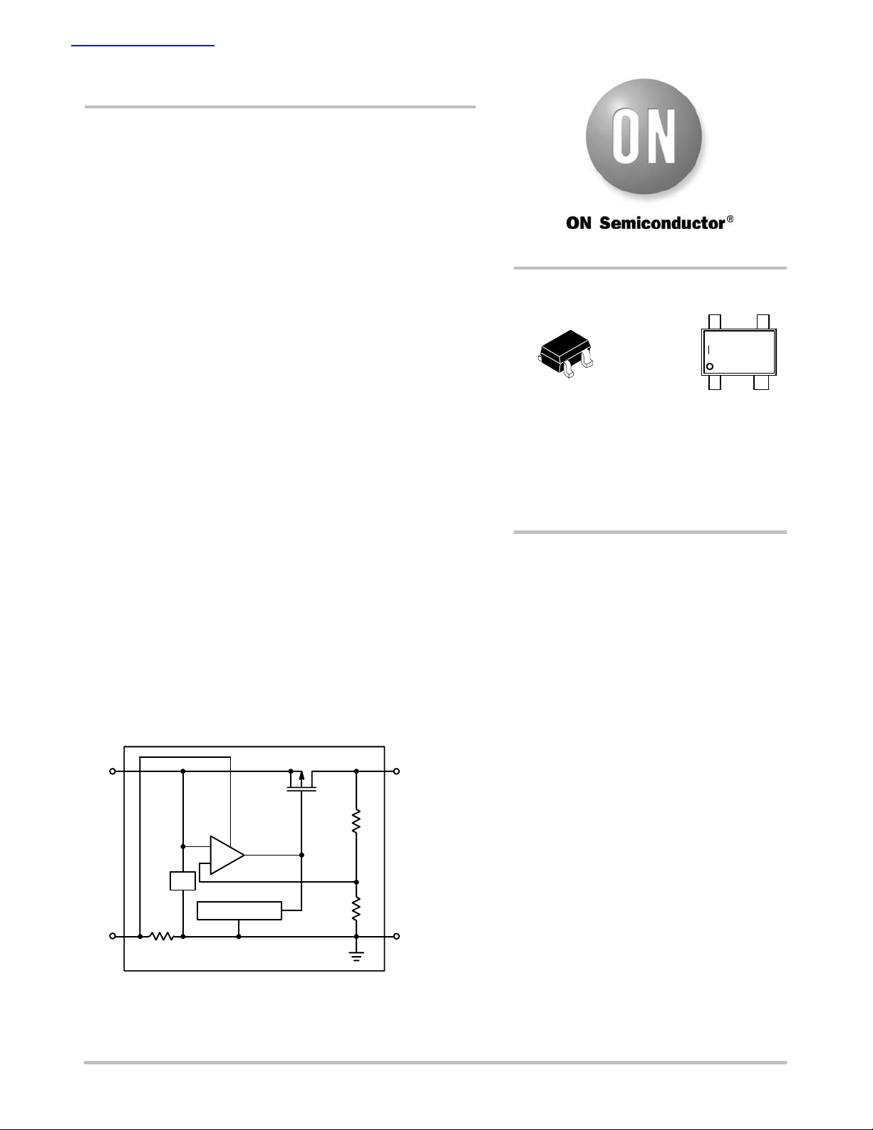
V
in
−
+
V
ref
Current Limit
CE
Figure 1. Simplified Block Diagram
© Semiconductor Components Industries, LLC, 2005
August, 2005 − Rev. 2
V
out
GND
1 Publication Order Number:
NCP580/D
NCP580
PIN FUNCTION DESCRIPTION
Pin Symbol Description
1
V
out
2 GND Power supply ground.
3 CE Chip enable pin.
4 V
in
MAXIMUM RATINGS
Input Voltage V
Input Voltage (CE or CE Pin) V
Output Voltage V
Output Current I
Power Dissipation P
Operating Junction Temperature Range T
Storage Temperature Range T
Maximum ratings are those values beyond which device damage can occur. Maximum ratings applied to the device are individual stress limit values
(not normal operating conditions) and are not valid simultaneously. If these limits are exceeded, device functional operation is not implied, damage
may occur and reliability may be affected.
Regulated output voltage.
Power supply input voltage.
Rating Symbol Value Unit
in
CE
out
out
D
J
stg
6.5 V
−0.3 to Vin +0.3 V
−0.3 to Vin +0.3 V
140 mA
150 mW
−40 to +85 °C
−55 to +150 °C
ELECTRICAL CHARACTERISTICS (V
= V
+ 1.0 V , T
in
out
= 25°C, unless otherwise noted.)
A
Characteristic Symbol Min Typ Max Unit
Input Voltage V
Output Voltage (I
Line Regulation (I
(V
+ 0.5 V v Vin v 6.0 V)
out
(V
= 1.5 V , 2.2 V v Vin v 6.0 V)
out
Load Regulation (I
Dropout Voltage (I
V
= 1.5 V
out
V
= 1.8 V
out
V
= 2.5 V
out
2.8 V v V
Quiescent Current (I
= 1.0 mA to 30 mA)
out
= 30 mA)
out
= 1.0 mA to 120 mA)
out
= 120 mA)
out
v 3.3 V
out
= 0 mA)
out
Output Current I
Shutdown Current (Vin = VCE)
Output Short Circuit Current (V
Ripple Rejection (I
= 30 mA)
out
out
= 0)
f = 1.0 kHz
(V
= 1.5 V , Vin – V
out
(V
w 2.5 V , Vin – V
out
= 1.2 V)
out
= 1.0 V)
out
Enable Input Threshold Voltage
High
Low
Output Noise Voltage (Bandwidth = 10 Hz to 100 kHz) V
Output Voltage Temperature Coefficient
(I
= 30 mA, −40°C v TA v 85°C)
out
DV
2.2 − 6.0 V
V
out
0.985
X
− V
out
1.015
X
− 0.02 0.10 %/V
− 12 40 mV
−
−
−
−
0.36
0.28
0.24
0.18
0.70
0.40
0.35
0.28
V
Reg
Reg
V
in
out
line
load
DO
Iq − 90 160 mA
out
I
SD
I
lim
120 − − mA
0.1 1.0 mA
− 40 − mA
RR
−
−
Vth
enh
Vth
enl
n
/DT − "100 − ppm/°C
out
1.5
0
− 30 − mVrms
75
70
−
−
−
−
V
0.3
in
V
V
dB
V
http://onsemi.com
2
NCP580
.0
3.0
0
1.6
OUTPUT VOLTAGE V
(V)
TYPICAL CHARACTERISTICS
1.4
1.2
out
Vin = 3.5 V
1.0
0.8
0.6
1.8 V
2.5 V
2.0 V
(V)
out
2.5
Vin = 4.8 V
2.0
1.5
1.0
0.4
OUTPUT VOLTAGE V
0.2
0
0 100 150 250
OUTPUT CURRENT I
20050 50 150
(mA)
out
V
= 1.5 V
out
300
0.5
0
0 100 200 250
OUTPUT CURRENT I
Figure 2. Output Voltage vs. Output Current Figure 3. Output Voltage vs. Output Current
1.6
1.5
(V)
out
1.4
1.3
1.2
OUTPUT VOLTAGE V
1.1
I
= 1.0 mA
out
I
= 30 mA
out
I
= 50 mA
out
1.0
1.0 2.0 3.0 4.0
INPUT VOLTAGE Vin (V)
Figure 4. Output Voltage vs. Input Voltage
V
out
5.0
= 1.5 V
6.0
2.9
2.8
(V)
2.7
out
2.6
I
= 1.0 mA
2.5
2.4
2.3
2.2
OUTPUT VOLTAGE V
out
I
= 30 mA
out
I
= 50 mA
out
2.1
2.0
1.0 3.0 4.0 5.0
2.0
INPUT VOLTAGE Vin (V)
Figure 5. Output Voltage vs. Input Voltage
3.8 V
out
(mA)
V
V
3.1 V
out
= 2.8 V
out
3.3 V
= 2.8 V
30
6
100
90
(mA)
80
q
70
60
50
40
30
20
QUIESCENT CURRENT, I
10
0
0
1.0 2.0 3.0 4.0
INPUT VOL TAGE Vin (V)
Figure 6. Quiescent Current vs. Input Voltage
V
= 1.5 V
out
5.0 6.0
http://onsemi.com
100
90
80
(mA)
q
70
60
50
40
30
20
QUIESCENT CURRENT, I
10
0
0
1.0 2.0 3.0 4.0
V
= 2.8 V
out
5.0 6.0
INPUT VOL TAGE Vin (V)
Figure 7. Quiescent Current vs. Input Voltage
3
OUTPUT VOLTAGE, V
(V)
0
2.86
0
QUIESCENT CURRENT, I
(
A)
t
0
out
1.54
1.53
1.52
1.51
NCP580
TYPICAL CHARACTERISTICS
Vin = 2.5 V
I
= 30 mA
out
(V)
out
2.84
2.82
Vin = 3.8 V
I
= 30 mA
out
m
q
1.50
1.49
1.48
1.47
1.46
120
110
100
90
80
70
60
−50
−50
V
= 1.5 V
out
−25 0 25 50
75
TEMPERATURE (°C)
Figure 8. Output Voltage vs. Temperature
V
= 1.5 V
out
Vin = 2.5 V
0 50 100
100
2.80
2.78
OUTPUT VOLTAGE, V
2.76
2.74
−50
120
110
(mA)
q
100
90
80
70
QUIESCENT CURRENT, I
60
−50
V
= 2.8 V
out
−25 0 25 50
75
TEMPERATURE (°C)
Figure 9. Output Voltage vs. Temperature
V
= 2.8 V
out
Vin = 3.8 V
05010
10
TEMPERATURE (°C)
Figure 10. Quiescent Current vs. Temperature
1.2
V
= 1.5 V
out
(V)
1.0
DO
Figure 11. Quiescent Current vs. Temperature
0.25
(V)
0.20
DO
0.8
0.15
TEMPERATURE (°C)
85°C
25°C
0.6
0.4
0.2
DROPOUT VOLTAGE, V
25°C
0.0
0
20 40 60 80
OUTPUT CURRENT I
out
(mA)
Figure 12. Dropout Voltage vs. Output Current
85°C
−40°C
100
120
http://onsemi.com
0.10
0.05
DROPOUT VOLTAGE, V
0.00
−40°C
V
out
0
20 40 60 80
OUTPUT CURRENT I
out
(mA)
Figure 13. Dropout Voltage vs. Output Curren
= 2.8 V
100
12
4

NCP580
TYPICAL CHARACTERISTICS
90
80
70
60
I
= 30 mA
out
I
= 1.0 mA
out
I
= 50 mA
out
50
40
30
20
Vin = 2.5 Vdc + 0.5 Vp−p
RIPPLE REJECTION, RR (dB)
10
C
= Ceramic 2.2 mF
out
0
0.1
1
FREQUENCY, f (kHz)
Figure 14. Ripple Rejection vs. Frequency Figure 15. Ripple Rejection vs. Frequency
10
V
= 1.5 V
out
100
90
I
= 1.0 mA
out
80
70
I
= 30 mA
60
out
I
out
= 50 mA
50
40
30
20
Vin = 3.8 Vdc + 0.5 Vp−p
RIPPLE REJECTION, RR (dB)
10
C
= Ceramic 2.2 mF
out
0
0.1
1
FREQUENCY, f (kHz)
10
V
= 2.8 V
out
100
http://onsemi.com
5

2.83
NCP580
TYPICAL CHARACTERISTICS
= 1.0 mF
C
out
6
2.82
(V)
out
2.81
2.80
2.79
OUTPUT VOLTAGE, V
2.78
2.77
2.83
2.82
(V)
out
2.81
2.80
2.79
OUTPUT VOLTAGE, V
2.78
10 50
0
20 6030 7040 80 90
Input Voltage
Output Voltage
TIME, t (ms)
C
= 2.2 mF
out
Input Voltage
Output Voltage
100
5
4
3
2
1
0
6
5
4
3
2
1
(V)
in
INPUT VOLTAGE, V
(V)
in
INPUT VOLTAGE, V
2.77
2.83
2.82
(V)
out
2.81
2.80
2.79
OUTPUT VOLTAGE, V
2.78
2.77
10 50
0
0
20 6030 7040 80 90
10 50
20 6030 7040 80 90
Figure 16. Input Transient Response
= 3.8 V to 4.8 V, I
(V
in
TIME, t (ms)
C
= 2.2 mF
out
Input Voltage
Output Voltage
TIME, t (ms)
= 30 mA, tr = tf = 5.0 ms, V
out
= 2.8 V)
out
100
100
0
6
5
4
3
2
1
0
(V)
in
INPUT VOLTAGE, V
http://onsemi.com
6

3.00
C
= 1.0 mF
NCP580
TYPICAL CHARACTERISTICS
out
150
2.95
(V)
out
2.90
2.85
2.80
2.75
OUTPUT VOLTAGE, V
2.70
3.00
2.95
(V)
out
2.90
2.85
2.80
16 24
14
18 2620 2822 30 32
Output Current
Output Voltage
TIME, t (ms)
C
= 2.2 mF
out
Output Current
Output Voltage
34
100
50
0
150
100
50
0
(mA)
out
OUTPUT CURRENT, I
(mA)
out
2.75
OUTPUT VOLTAGE, V
2.70
3.00
2.95
(V)
out
2.90
2.85
2.80
2.75
OUTPUT VOLTAGE, V
2.70
= 3.8 V, I
(V
in
16 24
14
14
18 2620 2822 30 32
16 24
18 2620 2822 30 32
Figure 17. Load Transient Response
= 50 mA to 100 mA, tr = tf = 5.0 ms, Cin = 1.0 mF, V
out
TIME, t (ms)
C
= 4.7 mF
out
Output Current
Output Voltage
TIME, t (ms)
= 2.8 V)
out
34
34
150
100
50
0
OUTPUT CURRENT, I
(mA)
out
OUTPUT CURRENT, I
http://onsemi.com
7

NCP580
APPLICATION INFORMATION
Input Decoupling
A 1.0 mF ceramic capacitor is the recommended value to
be connected between Vin and GND. For PCB layout
considerations, the traces of Vin and GND should be
sufficiently wide in order to minimize noise and prevent
unstable operation.
Output Decoupling
It is best to use a 2.2 mF or higher capacitor value on the
V
pin. For better performance, select a capacitor with
out
low Equivalent Series Resistance (ESR). For PCB layout
considerations, place the output capacitor close to the
output pin and keep the leads short as possible.
ORDERING INFORMATION
Nominal
Device Output Type / Features
NCP580SQ15T1G Active High 1.5 AF SC−82AB
NCP580SQ18T1G Active High 1.8 AK SC−82AB
NCP580SQ25T1G Active High 2.5 BF SC−82AB
NCP580SQ28T1G Active High 2.8 BJ SC−82AB
NCP580SQ30T1G Active High 3.0 CA SC−82AB
NCP580SQ33T1G Active High 3.3 CD SC−82AB
†For information on tape and reel specifications, including part orientation and tape sizes, please refer to our Tape and Reel Packaging Specification
Brochure, BRD8011/D.
Output Voltage
Marking Package Shipping†
3000 Tape & Reel
(Pb−Free)
3000 Tape & Reel
(Pb−Free)
3000 Tape & Reel
(Pb−Free)
3000 Tape & Reel
(Pb−Free)
3000 Tape & Reel
(Pb−Free)
3000 Tape & Reel
(Pb−Free)
http://onsemi.com
8

D3 PL
S
A
G
4
3
12
NCP580
PACKAGE DIMENSIONS
SC−82AB
SQ SUFFIX
CASE 419C−02
ISSUE D
NOTES:
1. DIMENSIONING AND TOLERANCING PER
ANSI Y14.5M, 1982.
2. CONTROLLING DIMENSION: MILLIMETER.
3. 419C−01 OBSOLETE. NEW STANDARD IS
419C−02.
C
N
B
F
L
K
H
J
0.05 (0.002)
4. DIMENSIONS A AND B DO NOT INCLUDE
MOLD FLASH, PROTRUSIONS, OR GATE
BURRS.
DIM MIN MAX MIN MAX
A 1.8 2.2 0.071 0.087
B 1.15 1.35 0.045 0.053
C 0.8 1.1 0.031 0.043
D 0.2 0.4 0.008 0.016
F 0.3 0.5 0.012 0.020
G 1.1 1.5 0.043 0.059
H 0.0 0.1 0.000 0.004
J 0.10 0.26 0.004 0.010
K 0.1 −−− 0.004 −−−
L 0.05 BSC 0.002 BSC
N 0.2 REF 0.008 REF
S 1.8 2.4 0.07 0.09
INCHESMILLIMETERS
SOLDERING FOOTPRINT*
1.30
0.512
0.90
0.035
*For additional information on our Pb−Free strategy and soldering
details, please download the ON Semiconductor Soldering and
Mounting Techniques Reference Manual, SOLDERRM/D.
0.70
0.028
0.65
0.026
0.95
0.037
SCALE 10:1
1.90
0.075
mm
ǒ
inches
Ǔ
http://onsemi.com
9

NCP580
ON Semiconductor and are registered trademarks of Semiconductor Components Industries, LLC (SCILLC). SCILLC reserves the right to make changes without further notice
to any products herein. SCILLC makes no warranty, representation or guarantee regarding the suitability of its products for any particular purpose, nor does SCILLC assume any
liability arising out of the application or use of any product or circuit, and specifically disclaims any and all liability, including without limitation special, consequential or incidental
damages. “Typical” parameters which may be provided in SCILLC data sheets and/or specifications can and do vary in different applications and actual performance may vary over
time. All operating parameters, including “Typicals” must be validated for each customer application by customer’s technical experts. SCILLC does not convey any license under
its patent rights nor the rights of others. SCILLC products are not designed, intended, or authorized for use as components in systems intended for surgical implant into the body,
or other applications intended to support or sustain life, or for any other application in which the failure of the SCILLC product could create a situation where personal injury or death
may occur. Should Buyer purchase or use SCILLC products for any such unintended or unauthorized application, Buyer shall indemnify and hold SCILLC and its officers, employees,
subsidiaries, affiliates, and distributors harmless against all claims, costs, damages, and expenses, and reasonable attorney fees arising out of, directly or indirectly, any claim of
personal injury or death associated with such unintended or unauthorized use, even if such claim alleges that SCILLC was negligent regarding the design or manufacture of the part.
SCILLC is an Equal Opportunity/Affirmative Action Employer. This literature is subject to all applicable copyright laws and is not for resale in any manner.
PUBLICATION ORDERING INFORMATION
LITERATURE FULFILLMENT:
Literature Distribution Center for ON Semiconductor
P.O. Box 61312, Phoenix, Arizona 85082−1312 USA
Phone: 480−829−7710 or 800−344−3860 Toll Free USA/Canada
Fax: 480−829−7709 or 800−344−3867 Toll Free USA/Canada
Email: orderlit@onsemi.com
N. American Technical Support: 800−282−9855 Toll Free
USA/Canada
Japan: ON Semiconductor, Japan Customer Focus Center
2−9−1 Kamimeguro, Meguro−ku, Tokyo, Japan 153−0051
Phone: 81−3−5773−3850
http://onsemi.com
ON Semiconductor Website: http://onsemi.com
Order Literature: http://www.onsemi.com/litorder
For additional information, please contact your
local Sales Representative.
NCP580/D
10

Copyright © Each Manufacturing Company.
All Datasheets cannot be modified without permission.
This datasheet has been download from :
www.AllDataSheet.com
100% Free DataSheet Search Site.
Free Download.
No Register.
Fast Search System.
www.AllDataSheet.com
 Loading...