

NCP5010
e
500 mW Boost Converter for
White LEDs
The NCP5010 is a fixed frequency PWM boost converter with
integrated rectification optimized for constant current applications
such as driving white LEDs. This device features small size, minimal
external components and high−efficiency for use in portable
applications and is capable of providing up to 500 mW output power
to 2−5 series connected white LEDs. A single resistor sets the LED
current and the CTRL pin can be pulse width modulated (PWM) to
reduce the LED Current.
The device includes True−Cutoff circuitry to disconnect the load
from the battery when the device is put into standby mode. To protect
the device, an output overvoltage protection, and short circuit
protection have been incorporated. The NCP5010 is housed in a low
profile, space efficient 1.7 x 1.7 mm Flip−Chip package. The device
has been optimized for use with small inductors and ceramic
capacitors.
Features
• 2.7 to 5.5 V Input Voltage Range
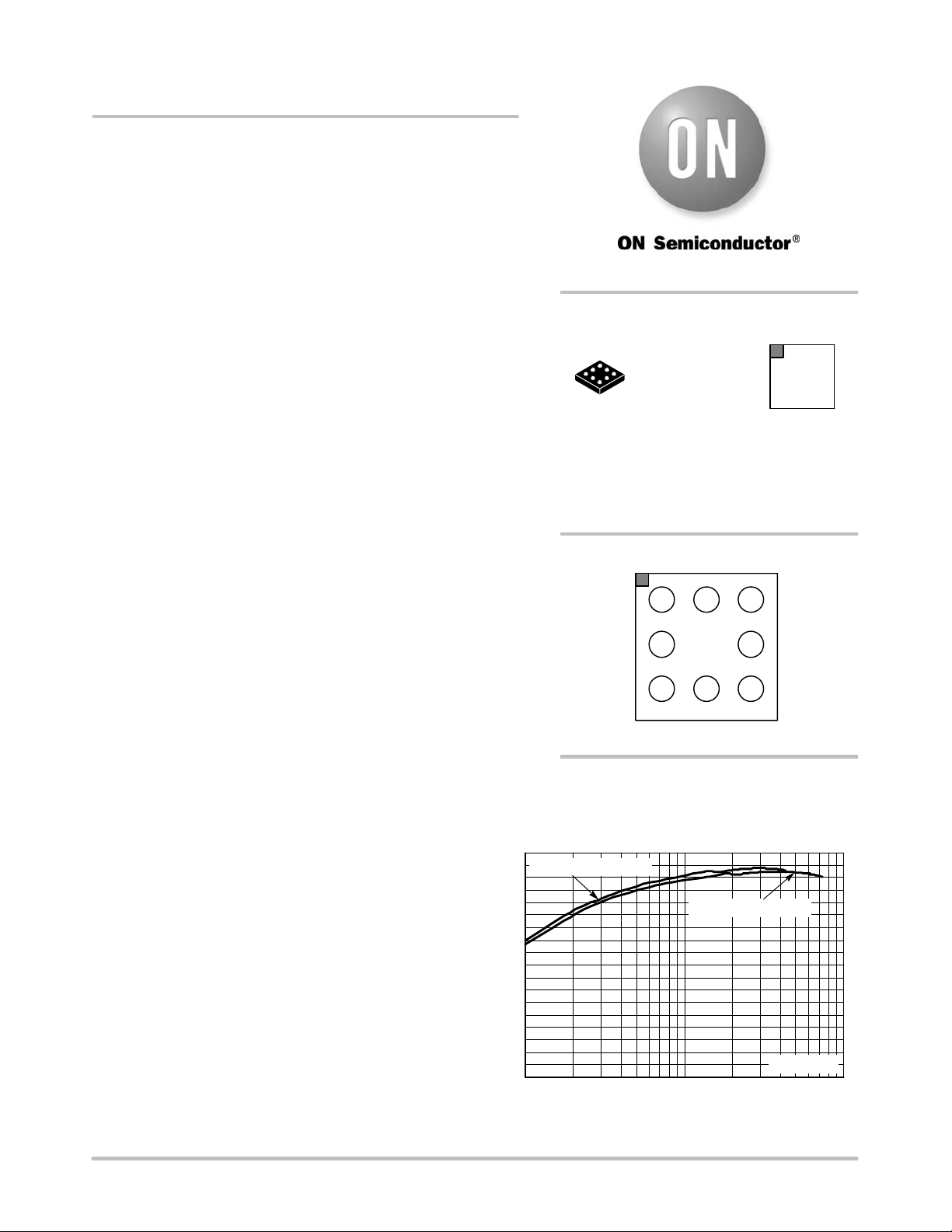
• Efficiency: 84% for 5 LED (V
4.2 V V
IN
• Low Noise 1 MHz PWM DC−DC Converter
• Open LED Protection and Short Circuit Protection
• Serial LEDs Architecture for Uniform Current Matching
• 1 mA Shutdown Current Facility with True−Cutoff
• Very Small 8−Pin Flip−Chip 1.7 x 1.7 mm Package
• This is a Pb−Free Device
T ypical Applications
• White LED Backlighting for Small Color LCD Displays
• Cellular Phones
• Digital Cameras
• MP3 Players
• High Efficiency Step−up Converter
= 3.5 V by LED) at 30 mA and
F
90
80
70
60
50
40
30
EFFICIENCY (%)
20
10
http://onsemi.com
MARKING
DIAGRAM
A1
8−Pin Flip−Chip
FC SUFFIX
1
See detailed ordering and shipping information in the packag
dimensions section on page 16 of this data sheet.
V
= 5 LED (18 V)
OUT
0
1 10 100
Figure 1. Efficiency vs. Output Current
CASE 499AJ
DAX = Specific Device Code
G = Pb−Free Package
A = Assembly Location
Y = Year
WW = Work Week
PIN CONNECTIONS
A1
A2 A3
AGND
CTRL NC
B1 B3
V
IN
C1 C2 C3
V
ORDERING INFORMATION
OUT
I
OUT
SW PGND
Top View
V
= 3 LED (11 V)
OUT
(mA)
DAXG
AYWW
FB
VIN = 4.2 V
© Semiconductor Components Industries, LLC, 2007
March, 2007 − Rev. 2
1 Publication Order Number:
NCP5010/D
V
bat
2.7 to 5.5 V
NCP5010
C
in
4.7 mF 0603
L1
22 mH
LED
X5R 6.3V
C2
IN
SW
ENABLE
A2
CTRL
A3
NC
NCP5010
V
AGND
A1 B1
V
PGND
C3
OUT
B3
FB
C1
C
out
1 mF 0805
X5R 25V
R
24
LED
fb
2 to 5 LEDs
Figure 2. Typical Application Circuit
PIN FUNCTION DESCRIPTION
PIN PIN NAME TYPE DESCRIPTION
A1 AGND POWER System ground for the analog circuitry . A high quality ground must be provided to avoid spikes and/
B1 V
C1 V
IN
OUT
POWER Power Supply Input. A ceramic capacitor with a minimum value of 1 mF/6.3 V (X5R or X7R) must be
POWER DC−DC converter output. This pin should be directly connected to the load and a low ESR
A2 CTRL INPUT An Active High logic level on this pin enables the device. A built−in pulldown resistor disables the
C2 SW POWER Power switch connection for inductor. T ypical application will use a coil from 10 mH to 22 mH and
A3 NC N/A Not Connected
B3 FB INPUT Feedback voltage input used to close the loop by means of a sense resistor connected between the
C3 PGND POWER Power ground. A high quality ground must be used to avoid spikes and/or uncontrolled operation.
or uncontrolled operations. This pin is to be connected to the PGND pin.
connected to this pin. This capacitor should be placed as close as possible to this pin. In addition,
one end of the external inductor is to be connected at this point.
(<30 mW) 1 mF (min) 25 V bypass capacitor. This capacitor is required to smooth the current flowing
into the load, thus limiting the noise created by the fast transients present in this circuit. Since this is
a current regulated output, this pin has over voltage protection to protect from open load conditions.
Care must be taken to avoid EMI through the PCB copper tracks connected to this pin.
device if the pin is left open. This pin can also be used to control the average current into the load
by applying a low frequency PWM signal. If a PWM signal is applied, the frequency should be high
enough to avoid optical flicker but be no greater than 1 kHz.
must be able to handle at least 350 mA. If the desired output power is above 300 mW, the inductor
should have a DCR < 1.4 W.
primary LED branch and the ground. The output current tolerance is depends upon the accuracy of
this resistor and a ±5% or better accuracy metal film resistor is recommended. An analog dimming
signal can be applied to this point to reduce the output current. Please refer to the application
section for additional details.
Care must be taken to avoid high−density current flow in a limited PCB copper track. This pin is to
be connected to the AGND pin.
http://onsemi.com
2

NCP5010
MAXIMUM RATINGS
Rating Symbol Value Unit
Power Supply Voltage (Note 2) V
Over Voltage Protection V
IN
OUT
Human Body Model (HBM) ESD Rating (Note 3) ESD HBM 2000 V
Machine Model (MM) ESD Rating (Note 3) ESD MM 200 V
Digital Input Voltage
CTRL −0.3 < VIN < V
Digital Input Current
Power Dissipation @ TA = +85 °C P
Thermal Resistance Junction−to−Air
D
R
q
JA
8−Pin Flip−Chip Package
Operating Ambient Temperature Range T
Operating Junction Temperature Range T
Storage Temperature Range T
A
J
stg
Stresses exceeding Maximum Ratings may damage the device. Maximum Ratings are stress ratings only. Functional operation above the
Recommended Operating Conditions is not implied. Extended exposure to stresses above the Recommended Operating Conditions may affect
device reliability.
1. Maximum electrical ratings are defined as those values beyond which damage to the device may occur at TA = 25°C.
2. According to JEDEC standard JESD22−A108B.
3. This device series contains ESD protection and passes the following tests:
Human Body Model (HBM) ±2.0 kV per JEDEC standard: JESD22−A114 for all pins.
Machine Model (MM) ±200 V per JEDEC standard: JESD22−A115 for all pins.
4. Latchup Current Maximum Rating: ±100 mA per JEDEC standard: JESD78.
5. Moisture Sensitivity Level (MSL): 1 per IPC/JEDEC standard: J−STD−020A.
6. For the 8−Pin Flip−Chip CSP Package, the R
50 mm total area and also 135°C/W with 500 mm. All the bumps have the same thermal resistance and need to be connected thereby optimizing
is highly dependent on the PCB Heatsink area. For example R
q
JA
the power dissipation.
7.0 V
24 V
+0.3
bat
1.0
mA
150 mW
°C/W
(Note 6)
−40 to +85 °C
−40 to +125 °C
−65 to +150 °C
can be to 195°C/W with
q
JA
V
http://onsemi.com
3

NCP5010
ELECTRICAL CHARACTERISTICS (Limits apply for T
between −40°C to +85°C and VIN = 3.6 V , unless otherwise noted)
A
Pin Symbol Rating Min Typ Max Unit
B1 V
C2 I
IN
PEAK_MAX
NMOS R
F
OSC
M
DUTY
E
FF
C1 OVP
C1 OVP
C1 P
C1 I
B3 F
C1 F
OUT
OUT
BV
BVLR
DS(on)
ON
H
Supply Voltage 2.7 5.5 V
Switch Current Limit 280 420 560 mA
Internal Switch On Resistor 0.6 1.0 W
PWM Oscillator Frequency 0.8 1.0 1.2 MHz
Maximum Duty Cycle 91 95 %
Efficiency (Note 7) 84 %
Overvoltage Clamp Voltage 20 22 V
Overvoltage Clamp Hysteresis 1.0 V
Output power (Note 8)
VIN = 3.1 V
VIN < 3.1 V
Minimum Output Current Controlled No Skip Mode
500
300
1.0 mA
(Note 9)
Feedback Voltage Threshold in Steady State
Overtemperature range
At 25°C
475
490
500
500
525
510
Feedback Voltage Line Regulation (Notes 9 and 10)
From DC to 100 Hz 0.2 0.5
B1 U
B1 U
C1 I
B1 S
VLO
VLOH
OUTSC
CPT
B1C2ISTDB Stand by Current, I
I
Q
A2 V
A2 V
A2 R
IL
IH
CTRL
7. Efficiency is defined by 100 * (P
VIN = 4.2 V with L= Coilcraft DT1608C−223
I
= 30 mA, Load = 5 LEDs (VF = 3.5 V per LED) bypassed by 1 mF X5R
OUT
VIN Undervoltage Lockout measured at 25°C
Threshold to Enable the Converter
Threshold to Disable the Converter
2.2
2.0
2.4
2.2
2.6
2.4
Undervoltage Lockout Hysteresis 200 mV
Short Circuit Output Current 20 mA
Short Circuit Protection Threshold
Detected
Released
V
bat
= 4.2 V
= 0 mA, CTRL = Low
OUT
35
47
50
67
65
87
2.0 mA
Quiescent Current
Device Not Switching (BF = VIN)
Device Switching (RFB disconnected)
0.4
1.0
Voltage Input Logic Low 0.3 V
Voltage Input Logic High 1.2 V
CTRL Pin Pulldown Resistance 175 370 kW
/ Pin) at 25°C
out
8. Guaranteed by design and characterized with L = 22 mH, DCR = 0.7 W max.
9. Load = 4 LEDs (VF = 3.5 V by LED), C
10.VIN = 3.6 V , Ripple = 0.2 V P−P, I
OUT
= 1 mF X5R, L= Coilcraft DT1608C−223.
OUT
= 15 mA.
mW
mV
%/V
V
% of V
mA
IN
http://onsemi.com
4
NCP5010
)
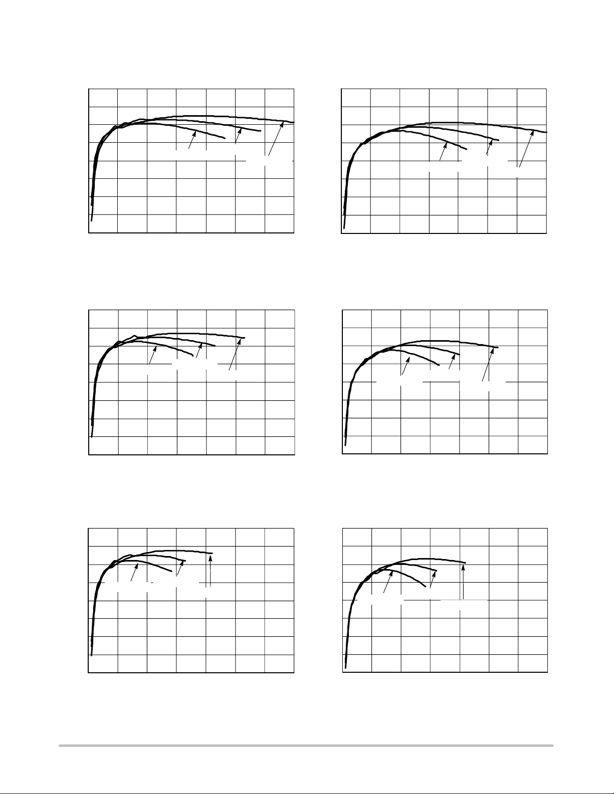
TYPICAL OPERATING CHARACTERISTICS
0
0
0
Condition: Efficiency = 100 x (Number of LED stacked x V
90
80
70
EFFICIENCY (%)
60
50
010203040506070
VIN = 2.7 V
I
OUT
VIN = 3.3 V
VIN = 4.2 V
(mA)
Figure 3. Efficiency vs. Current @ 3 LEDS (10.5 V)
L = Coilcraft DT1608C−223
90
80
x I
LED
90
80
70
EFFICIENCY (%)
60
50
0 1020304050607
)/P
LED
IN
VIN = 2.7 V
I
(mA)
OUT
VIN = 3.3 V
VIN = 4.2 V
Figure 4. Efficiency vs. Current @ 3 LEDS (10.5 V)
L = TDK VLF4012AT−220
90
80
VIN = 2.7 V
70
EFFICIENCY (%)
60
50
0 10203040506070
VIN = 3.3 V
I
(mA)
OUT
VIN = 4.2 V
Figure 5. Efficiency vs. Current @ 4 LEDS (14 V)
L = Coilcraft DT1608C−223
90
80
VIN = 2.7 V
70
EFFICIENCY (%)
60
VIN = 3.3 V
VIN = 4.2 V
70
EFFICIENCY (%)
60
50
0 1020304050607
VIN = 2.7 V
VIN = 3.3 V
I
(mA)
OUT
VIN = 4.2 V
Figure 6. Efficiency vs. Current @ 4 LEDS (14 V)
L = TDK VLF4012AT−220
90
80
70
EFFICIENCY (%)
60
VIN = 2.7 V
VIN = 3.3 V
VIN = 4.2 V
50
0 10203040506070
I
(mA)
OUT
Figure 7. Efficiency vs. Current @ 5 LEDS (17.5 V)
L = Coilcraft DT1608C−223
http://onsemi.com
50
0 1020304050607
I
(mA)
OUT
Figure 8. Efficiency vs. Current @ 5 LEDS (17.5 V
L = TDK VLF4012AT−220
5
NCP5010
0
TYPICAL OPERATING CHARACTERISTICS
.5
00
Condition: Efficiency = 100 x (Number of LED stacked x V
90
I
= 33 mA
OUT
80
I
= 10 mA
70
I
OUT
= 23 mA
OUT
60
50
EFFICIENCY (%)
40
I
OUT
= 1 mA
30
20
2.5 3.0 3.5 4.0 4.5 5.0 5.5
VIN (V)
Figure 9. Efficiency vs. VIN @ 3 LEDS (10.5 V)
L = Coilcraft DT1608C−223
90
80
70
I
OUT
= 28 mA
I
OUT
= 23 mA
I
OUT
= 10 mA
x I
LED
)/P
IN
LED
90
I
= 33 mA
OUT
80
70
I
OUT
= 23 mA
I
OUT
60
50
EFFICIENCY (%)
40
I
OUT
30
20
2.5 3.0 3.5 4.0 4.5 5.0 5
VIN (V)
Figure 10. Efficiency vs. VIN @ 4 LEDS (14 V)
L = Coilcraft DT1608C−223
510
505
VIN = 3.6 V
= 10 mA
= 1 mA
60
I
50
EFFICIENCY (%)
40
OUT
= 1 mA
30
20
2.5 3.0 3.5 4.0 4.5 5.0 5.5
VIN (V)
Figure 11. Efficiency vs. V
@ 5 LEDS (17.5 V)
IN
L = Coilcraft DT1608C−223
1.04
VIN = 3.6 V
1.02
1.00
FREQUENCY (MHz)
0.98
VIN = 2.7 V
VIN = 5.5 V
VIN = 5.5 V
500
VIN = 2.7 V
495
FEEDBACK VOLTAGE (mV)
490
−40 −20 0 20 40 60 80 10
TEMPERATURE (°C)
Figure 12. Feedback Voltage vs. Temperature
900
800
700
(mW)
DS(on)
600
500
NMOS R
400
VIN = 3.6 V
VIN = 2.7 V
VIN = 5.5 V
0.96
−40 −20 0 20 40 60 80 100
300
−40 −20 0 20 40 60 80 1
TEMPERATURE (°C)
Figure 13. Oscillator Frequency vs. Temperature Figure 14. NMOS R
http://onsemi.com
6
TEMPERATURE (°C)
vs. Temperature
DS(on)

NCP5010
TYPICAL OPERATING CHARACTERISTICS
I
(mA)
3
2
OUT
1
0
2.5 3.0 3.5 4.0 4.5 5.0 5.5
3 LEDs
VIN (V)
4 LEDs
5 LEDs
Figure 15. Typical Skip Mode Threshold vs. V
(C
= 1 mF X5R 25 V)
OUT
IN
Figure 16. Typical V
, 500 mV/div, AC 3 V
1 V
OUT
Ripple in OVP Conditions
OUT
, 5 V/div , DC
OUT
Figure 17. Continuous Current Mode (CCM)
1 SW, 5 V/div DC, 4 I
, 50 mA/div , DC, I
SW
OUT
Figure 19. Startup for LED Operating, 4 LEDS
= 22 W, 1 CTRL, 2 V/div DC, 2 FB, 500 mV/div DC,
R
BF
100 mA/div, T = 100 ms/div
4 I
L
= 15 mA
http://onsemi.com
7
Figure 18. Discontinuous Current Mode (DCM)
1 SW, 5 V/div DC, 4 ISW, 50 mA/div , DC, I
OUT
Figure 20. Duty Cycle Control Waveforms
1 CTRL, 2 V/div DC, 2 FB, 500 mV/div DC,
100 mA/div, T = 1 ms/div
4 I
L
= 1 mA

NCP5010
TYPICAL OPERATING CHARACTERISTICS
Figure 21. Typical Ripple for Voltage Operation
1 SW, 10 V/div DC, 2 FB, 500 mV/div DC, 3 V
20 mV/div AC, T = 500 ns/div
OUT
http://onsemi.com
8
NCP5010
V
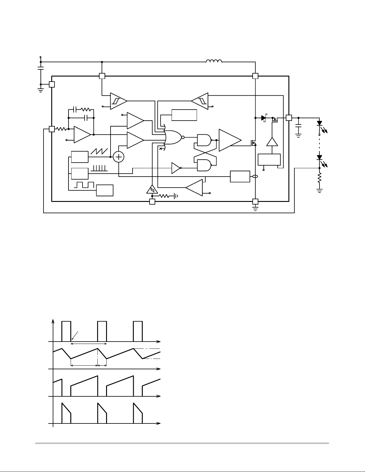
DETAIL OPERATING DESCRIPTION
Bat
2.7 to 5.5 V
C
in
1 mF, 6.3 V X5R 0603
A1
AGND
FB
B3
FB REF
CLOCK
−
ERROR
AMP
+
RAMP
COMP
ONE
SHOT
B1
UVLO REF
M DUTY REF
OSC
1 Mhz
L
IPEAK
COMP
22 mH
+
−
OVP REF
DRIVER
SENSE
+
−
IPEAK MAX
CURRENT
PGND
V
IN
UVLO
COMP
−
+
UVLO
MAX DUTY
CYCLE COMP
−
MAX D
+
−
PWM
COMP
+
CTRL
CTRL
IPEAK MAX
250 k
A2
OVP
COMP
OVP
THERMAL
PROTECTION
RST
SET
SW
C2
NMOS
SHORT
CIRCUIT
PROTECTION
V
C3
SC
IN
DRIVER
V
OUT
C1
X5R 0805
C
out
1 mF
25 V
Up to 22 V
R
FB
Figure 22. Functional Block Diagram
Operation
The NCP5010 DC−DC converter is based on a Current
Mode PWM architecture which regulates the feedback
voltage at 500 mV under normal operating conditions. The
boost converter operates in two separate phases (See
Figure 23). The first one is TON when the inductor is
charged by current from the battery to store up energy,
followed by T
step where the power is transmitted
OFF
through the internal rectifier to the load. The capacitor
C
is used to store energy during the T
OUT
supply current to the load during the TON stage thus
time and to
OFF
constantly powering the load.
Start
SW
IL
Cycle
1 MHz
I
peak
I
T
T
on
off
valley
The internal oscillator provides a 1 MHz clock signal to
trigger the PWM controller on each rising edge (SET signal)
which starts a cycle. During this phase the low side NMOS
switch is turne d on thus increasing the current through the
inductor. The switch current is measured by the SENSE
CURRENT and added to the RAMP COMP signal. Then
PWM COMP compares the output of the adder and the signal
from ERROR AMP. When the comparator threshold is
exceeded, the N M OS s w itch is turn ed off until the ris ing e dg e
of the next clock cycle. In addition, there are six functi ons
which can re set the flip −flop logic to swi tc h off the NMOS.
The MAX DUTY CYCLE COMP moni tors the pulse width
and if it exceeds 95% (nom) of the cycle ti me the sw itch will
be turned off. Thi s lim it s the swit ch from bei ng on for more
than one cycle. Due t o IP EAK COMP, the current through the
inductor is monitored and compared with the I
PEAK_MAX
threshold set at 440 mA (nom). If the current exceeds this
value, the controller is will turn off the NMOS sw itch for the
remainder of t he c ycle. T his is a safety f unction t o p revent a ny
excessive current that could ove rload the induct or and the
power stage. The four other safety circuits are SHORT
I
SW
CIRCUIT PROTECTION, OVP, UVLO, and THERMAL
PROTECTION. Please refer to the detail in following
sections.
The loop stability is compensated by the ERROR AMP
I
out
built in integrator. The gain and the loop bandwidth are
fixed internally and provides a phase margin greater than
45° whatever the current supplied.
Figure 23. Basic DC−DC Operation
http://onsemi.com
9

NCP5010
LED Current Selection
The feedback resistor (RFB) determines the average
maximum current through the LED string. The control loop
regulated the current such that the average voltage at the FB
input is 500 mV (nom). For example, should one need a
20 mA output current in the primary branch, RFB should be
selected according to the following equation:
FB
+
F
I
OUT
R
BV
+
500 mV
20 mA
+ 25 W
In white LED applications it is desirable to operate the
LEDs at a specific operating current as the color will shift
as the bias current is changed. As a result of this effect, it
is recommended to dim the LED string by a pulse width
modulation techniques. A low frequency PWM signal can
be applied to the CTRL input and by varying the duty cycle
the brightness of the LED can be changed. To avoid any
optical flicker, the frequency must be higher than 100 Hz
and preferably less than 1 kHz. Due to the soft−start
function set at 600 ms (nom) with higher frequency the
device remains active but the brightness can decrease.
Nevertheless in this case, a dimming control using a
filtered PWM signal (See Figure 33) can be used. Also for
DC voltage control the same technique is suitable and the
filter is takes away.
Inductor Selection
To choose the inductor there are three dif ferent electrical
parameters that need to be considered, the absolute value
of the inductor, the saturation current and the DCR. In
normal operation, this device is intended to operate in
Continuous Conduction Mode (CCM) so the following
equation below can be used to calculate the peak current:
I
+
(
h
1 * D
OUT
I
PEAK
In the equation above, VIN is the battery voltage, I
VIND
)
)
2LF
is
OUT
the load current, L the inductor value, F the switching
frequency, and the duty cycle D is given by:
V
IN
D +ǒ1 *
V
Ǔ
OUT
h is the global converter efficiency which can vary with
load current (see Figure 3 thru Figure 8). A good
approximation is to use h = 0.8. Figure 24 − Figure 26 are
a graphical representation of the above equations, as a
function of the desired I
, VIN, and number of LEDs in
OUT
series (VF = 3.5 V nominal). The curves are limited to an
I
PEAK_MAX
of 300 mA. It is important to analyze this at
worst case Vf conditions to ensure that the inductor current
rated is high enough such that it not saturate.
The recommended inductor value should range between
10 mH and 22 mH. As can be seen from the curves, as the
inductor size is reduced, the peak current for a given set of
conditions increases along with higher current ripple so it
is not possible to deliver maximum output power at lower
inductor values.
300
L = 10 mH
250
200
(mA)
150
PEAK
I
100
50
10 20 30 40 50 60 70 80
Figure 24. Peak Inductor Currents vs. I
L = 15 mH
L = 22 mH
I
OUT
(mA)
VIN = 3.1 V
V
IN
OUT
@ 3 LEDs, 10.5 V
300
L = 10 mH
250
200
(mA)
150
PEAK
I
L = 15 mH
100
50
10 20 30 40 50 60 70 80
L = 22 mH
I
OUT
(mA)
Figure 25. Peak Inductor Currents vs. I
VIN = 3.1 V
IN
OUT
@ 4 LEDs, 14 V
300
250
200
(mA)
150
PEAK
I
100
50
10 20 30 40 50 60 70 80
L = 10 mH
L = 15 mH
L = 22 mH
I
OUT
(mA)
VIN = 3.1 V
= 4.2 VV
IN
Figure 26. Peak Inductor Currents vs. I
@ 5 LEDs, 17.5 V
= 4.2 V
(mA)
= 4.2 VV
(mA)
OUT
(mA)
http://onsemi.com
10

NCP5010
Finally an acceptable DCR must be selected regarding
losses in the coil and must be lower than 1.4 W to limit
excessive voltage drop. In addition, as DCR is reduced,
overall efficiency will improve. Some recommended
inductors include but are not limited to:
TDK VLF4012AT−220MR51
TDK VLP4612T−220MR34
TDK VLP5610T−220MR45
Coilcraft LPO6610−223M
Coilcraft DO1605T−223MX
Coilcraft DT1608C−223
Capacitor Selection
To minimize the output ripple, a low ESR multi−layer
ceramic capacitor type X5R or equivalent should be
selected. For LED driver applications a 1 mF (min) 25 V is
adequate. The NCP5010 can be operated in a voltage mode
configuration (see Figure 34) for applications such as
OLED power. Under these conditions, C
OUT
can be
increased to 2.2 mF, 25 V or more to reduce the output
ripple.
The input needs to be bypassed by a X5R or an equivalent
low ESR ceramic capacitor near the VIN pin. A 1 mF, 6.3 V
is enough for most applications. However, if the connection
between VIN and the battery is too long then a 4.7 mF or
higher ceramic capacitor may be needed. Some
recommended capacitors include but are not limited to:
TDK C1608X5R1E105MT
TDK C2012X5R1E105MT
TDK C1608X5R0J105MT
TDK C2012X5R1E225MT
Murata GRM185R61A105KE36D
Murata GRM188R60J475KE19D
Murata GRM216R61E105KA12D
Short−Circuit Protection
If V
is falls below 50% of VIN then a short−circuit
OUT
condition is detected. When this event is detected, the
PWM circuitry is disabled and the NMOS power switch is
not turned on. Power will be supplied to the load through
the inductor, rectifier and high side switch. Once V
OUT
reaches 66% of VIN, then the PWM circuitry is enabled. In
normal conditions when the device is enabled by an active
high signal on CTRL, the short circuit condition continues
until the output capacitor is charged by the limited current
up to 66% of VIN.
V
OUT
2/3 V
IN
1/2 V
IN
Normal
Running
Figure 27. Example of the V
When Short−Circuit Arises
Overvoltage Protection (OVP)
Short−Circuit Condition
SC
Current limited at 20mA
Occurs
Converter in Standby
End of Short−Circuit
Detected Converter
Starts Again
Voltage Behavior
OUT
If there is an open load condition such as a loose
connection to the White LED string, the converter will
provide current to the C
capacitor and the voltage at the
out
output will rise rapidly. This could cause damage to the part
if there was not some external clamping Zener clamping
circuit. To eliminate the need for these external
components, the NCP5010 incorporates an OVP circuit
which monitors the output voltage with a resistive divider
network and a comparator and voltage reference. If the
output reaches 22 V (nominal), the OVP circuit will detect
a fault and inhibit PWM operation. This comparator has
1 V of hysteresis so when the load is reconnected and the
voltage drops below 21 V, the PWM operation will resume
automatically. The 22 V OVP threshold allows the use of
25 V ceramic capacitors for the output filter capacitor.
Undervoltage Lock Out (UVLO)
To ensure proper operation under all conditions, the
device has a built−in undervoltage lock out (UVLO)
circuit. During power−up, the device will remain disabled
until the input voltage exceeds 2.4 V nominal. This circuit
has 200 mV of hysteresis to provide noise immunity to
transient conditions.
T
http://onsemi.com
11

NCP5010
Layout Recommendations
As with all switching DC/DC converter, care must be
observed to the PCB board layout and component
placement. To prevent electromagnetic interference (EMI)
problems and reduce voltage ripple of the device any
copper trace which see high frequency switching path
should be optimized. So the input and output bypass
ceramic capacitor, CIN and C
be placed as close as possible the NCP5010 and connected
directly between pins and ground plane. In additional, the
track connection between the inductor and the switching
input, SW pin must be minimized to reduce EMI radiation.
Finally it is always good practice to keep way sensitive
tracks such as feedback connection from switched signal
like SW or VOUT connections. Figure 28 shown an
example of optimized PCB layout.
as depicted Figure 2 must
OUT
Figure 28. Recommended PCB Layout
http://onsemi.com
12

NCP5010
TYPICAL APPLICATION CIRCUITS
Basic Feedback
Figure 29 is a basic application where a regulated courant
is drive in a string of LEDs. A 20.8 mA current is fixed by
R1 and LEDs are dim with PWM apply on CTRL pin.
V
Bat
2.7 to 5.5 V
L1
B1
IN
V
AGND
A1
C2
SW
V
OUT
PGND
C3
22 mH
C1
FB
B3
C
in
4.7 mF 0603
X5R 6.3 V
PWM
A2
NCP5010
CTRL
LED
2 to 5 LEDs
LED
R1
24
C2
1 mF 0805
X5R 25 V
L1: TDK VLF4012A T−220MR51
C1: TDK C1608X5R0J475MT
C2: TDK C2012X5R1E105MT
Figure 29. Typical Semi−Pulsed Mode of Operation
Different Supply
The NCP5010 can operate from two different supply:
One end of the inductor (V
) can be directly connected
BAT
to a battery like 4 cell alkaline or 2 cell Li−Ion. And VIN pin
V
Bat
V
in
C
4.7 mF 0603
X5R 6.3 V
ENABLE
2.7 to 5.5 V
in
A2
CTRL
NCP5010
Figure 30. Operate from Different Supply
B1
IN
V
AGND
A1
C2
SW
V
OUT
PGND
C3
L1
22 mH
C1
FB
B3
need a power delivered for example from an LDO. Care
must be observed to have always V
minimum output voltage range will be V
LED
LED
R1
24
C2
1 mF 0805
X5R 25 V
2 to 5 LEDs
L1: TDK VLF4012A T−220MR51
C1: TDK C1608X5R0J475MT
C2: TDK C2012X5R1E105MT
above VIN and
BAT
voltage.
BAT
http://onsemi.com
13

NCP5010
Multiple LEDs String
Since the output voltage in limited at 22 V (nom.), one
can arrange the LEDs in 2 or more string. Figure 31 shows
V
Bat
2.7 to 5.5 V
L1
C1
4.7 mF 0603
X5R 6.3 V
ENABLE
X5R 6.3 V
A2
CTRL
NCP5010
ENABLE SECONDARY BRANCH
Figure 31. Multiple LED String Application
22 mH
C2
IN
SW
V
AGND
A1 B1
C3
PRIMARY BRANCH
V
OUT
PGND
B3
C1
FB
two LEDs branches where the constant current is regulated
in primary branch and the secondary branch is selected by
Q1. The number of LED in each string have to be the same.
LED
2 to 5 LEDs
LED
R1
24
LED
LED
R2
24
Q1
N
C2
1 mF 0805
X5R 25 V
L1: TDK VLF4012A T−220MR51
C1: TDK C1608X5R0J475MT
C2: TDK C2012X5R1E105MT
Matched LEDs Branches
Should one need to control precisely the current in two
LEDs branches the schematic Figure 32 can be used. An
dual NPN BC847BD is used to form a current mirror Q1
V
Bat
2.7 to 5.5 V
L1
C1
4.7 mF 0603
X5R 6.3 V
ENABLE
X5R 6.3 V
A2
NCP5010
CTRL
IN
V
AGND
A1 B1
C2
SW
V
OUT
PGND
C3
22 mH
FB
B3
C1
I1 I2
R1
24
like this the current in the secondary branch I2 equal the
current in primary branch I1. Thank to this current mirror
the number of LEDs in secondary branch could be lower or
equal than primary one.
LED
2 to 5 LEDs
LED
LED
LED
Q1
R2
24
C2
1 mF 0805
X5R 25 V
NPN Duals
Q1: ON SEMICONDUCTOR BC847BDW1T1
L1: TDK VLF4012A T−220MR51
C1: TDK C1608X5R0J475MT
C2: TDK C2012X5R1E105MT
Figure 32. Matched 2 Branches of LEDs
http://onsemi.com
14
NCP5010
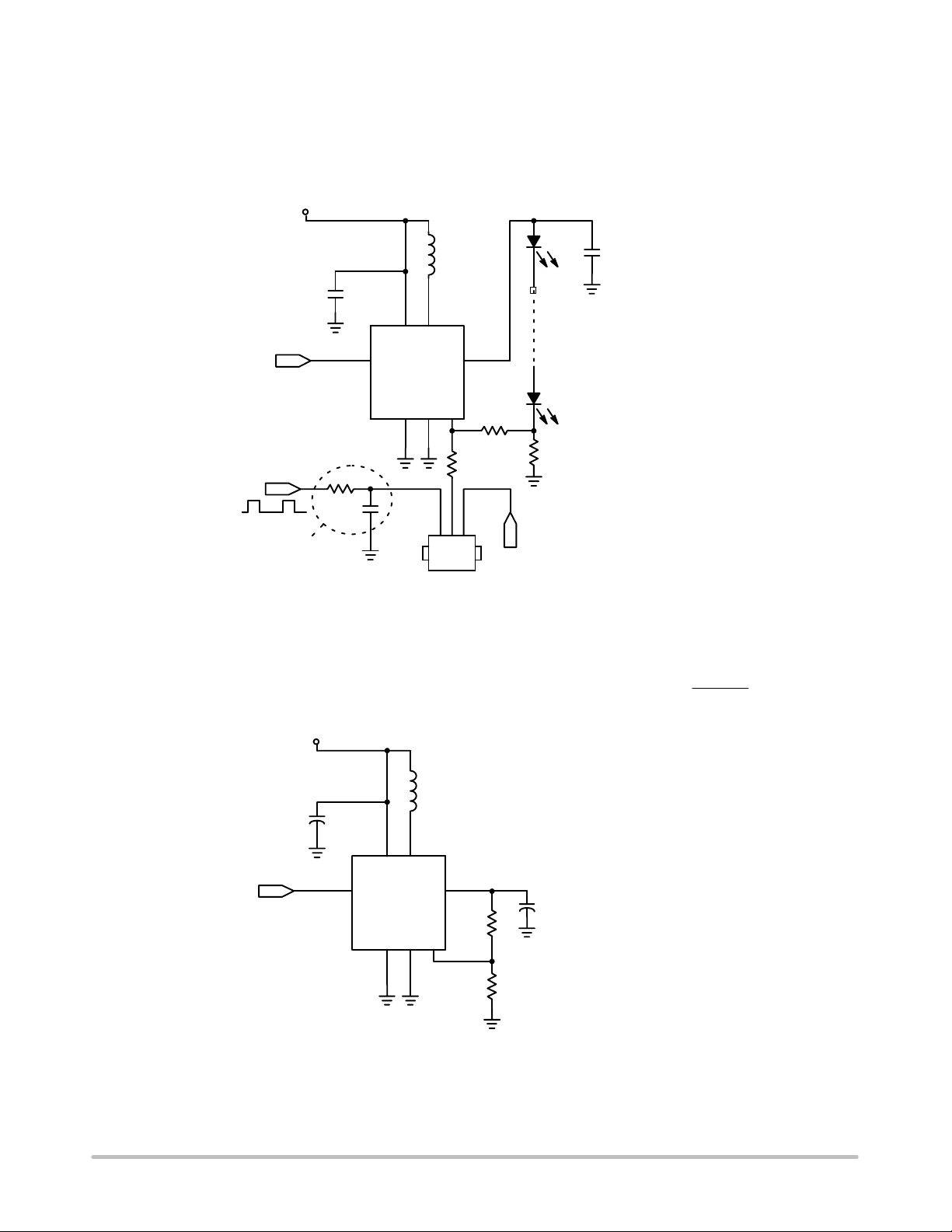
Analog Dimming Control
When the NCP5010 is in steady state the output voltage
is controlled in order to have 500 mV to the feedback input
(FB pin). The principle of this schematic is bias by a
resistive network R2/R3 the feedback voltage. If not any
V
Bat
2.7 to 5.5 V
22 mH
C1
4.7 mF 0603
ENABLE
PWM SIGNAL
Average Network
Figure 33. Dimming Control Using a Filtered PWM Signal or a DC Voltage
X5R 6.3 V
A2
NCP5010
R1 10 k
CTRL
IN
V
AGND
A1 B1
C3
470 nF
C2
SW
V
OUT
PGND
C3
Select
L1
signal is put from outside to R2 there is no voltage drop
across R3 and I
= VFB/R4. When the voltage put to R2
OUT
is increasing the loop balance output voltage to get always
500 mV to FB pin. Thereby voltage across R4 decreases
like this the current in the string of LEDs.
C2
1 mF 0805
X5R 25 V
2 to 5 LEDs
L1: TDK VLF4012A T−220MR51
C1: TDK C1608X5R0J475MT
C2: TDK C2012X5R1E105MT
C3: Standard Capacitor
FB
B3
R2
100 k
C1
R3
18 k
DC VOLTAGE
LED
LED
R4
24
DC/DC Boost Application
The NCP5010 can be used as DC/DC Boost converter to
deliver constant voltage to powering load like OLED or
V
Bat
2.7 to 5.5 V
L1
IN
V
AGND
A1 B1
C2
SW
V
OUT
PGND
C3
22 mH
FB
B3
C1
4.7 mF 0603
X5R 6.3 V
ENABLE
A2
CTRL
NCP5010
Figure 34. OLED or LCD Bias Supply
LCD biasing. An external resistive network is connected to
sense the output voltage and close the loop.
R1 ) R2
C1
R
290 k
R
10 k
15 V / 35 mA
C2
2.2 mF 0805
X5R 25 V
V
+ 0.5
out
L1: TDK VLF4012A T−220MR51
C1: TDK C1608X5R0J475MT
C2: TDK C2012X5R1E225MT
ǒ
R1
Ǔ
http://onsemi.com
15

NCP5010
ORDERING INFORMATION
Device Marking Operating T emperature Range Package Shipping
NCP5010FCT1G DAX −40°C to +85°C 8−Pin Flip−Chip CSP
(Pb−Free)
†For information on tape and reel specifications, including part orientation and tape sizes, please refer to our Tape and Reel Packaging
Specifications Brochure, BRD8011/D.
3000 Tape and Reel
†
Two type of demo boards available:
• The NCP5010EVB board which configures the device driving a string of 2−5 White LEDs in series.
• The NCP5010BIASEVB board for applications such as powering an OLED panel or LCD biasing.
Finally in addition to these demo boards, Application Note “ANDXXXX/D” deals with configuring the NCP5010 with a
high side sense resistor.
http://onsemi.com
16
NCP5010
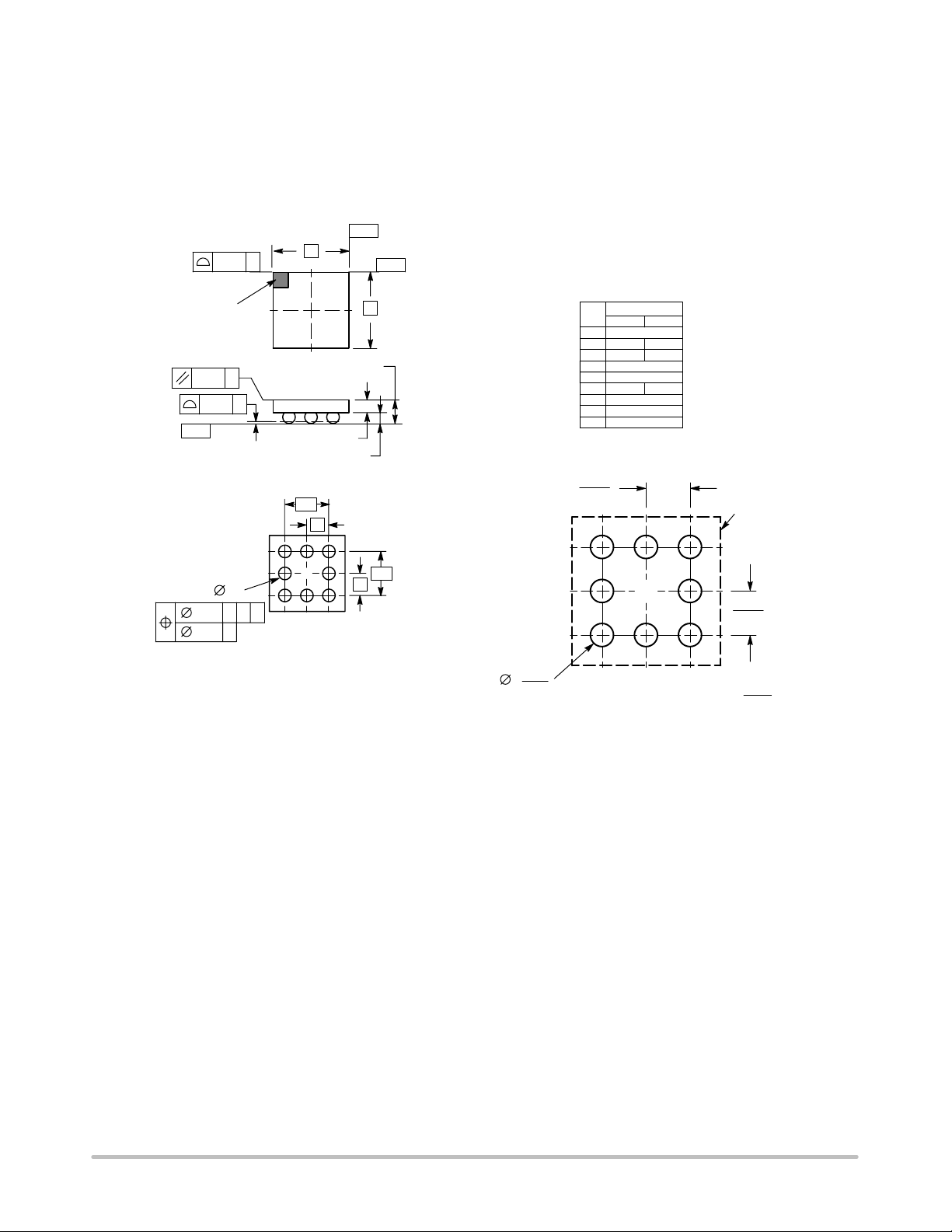
PACKAGE DIMENSIONS
8−PIN FLIP−CHIP
FC SUFFIX
CASE 499AJ−01
ISSUE A
PIN 1
INDICATOR
0.10 C
0.05 C
−C−
SEATING
PLANE
8X b
0.05 C
0.03 C
4 X
0.10 C
A B
D
TOP VIEW
SIDE VIEW
D1
e
C
B
A
12 3
BOTTOM VIEW
A2
−A−
A1
e
NOTES:
1. DIMENSIONING AND TOLERANCING PER
ANSI Y14.5M, 1982.
−B−
E
A
2. CONTROLLING DIMENSION: MILLIMETERS.
3. COPLANARITY APPLIES TO SPHERICAL
CROWNS OF SOLDER BALLS.
MILLIMETERS
DIM MIN MAX
A 0.6 BSC
A1 0.210 0.270
A2
0.330 0.390
D 1.70 BSC
E
1.70 BSC
b 0.290 0.340
e 0.500 BSC
D1 1.000 BSC
E1 1.000 BSC
SOLDERING FOOTPRINT
0.50
E1
0.265
0.01
0.0197
SCALE 20:1
DIE SIZE MAY VARY
0.50
0.0197
mm
ǒ
Ǔ
inches
http://onsemi.com
17

NCP5010
ON Semiconductor and are registered trademarks of Semiconductor Components Industries, LLC (SCILLC). SCILLC reserves the right to make changes without further notice
to any products herein. SCILLC makes no warranty, representation or guarantee regarding the suitability of its products for any particular purpose, nor does SCILLC assume any
liability arising out of the application or use of any product or circuit, and specifically disclaims any and all liability, including without limitation special, consequential or incidental
damages. “Typical” parameters which may be provided in SCILLC data sheets and/or specifications can and do vary in different applications and actual performance may vary over
time. All operating parameters, including “Typicals” must be validated for each customer application by customer’s technical experts. SCILLC does not convey any license under
its patent rights nor the rights of others. SCILLC products are not designed, intended, or authorized for use as components in systems intended for surgical implant into the body,
or other applications intended to support or sustain life, or for any other application in which the failure of the SCILLC product could create a situation where personal injury or death
may occur. Should Buyer purchase or use SCILLC products for any such unintended or unauthorized application, Buyer shall indemnify and hold SCILLC and its officers, employees,
subsidiaries, affiliates, and distributors harmless against all claims, costs, damages, and expenses, and reasonable attorney fees arising out of, directly or indirectly, any claim of
personal injury or death associated with such unintended or unauthorized use, even if such claim alleges that SCILLC was negligent regarding the design or manufacture of the part.
SCILLC is an Equal Opportunity/Affirmative Action Employer. This literature is subject to all applicable copyright laws and is not for resale in any manner.
PUBLICATION ORDERING INFORMATION
LITERATURE FULFILLMENT:
Literature Distribution Center for ON Semiconductor
P.O. Box 5163, Denver, Colorado 80217 USA
Phone: 303−675−2175 or 800−344−3860 Toll Free USA/Canada
Fax: 303−675−2176 or 800−344−3867 Toll Free USA/Canada
Email: orderlit@onsemi.com
N. American Technical Support: 800−282−9855 Toll Free
USA/Canada
Europe, Middle East and Africa Technical Support:
Phone: 421 33 790 2910
Japan Customer Focus Center
Phone: 81−3−5773−3850
http://onsemi.com
ON Semiconductor Website: www.onsemi.com
Order Literature: http://www.onsemi.com/orderlit
For additional information, please contact your local
Sales Representative
NCP5010/D
18
 Loading...