

Page 1

NCP1526
l
3 MHz, 400 mA,
High−Efficiency, Step−Down
Converter with Low Noise
Voltage Regulator Optimized
to Power Application
Processor or RF Module
The NCP1526 is a monolithic integrated circuit combining a
step−down PWM DC−DC converter and a low noise, low dropout
voltage regulator. The device is dedicated to power RF sensitive
module in portable applications from one Li−ion or three Alkaline /
NiCd / NiMH batteries cells. The DC−DC converter offers fixed
output voltage and delivers up to 400 mA. It uses synchronous
rectification to increase efficiency and eliminates the external
Schottky diode.
The device also has a built−in 3.0 MHz (nominal) oscillator which
reduces component size by allowing the use of small inductor (down
to 1 mH) and capacitors. Additional features include integrated
soft−start, cycle−by−cycle current limiting, and thermal shutdown
protection. The integrated very low noise, low dropout regulator is
available with 150 mA current capability, current limitation and
temperature limit protection.
The NCP1526 is available in a space saving, ultra low profile
3x3 mm, 10 pin UDFN package (thickness 0.55 mm max).
Features
• Step−Down Converter
− Up to 94% Efficiency (85% at 1.2 V)
− Output Current Capability 400 mA
− 3.0 MHz Switching Frequency
− Fixed Output Voltage (1.2 V available now, other voltages
available upon request) (see page 13)
− Synchronous Rectification for Higher Efficiency
• LDO Regulator
− Fixed Output Voltage (2.8 V available now, other voltages
available upon request) (see page 13)
− Up to 150 mA Output Current Capability
− Very Low Noise: 45 mV
• All Pins are Fully ESD Protected
• 2.7 V to 5.2 V Input Voltage Range
• Thermal Limit Protection
• 3.0 mm x 3.0 mm x 0.55 mm UDFN Package
• This is a Pb−Free Device
RMS
http://onsemi.com
MARKING
DIAGRAM
10 PIN DFN
MU SUFFIX
CASE 506AT
1526 = Specific Device Code
A = Assembly Location
L = Wafer Lot
Y = Year
W = Work Week
G = Pb−Free Package
(Note: Microdot may be in either location)
PIN CONNECTIONS
FB
EN1
EN2
GND2
BYPASS
(Top View)
ORDERING INFORMATION
Device Package Shipping
NCP1526MUTXG UDFN−10
(Pb−Free)
†For information on tape and reel specifications,
including part orientation and tape sizes, please
refer to our Tape and Reel Packaging Specification
Brochure, BRD8011/D.
1526
ALYWG
G
VIN1
LX
GND1
VIN2
V1
3000/Tape & Ree
†
T ypical Applications
• Cellular Phones, Smart Phones and PDAs
• Digital Still Cameras
• MP3 Players and Portable Audio Systems
• Wireless and DSL Modems
• Portable Equipment
© Semiconductor Components Industries, LLC, 2006
November, 2006 − Rev . 2
1 Publication Order Number:
NCP1526/D
Page 2
NCP1526
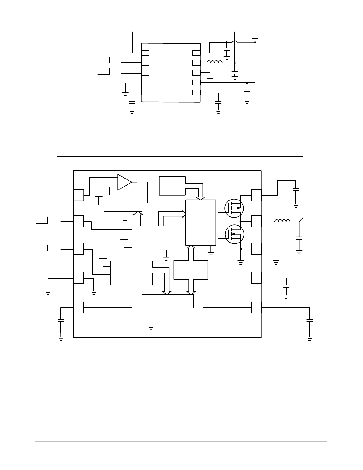
Vbattery
OFF ON
OFF ON
FB
EN1
EN2
C1
L1
V
BUCK
out
C5
V
LDO
out
C4
C3
OFF ON
OFF ON
C2
BUCK
LDO
1
2
3
4
5
FB
EN1
EN2
GND2
BYPASS
VIN1
LX
GND1
VIN2
V1
10
9
8
7
6
Figure 1. Typical Applications Circuit
Vbattery
ILIMIT
VIN1
1
2
3
REFERENCE
VIN2
VOLTAGE
VIN1
LOGIC
CONTROL
Buck Converter
PWM
CONTROL
Q1
Q2
10
9
8
VIN1
LX
GND1
4.7 mF
2.2 mH
4.7 mF
V
out
BUCK
1.20 V ,
400 mA
100 nF
GND2
BYPASS
LOGIC
4
5
CONTROL
LDO
V1 BLOCK
Thermal
Shutdown
Vbattery
VIN2
7
4.7 mF
V
LDO
out
V1
6
2.80 V , 150 mA
1 mF
Figure 2. Simplified Block Diagram
http://onsemi.com
2
Page 3
NCP1526
PIN FUNCTION DESCRIPTION (Pin out provided for concept purpose only and might change in the final product.)
Pin No. Symbol Function Description
1 FB Analog Input Feedback voltage from the output of the power supply. This is the input to
2 EN1 Digital Input Enable for DC−DC converter. This pin is active high. It is turned of f by logic
3 EN2 Digital Input EN2 enables the LDO.A HIGH level on this pin activates the voltage
4 GND2 Power Ground Ground connection for the LDO section and must be connected to the
5 BYPASS Bypass is the bandgap reference for the LDO. This pin requires a 100 nF
6 V1 Output Power This pin provides the output voltage supplied by the LDO. This pin requires
7 VIN2 Power Input Input battery voltage to supply voltage regulator blocks. The pin requires a
8 GND1 Power Ground This pin is the GROUND reference for the DC−DC converter and the output
9 LX Analog Output Connection from Power MOSFETs to the inductor. An output discharge
10 VIN1 Power Input Input battery voltage to supply the analog and digital blocks of the DC−DC
the error amplifier.
LOW on this pin. Do not float this pin.
regulator. It is turned off by logic LOW on this pin. Do not float this pin.
system ground.
bypass capacitor for low noise. This pin cannot be used for an external
source.
1.0 mF decoupling capacitor.
4.7 mF decoupling capacitor.
control. The pin must be connected to the system ground.
circuit sinks current from this pin.
converter. The pin must be decoupled to ground by a 4.7 mF ceramic
capacitor.
MAXIMUM RATINGS
Rating Symbol Value Unit
Minimum Voltage All Pins V
Maximum Voltage All Pins (Note 2) V
Maximum Voltage EN1, EN2, FB, LX V
UDFN10 Package (Note 5)
min
max
max
R
q
JA
Thermal Resistance, Junction−to−Air
Operating Ambient Temperature Range T
Storage Temperature Range T
Junction Operating Temperature T
Latch−up Current Maximum Rating (TA = 85°C) (Note 4) FB pin
A
stg
J
Lu "70
Latch−up Current Maximum Rating (TA = 85°C) (Note 4) Other pins
ESD Withstand Voltage (Note 3)
Vesd
Human Body Model
Machine Model
Stresses exceeding Maximum Ratings may damage the device. Maximum Ratings are stress ratings only. Functional operation above the
Recommended Operating Conditions is not implied. Extended exposure to stresses above the Recommended Operating Conditions may affect
device reliability.
1. Maximum electrical ratings are defined as those values beyond which damage to the device may occur at TA = 25°C.
2. According to JEDEC standard JESD22−A108B.
3. This device series contains ESD protection and exceeds the following tests:
Human Body Model (HBM) per JEDEC standard: JESD22−A114.
Machine Model (MM) per JEDEC standard: JESD22−A115.
4. Latchup current maximum rating per JEDEC standard: JESD78.
5. The exposed flag shall be connected to ground.
6. Moisture Sensitivity Level (MSL): 1 per IPC/JEDEC standard: J−STD−020A.
−0.3 V
7.0 V
VIN + 0.3 V
240 °C/W
−40 to 85 _C
−55 to 150 _C
−40 to 125 _C
mA
"100
2.0
kV
200
V
http://onsemi.com
3
Page 4

NCP1526
ELECTRICAL CHARACTERISTICS, DC/DC Converter (Typical values are referenced to T
= +25°C, Min and Max values are
A
referenced −40°C to +85°C ambient temperature, unless otherwise noted, operating conditions VIN = 3.6 V , unless otherwise noted.)
Characteristic Pin Symbol Min Typ Max Unit
VIN1 PIN
Input Voltage Range 10 V
Quiescent Current, I
Quiescent Current, I
Quiescent Current, EN Low 8 I
= 0 mA, No Switching
out
= 0 mA, Oscillator Running
out
8 I
q OFF
Undervoltage Lockout (VIN Increase) 10 V
Undervoltage Lockout Hysteresis 10 V
HUVLO
in
q ON
UVLO
2.7 − 5.2 V
−
−
250
2.5
350
−
− 0.2 1.5 mA
− 2.5 − V
− 100 − mV
EN1, EN2 PIN
Positive Going Input High Voltage Threshold, EN0 Signal 2, 3 V
Negative Going Input High Voltage Threshold, EN0 Signal 2, 3 V
IH
IL
1.2 − − V
− − 0.4 V
DC−DC CONVERTER SECTION
Peak Inductor Current 9 I
Feedback Voltage Threshold
1 V
Overtemperature
Load Transient Response, Rise/Fall Time 1.0 ms
− V
1.0 mA to 300 mA Load Step
1.0 mA to 400 mA Load Step
Line Transient Response, I
Output Voltage Load Regulation
I
= 1.0 mA to 300 mA
out
I
= 1.0 mA to 400 mA
out
Output Voltage Line Regulation, I
Output Voltage Ripple, I
= 100 mA, 3.0 V to 3.6 V Line Step − V
out
− V
= 100 mA, VIN = 2.7 V to 5.2 V − V
out
= 300 mA − V
out
Oscillator Frequency 9 F
LIM
FB
OUT
OUT
OUT
OUT
OUT
OSC
− 1000 − mA
1.164 1.2 1.236
−
−
30
35
−
−
− "5.0 − mVpp
−
−
0.2
0.5
−
−
− 0.1 − %
− 5.0 − mV
2.4 3.0 3.6 MHz
P−Ch On−Resistance 1 RLxH − 400 − mW
N−Ch On−Resistance 1 RLxL − 400 − mW
P−Ch Leakage Current 1 ILeakH − 0.05 − mA
N−Ch Leakage Current 1 ILeakL − 0.01 − mA
Soft−Start Time − Tstart − 100 300 ms
mA
mA
V
mV
%
http://onsemi.com
4
Page 5

NCP1526
ELECTRICAL CHARACTERISTICS for LDO (Typical values are referenced to T
= +25°C, Min and Max values are referenced
A
−40°C to +85°C ambient temperature, unless otherwise noted, operating conditions 3 V < VIN < 5.2 V , unless otherwise noted.)
Characteristic Pin Symbol Min Typ Max Unit
VIN2 PIN
Input Voltage Range 7 V
Quiescent Current On State
VIN2 = 4.2 V , I
out
= 0 mA
Quiescent Current Off State 4 I
4 I
q OFF
in
q ON
3 − 5.2 V
− 70 95 mA
− 0.2 − mA
LDO SECTION
Output Voltage, I
Maximum Output Current 6 I
Output Voltage Line Regulation, I
Load Regulation, I
Power Supply Ripple Rejection on V1, (0.2 Vp−p),
C
= 1.0 mF, Vin = 3.6 V
out
1.0 kHz I
out1
100 kHz, I
Dropout Voltage, I
= 0 mA to 150 mA 6 V1 2.716 2.80 2.884 V
out
out
= 10 mA 6 V1 − 10 − mV
out
= 1.0 mA to 150 mA, VIN = 3.6 V 6 V1 − 20 − mV
out
150 − − mA
6 PSRR
= 100 mA
= 100 mA
out1
= 150 mA VINA−V1 − − 150 mV
out
−
−
67
45
−
−
Output Short Circuit Current 6 ISC 250 300 − mA
Output Noise Voltage, 100 Hz to 100 kHz, I
= 10 mA, C
out
= 1.0 mF 6 V
out
N
− 45 − mVrms
Turn ON Output V oltage, Vin = 3.6 V 6 Ton − 80 150 ms
BYPASS PIN
Output Voltage, Cby = 100 nF 5 V
BY
− 1.5 − V
dB
http://onsemi.com
5
Page 6

NCP1526
T ABLE OF GRAPHS
TYPICAL CHARACTERISTICS FOR STEP DOWN CONVERTER FIGURE
h Efficiency
V
OUT
F
OSC
V
OUT
V
OUT
V
OUT
V
OUT
Tstart Soft Start 11
Output Voltage vs. Temperature 6
Frequency Variation vs. Input Voltage 7
Load Regulation vs. Load Current 5
Load Transient Response 12
Line Regulation
Line Transient Response 14
PWM Mode Operation 13
TYPICAL CHARACTERISTICS
NCP1526 circuit on Figure 2, Vin = 3.6 V , TA = 25°C, unless otherwise noted
vs. Load Current 3, 4
vs. Input Voltage 8
vs. Ouptput Current 9
vs. Temperature 10
100
90
Vin = 2.7 V
80
70
60
EFFICIENCY (%)
50
STEP DOWN CONVERTER
40
30
Figure 3. Step Down Converter Efficiency vs.
3.0
2.0
1.0
0
−1.0
LOAD REGULATION (%)
STEP DOWN CONVERTER
−2.0
100
90
Vin = 3.6 V
Vin = 5.2 V
4003002001000
I
, OUTPUT CURRENT (mA) I
out
80
70
60
EFFICIENCY (%)
50
STEP DOWN CONVERTER
40
30
Figure 4. Step Down Converter Efficiency vs.
Output Current
1.225
TA = 25°C
TA = −40°C
1.215
TA = 85°C
Vin = 3.6 V
1.205
Temperature V
Vin = 2.7 V
Vin = 5.2 V
TA = 25°C
(mA)
out
= 3.6 V
in
TA = −40°C
TA = 85°C
4003002001000
−3.0
I
(mA) TEMPERATURE (°C)
out
Figure 5. Step Down Converter Load
Regulation vs. Temperature V
= 3.6 V
in
1.195
4003002001000
STEP DOWN CONVERTER OUTPUT VOLTAGE (V)
http://onsemi.com
6
Figure 6. Step Down Converter Output Voltage
vs. T emperature at I
= 100 mA
out
1251007550250−25−50
Page 7

NCP1526
5.0
4.0
3.0
2.0
1.0
0
−1.0
−2.0
−3.0
FREQUENCY VARIATION (%)
−4.0
−5.0
I
= 100 mA
out
Vin, INPUT VOLTAGE (V) Vin, INPUT VOLTAGE (V)
Figure 7. Step Down Converter Switching
Frequency vs. Input Voltage
5.24.74.23.73.22.7
100
90
80
70
60
EFFICIENCY (%)
50
40
30
TA = 25°C
Figure 8. Step Down Converter Efficiency vs.
Input Voltage at I
= 100 mA
out
TA = −40°C
TA = 85°C
5.55.04.54.03.53.02.5
http://onsemi.com
7
Page 8
NCP1526
TYPICAL CHARACTERISTICS
NCP1526 circuit on Figure 2, Vin = 3.6 V , TA = 25°C, unless otherwise noted
2.0
1.0
0
−1.0
LINE REGULATION (%)
−2.0
I
out
I
out
I
out
Vin, (V) Vin (V)
Figure 9. Step Down Converter Line
Regulation vs. Output Current
V
EN
1 V / Div
= 400 mA
= 100 mA
= 0.1 mA
1.0
0.5
TA = −40°C
0
−0.5
LINE REGULATION (%)
TA = 25°C
TA = 85°C
−1.0
5.24.74.23.73.22.7
5.24.74.23.73.22.7
Figure 10. Step Down Converter Line
Regulation vs. Temperature at I
I
out
200 mA / Div
= 100 mA
out
V
out
500 mV / Div
20 ms / Div
Figure 11. Step Down Converter
Soft Start Time
I
out
10 ms / Div
200 mA / Div
V
LX
2 V / Div
V
in
2 V / Div
V
out
10 mV / Div
V
out
20 mV / Div
40 ms / Div
Figure 12. Step Down Converter Load
Transient Response
V
in
200 mV / Div
V
out
10 mV / Div
100 ms / Div
Figure 13. Step Down Converter PWM Mode of
Operation
Figure 14. Step Down Converter Line Transient
Response
http://onsemi.com
8
Page 9

NCP1526
T ABLE OF GRAPHS
TYPICAL CHARACTERISTICS FOR LDO FIGURE
VINA−V1 Dropout vs. Load Current 22
V1 Load Regulation vs. Load Current 15, 16
Load Transient Response 18
Iq
ON
T
ON
V
N
PSRR PSRR vs. Frequency 23
Quiescent Current vs. Input Voltage 19
Turn On Time 17
LDO Noise vs. Frequency 20, 21
TYPICAL CHARACTERISTICS
NCP1526 circuit on Figure 2, Vin = 3.6 V , TA = 25°C, unless otherwise noted
1.0
0.6
0.2
−0.2
LOAD REGULATION (%)
−0.6
−1.0
1.0
0.5
TA = 85°C
Vin = 2.7 V
Vin = 5.2 V
Vin = 3.6 V
TA = 25°C
0
TA = −40°C
−0.5
LOAD REGULATION (%)
−1.0
150100500
I
, OUTPUT CURRENT (mA) I
out
out
, (mA)
Figure 15. LDO Load Regulation Figure 16. LDO Load Regulation vs.
Temperature
I
V
out
1 V / Div
out
200 mA / Div
1501209060300
EN
2 V / Div
100 ms / Div
V
out
20 mV / Div
10 ms / Div
Figure 17. LDO Turn On Time from Enable Figure 18. LDO Load Transient Response
http://onsemi.com
9
Page 10
NCP1526
100
QUIESCENT CURRENT (mA)
1,000
100
NOISE (mV/√Hz)
1.0
10,000
Band Power
90
80
70
60
50
3.4 4.84.64.4
Vin (V) FREQUENCY (Hz)
Figure 19. LDO Quiescent Current vs. Input
1,000
NOISE (mV/√Hz)
5.25.04.24.03.83.63.23.0
100 Hz to 100 KHz: 17 mVrms
100
10
Figure 20. LDO Noise (DC/DC Converter Off)
Voltage
TYPICAL CHARACTERISTICS
NCP1526 circuit on Figure 2, Vin = 3.6 V , TA = 25°C, unless otherwise noted
100
90
80
70
60
50
10
Band Power
100 Hz to 100 KHz: 27 mVrms
100,00010,0001,000100
FREQUENCY (Hz) I
40
DROPOUT (mV)
30
20
10
0
Figure 21. LDO Noise (DC/DC Converter On) Figure 22. LDO Dropout Voltage vs. Output
TA = 25°C
, (mA)
out
Current
100,00010,0001,000100
TA = −40°C
TA = 85°C
1501209060300
20
10
0
−10
−20
−30
−40
GAIN (dB)
−50
−60
−70
−80
−90
Figure 23. LDO PSRR at I
(Hz)
= 100 mA, Vin = 3.6 V
out
http://onsemi.com
10
1,000,000100,00010,0001,00010010
Page 11
NCP1526
DC−DC OPERATION DESCRIPTION
Detailed Description
The NCP1526 uses a constant frequency, voltage mode
step−down architecture. Both the main (P−Channel
MOSFET) and synchronous (N−Channel MOSFET)
switches are internal.
It delivers a constant voltage from either a single Li−Ion
or three cell NiMH/NiCd battery to portable devices such
as cell phones and PDA. The output voltage accuracy is
well within 3% of the 1.20 V. The NCP1526 can source at
least 400 mA.
PWM Operating Mode
The output voltage of NCP1526 is regulated by
modulating the on−time pulse width of the main switch Q1
3.6040
3.6000
3.5960
400 m
200 m
400 m
300 m
200 m
0.00
V
in
I
PFET
I
L
at a fixed 3.0 MHz frequency. The switching of the PMOS
Q1 is controlled by a flip−flop driven by the internal
oscillator and a comparator that compares the error signal
from an error amplifier with the PWM ramp. At the
beginning of each cycle, the main switch Q1 is turned ON
by the rising edge of the internal oscillator clock. When the
PWM ramp becomes higher than the error voltage
amplifier the PWM comparator resets the flip−flop, Q1 is
turned OFF and the synchronous switch Q2 is turned ON.
Q2 replaces the external Schottky diode to reduce the
conduction loss and improve the efficiency. To avoid
overall power loss, a certain amount of dead time is
introduced to ensure Q1 is completely turned OFF before
Q2 is being turned ON.
I
3.70
1.35
NFET
V
O
V
LX
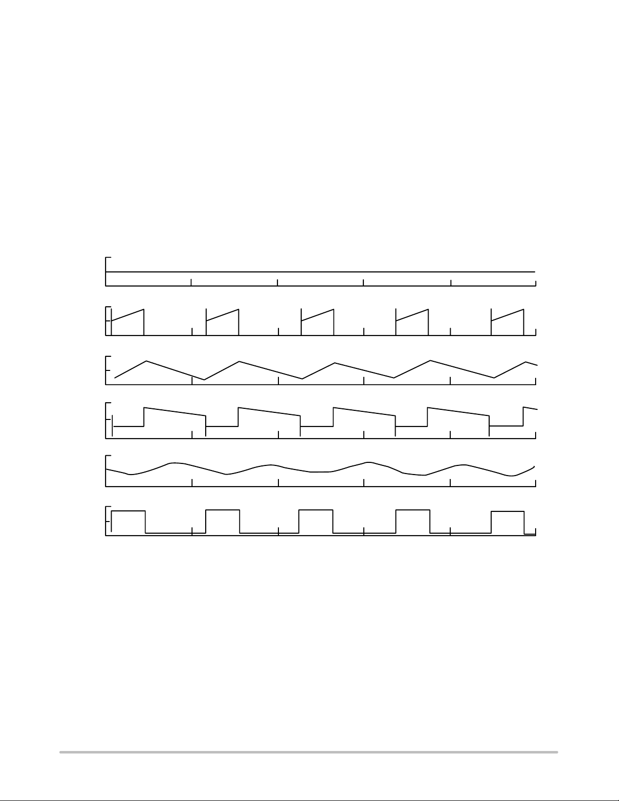
Figure 24. Waveforms During PWM Operation
400 m
100 m
−200 m
1.205
1.200
1.195
−1.00
Soft−Start
The NCP1526 uses soft−start to limit the inrush current
when the device is initially powered up or enabled.
Soft−start is implemented by gradually increasing the
reference voltage until it reaches the full reference voltage.
During startup, a pulsed current source charges the internal
soft−start capacitor to provide gradually increasing
reference voltage. When the voltage across the capacitor
ramps up to the nominal reference voltage, the pulsed
current source will be switched off and the reference
voltage will switch to the regular reference voltage.
Cycle−by−Cycle Current Limitation
From the block diagram (Figure 2), an ILIM comparator
is used to realize cycle−by−cycle current limit protection.
The comparator compares the LX pin voltage with the
reference voltage, which is biased by a constant current. If
the inductor current reaches the limit, the ILIM comparator
detects the LX voltage falling below the reference voltage
and releases the signal to turn off the switch Q1. The
cycle−by−cycle current limit is set at 1000 mA (nom).
http://onsemi.com
11
Page 12

NCP1526
Shutdown Mode
When the EN1 pin has a voltage applied of less than
0.4 V, the DC−DC converter block will be disabled. In
shutdown mode, the internal reference, oscillator and most
of the control circuitries are turned off. Therefore, the
typical current consumption will be 0.2 mA (typical value).
Applying a voltage above 1.2 V to EN1 pin will enable the
DC−DC converter for normal operation. The device will go
through soft−start to normal operation.
Thermal Shutdown
Internal Thermal Shutdown circuitry is provided to
protect the integrated circuit in the event that the maximum
junction temperature is exceeded. If the junction
temperature exceeds 160_C, the device shuts down. In this
mode switch Q1 and Q2 and the control circuits are all
turned off. The device restarts in soft−start after the
temperature drops below 135°C. This feature is provided
to prevent catastrophic failures from accidental device
overheating and it is not intended as a substitute for proper
heatsinking.
Undervoltage Lockout
The input voltage VIN1 must reach 2.5 V (typ) before the
NCP1526 enables the DC−DC converter output to begin
the startup sequence (see soft−start section). The UVLO
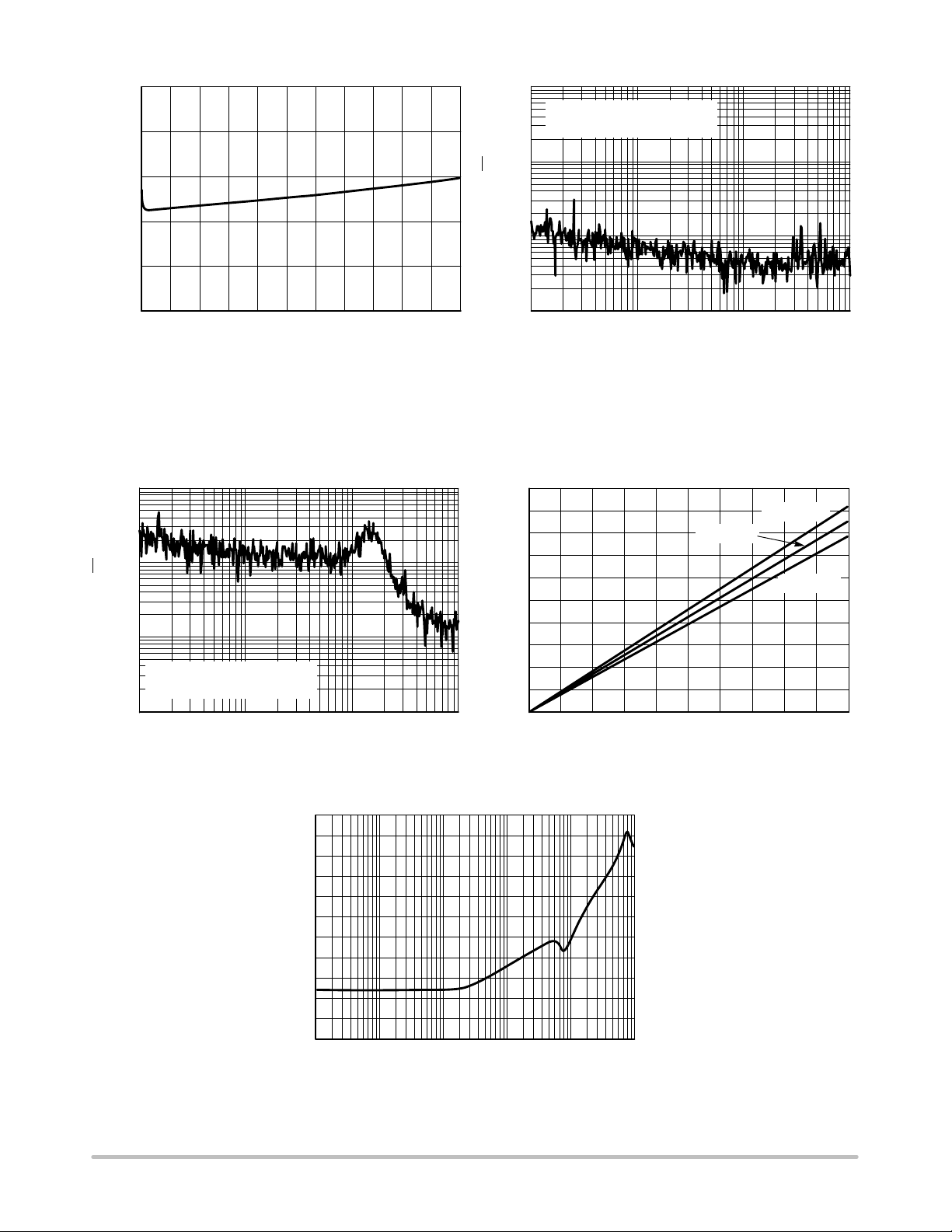
threshold hysteresis is typically 100 mV.
Due to the nature of the buck converter, the output L−C
filter must be selected to work with internal compensation.
For NCP1526, the internal compensation is internally fixed
and it is optimized for an output filter of L = 2.2ĂmH and
C
= 4.7ĂmF
OUT
The corner frequency is given by:
f
+
c
1
Ǹ
2p L C
+
2p 2.2 mH 4.7 mF
out
1
Ǹ
+ 49.5 KHz
The device operates with inductance value between 1 mH
and maximum of 4.7 mH.
If the corner frequency is moved, it is recommended to
check the loop stability depending of the output ripple
voltage accepted and output current required. For lower
frequency, the stability will be increase; a larger output
capacitor value could be chosen without critical effect on
the system. On the other hand, a smaller capacitor value
increases the corner frequency and it should be critical for
the system stability. Take care to check the loop stability.
The phase margin is usually higher than 45°.
Table 2. L−C Filter Example
Inductance (L) Output Capacitor (C
1 mH 10 mF
2.2 mH 4.7 mF
4.7 mH 2.2 mF
out
)
APPLICATION INFORMATIONS
Input Capacitor Selection
In PWM operating mode, the input current is pulsating
with large switching noise. Using an input bypass capacitor
can reduce the peak current transients drawn from the input
supply source, thereby reducing switching noise
significantly. The capacitance needed for the input bypass
capacitor depends on the source impedance of the input
supply.
The maximum RMS current occurs at 50% duty cycle
with maximum output current, which is IO, max/2.
For NCP1526, a low profile ceramic capacitor of 4.7 mF
should be used for most of the cases. For effective bypass
results, the input capacitor should be placed as close as
possible to the VIN Pin.
Table 1. List of Input Capacitors
Murata
Taiyo Yuden JMK212BY475MG
TDK
GRM188R60J475KE
GRM21BR71C475KA
C2012X5ROJ475KB
C1632X5ROJ475KT
Inductor selection
The inductor parameters directly related to device
performances are saturation current and DC resistance and
inductance value. The inductor ripple current (DIL)
decreases with higher inductance:
DI
V
out
+
L
L f
sw
ǒ
1 *
V
out
Ǔ
V
in
DIL peak to peak inductor ripple current
L inductor value
fsw Switching frequency
The Saturation current of the inductor should be rated
higher than the maximum load current plus half the ripple
current:
DI
I
L(MAX)
+ I
O(MAX)
)
L
2
IL(MAX) Maximum inductor current
IO(MAX) Maximum Output current
The inductor’s resistance will factor into the overall
efficiency of the converter. For best performances, the DC
resistance should be less than 0.3 W for good efficiency.
Output L−C filter Design Considerations:
The NCP1526 is built in 3ĂMHz frequency and uses
voltage mode architecture. The correct selection of the
output filter ensures good stability and fast transient
response.
http://onsemi.com
12
Page 13

NCP1526
Table 3. List of Inductors
FDK MIPW3226 series
TDK
Taiyo Yuden LQ CBL2012
Coil craft
Output capacitor selection
VLF3010AT series
TFC252005 series
DO1605−T series
LPO3008
Selecting the proper output capacitor is based on the
desired output ripple voltage. Ceramic capacitors with low
ESR values will have the lowest output ripple voltage and
are strongly recommended. The output capacitor requires
either an X7R or X5R dielectric.
The output ripple voltage in PWM mode is given by:
DV
+ DI
out
Table 4. List of Output Capacitors
Murata GRM188R60J475KE 4.7 mF
Taiyo Yuden JMK212BY475MG 4.7 mF
TDK C2012X5ROJ475KB 4.7 mF
OUTPUT VOLTAGE OPTIONS AVAILABLE UPON
REQUEST
Fixed Output Voltage (V)
ǒ
L
GRM21BR71C475KA
GRM188R60OJ106ME 10 mF
JMK212BJ106MG 10 mF
C1632X5ROJ475KT
C2012X5ROJ106K 10 mF
DC/DC Converter
1
4 fsw C
out
) ESR
0.9
1.0
1.1
1.2
1.3
1.4
1.5
1.6
1.7
1.8
1.9
2.5
2.7
3.0
3.3
Ǔ
LDO Operation
Voltage Regulator V1
V1 is a 2.80 V, 3% low drop voltage regulator dedicated
to RF sensitive module. It can deliver up to 150 mA and is
totally protected against short to ground (current
limitation) and overtemperature (thermal shutdown circuit
with hysteresis).
The PSRR of the reference is in excess of 67 dB at
1.0 kHz. The output of the V1 requires a 1.0 mF capacitor
for stability. An additional 100 nF capacitor is necessary on
the BYPASS pin for a low output noise. If the BYPASS pin
is supporting an additional load, the stability and
performance of the V1 will be diminished. Since the input
voltage can go as low as 3.0 V, the reference output will be
affected and can drop as low as 150 mV below the input
voltage at 150 mA output current. During this low dropout,
the PSRR of the reference is reduced. V1 is active when
logic high is applied to the EN2 pin. It is turned off by a
logic low on the EN2 pin.
Reference Bypass Capacitor Node (Bypass)
An optional 100 nF BYP ASS capacitor creates a low pass
filter for LDO noise reduction. The output voltage noise is
45 mV
RMS
with C
BYPASS
= 0.1 mF and C
= 1.0 mF. If the
OUT
BYPASS pin is supporting an additional load, the stability
and performance of the NCP1526 will be diminished.
Current Limiting
The output voltage regulator limits the output current to
I
= 300 mA (typ). If the LDO output current exceeds I
SC
SC
the output voltage drops.
Shutdown Mode
When the EN2 pin has a voltage applied of less than
0.4 V, the output voltage regulator will be disabled. In
shutdown mode, the internal reference and most of the
control circuitries are turned off. Therefore, the typical
current consumption will be 0.2 mA (typical value).
Applying a voltage above 1.2 V to EN2 pin will enable the
LDO for normal operation.
OUTPUT VOLTAGE OPTIONS AVAILABLE UPON
REQUEST
LDO
2.5
2.6
2.7
Fixed Output Voltage (V)
2.8
2.85
3.0
3.1
3.3
,
http://onsemi.com
13
Page 14

NCP1526
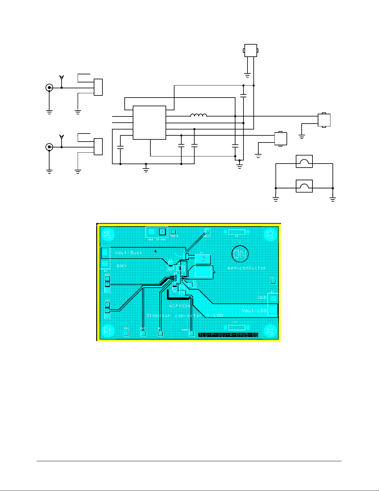
APPLICATION BOARD
PCB Layout Recommendations
Good PCB layout plays an important role in switching
mode power conversion. Careful PCB layout can help to
minimize ground bounce, EMI noise and unwanted
feedback that can affect the performance of the converter.
Hints suggested below can be used as a guideline in most
situations.
1. Use star−ground connection to connect the IC
ground nodes and capacitor GND nodes together
at one point. Keep them as close as possible, and
then connect this to the ground plane through
several vias. This will reduce noise in the ground
plane by preventing the switching currents from
flowing through the ground plane.
2. Place the power components (i.e., input capacitor,
inductor and output capacitor) as close together
as possible for best performance. All connecting
traces must be short, direct, and wide to reduce
voltage errors caused by resistive losses through
the traces.
3. Separate the feedback path of the output voltage
from the power path. Keep this path close to the
NCP1526 circuit. And also route it away from
noisy components. This will prevent noise from
coupling into the voltage feedback trace.
The following shows the NCP1526 demo board
schematic and layout and bill of materials:
V
battery
OFF ON
OFF ON
BUCK
LDO
LX
GND1
VIN2
V1
10
9
8
7
V
out
6
1
FB VIN1
2
EN1
3
EN2
4
GND2
5
BYPASS
Figure 25. NCP1526 Board Schematic
LDO
C1
L1
V
BUCK
out
C3C2
C5
C4
Figure 26. NCP1526 Board Layout
http://onsemi.com
14
Page 15
EN1
T POINT A
J9
en2
BNC H
0
EN2
T POINT A
J12
en2
BNC H
0
NCP1526
J5
HEADER 2
12
V
V
in
J10
1
2
3
CON3
0
V
in
J13
1
2
3
en1
en2
bp
100 n
U1
1
FB
2
EN1
3
EN2
4
GND2
BYPASS5V1
C2
NCP1526
VIN1
LX
GND1
VIN2
EP
11
10
2.2 mH
L1
lx
9
8
7
V
C3
1 m
out
2
C4
4.7 m
6
4.7 m
C5
4.7 m
CON3
0
0
Figure 27. Schematics
in
0
C1
V
1
out
HEADER 2
1
J8
2
J6
0
12
HEADER 2
1
2
J7
0
0
JUMPER1
J11
12
JUMPER1
0
0
Figure 28. Board Layout (Top View)
http://onsemi.com
15
Page 16

NCP1526
Figure 29. Board Layout (Bottom View)
BILL OF MATERIALS
Designator Qty Description Value Tolerance Footprint Manufacturer Manufacturer
U1 1 IC, Converter,
C1, C4, C5 3 Ceramic Capacitor 4.7 mF,
C3 1 Ceramic Capacitor 1 mF,
C2 1 Ceramic Capacitor 100 nF,
L1 1 Inductor 2.2 mH 20% 1605 Coilcraft DO1605T−222MLB
J5, J6, J7 2 Male
J10, J13 1 3 Pin Jumper
J11, J8 2 Jumper for GND NA NA 10.16 mm Harwin D3082−01
EN1, EN2,
VOUT_LDO,
LX, TPVIN,
VOUT_BUCK
J9, J12 0* SMB Connector NA NA NA Radiall R114665000
1 88.9x61.1x1.6mm
*G1 is not connected on the evaluation board.
6 Test Point NA NA NA Std Std
DC/DC
SL5.08/2/90B +
Female
BLZ5.08/2/90B
Connector I/O
Header
4 Layers
NA NA 10−Pin
DFN
10% 0805 Murata GRM219R61A475KE19
10 V , X5R
20% 0805 Murata GNM212R61A105MA13
6.3 V , X5R
10% 0805 Murata GRM219R71C104KA01
10 V , X7R
NA NA NA Weidmuller 1510360000
NA NA 2.54 mm TYCO/AMP 5−826629−0
NA NA NA Any TLS−P−002−A−0606−DA
ON
Semiconductor
Part Number
NCP1526
1555060000
+
http://onsemi.com
16
Page 17

10X
REFERENCE
2X
2X
0.10 C
0.08 C
PIN ONE
0.15 C
10X
0.15 C
L
NCP1526
PACKAGE DIMENSIONS
10 PIN UDFN
CASE 506AT−01
ISSUE O
D
D2
1
5
A1
e
A3
A
B
E
A
SEATING
C
PLANE
8X
NOTES:
1. DIMENSIONING AND TOLERANCING PER
ASME Y14.5M, 1994.
2. CONTROLLING DIMENSION: MILLIMETERS.
3. DIMENSION b APPLIES TO PLATED
TERMINAL AND IS MEASURED BETWEEN
0.25 AND 0.30mm FROM TERMINAL.
4. COPLANARITY APPLIES TO THE EXPOSED
PAD AS WELL AS THE TERMINALS.
DIMAMIN NOM MAX
A1 0.00 0.03 0.05
A3 0.127 REF
b 0.18 0.25 0.30
D 3.00 BSC
D2 2.40 2.50 2.60
E 3.00 BSC
E2
e 0.50 BSC
K
L
MILLIMETERS
0.45 0.50 0.55
1.70 1.80 1.90
0.19 TYP
0.30 0.40 0.50
SOLDERING FOOTPRINT*
2.6016
2.1746
1.8508
3.3048
E2
10X
K 10
6
b
10X
A0.10 C
B
0.05 C
NOTE 3
10X
0.5651
10X
0.3008
0.5000 PITCH
DIMENSIONS: MILLIMETERS
*For additional information on our Pb−Free strategy and soldering
details, please download the ON Semiconductor Soldering and
Mounting T echniques Reference Manual, SOLDERRM/D.
ON Semiconductor and are registered trademarks of Semiconductor Components Industries, LLC (SCILLC). SCILLC reserves the right to make changes without further notice
to any products herein. SCILLC makes no warranty, representation or guarantee regarding the suitability of its products for any particular purpose, nor does SCILLC assume any
liability arising out of the application or use of any product or circuit, and specifically disclaims any and all liability, including without limitation special, consequential or incidental
damages. “Typical” parameters which may be provided in SCILLC data sheets and/or specifications can and do vary in different applications and actual performance may vary over
time. All operating parameters, including “Typicals” must be validated for each customer application by customer’s technical experts. SCILLC does not convey any license under
its patent rights nor the rights of others. SCILLC products are not designed, intended, or authorized for use as components in systems intended for surgical implant into the body,
or other applications intended to support or sustain life, or for any other application in which the failure of the SCILLC product could create a situation where personal injury or death
may occur. Should Buyer purchase or use SCILLC products for any such unintended or unauthorized application, Buyer shall indemnify and hold SCILLC and its officers, employees,
subsidiaries, affiliates, and distributors harmless against all claims, costs, damages, and expenses, and reasonable attorney fees arising out of, directly or indirectly, any claim of
personal injury or death associated with such unintended or unauthorized use, even if such claim alleges that SCILLC was negligent regarding the design or manufacture of the part.
SCILLC is an Equal Opportunity/Affirmative Action Employer. This literature is subject to all applicable copyright laws and is not for resale in any manner.
PUBLICATION ORDERING INFORMATION
LITERATURE FULFILLMENT:
Literature Distribution Center for ON Semiconductor
P.O. Box 5163, Denver, Colorado 80217 USA
Phone: 303−675−2175 or 800−344−3860 Toll Free USA/Canada
Fax: 303−675−2176 or 800−344−3867 Toll Free USA/Canada
Email: orderlit@onsemi.com
N. American Technical Support: 800−282−9855 Toll Free
USA/Canada
Europe, Middle East and Africa Technical Support:
Phone: 421 33 790 2910
Japan Customer Focus Center
Phone: 81−3−5773−3850
http://onsemi.com
17
ON Semiconductor Website: www.onsemi.com
Order Literature: http://www.onsemi.com/orderlit
For additional information, please contact your local
Sales Representative
NCP1526/D
 Loading...