

Page 1
查询NCP1030供应商
NCP1030, NCP1031
Low Power PWM Controller
with On−Chip Power Switch
and Startup Circuits for
48V Telecom Systems
The NCP1030 and NCP1031 are a family of miniature high−voltage
monolithic switching regulators with on−chip Power Switch and Startup
Circuits. The NCP103x family incorporates in a single IC all the active
power, control logic and protection circuitry required to implement, with
minimal external components, several switching regulator applications,
such as a secondary side bias supply or a low power dc−dc converter.
This controller family is i deally s uited f or 4 8 V t elecom, 4 2 V a utomotive
and 12 V input applications. The NCP103x can be configured in any
single−ended topology such as forward or flyback. The NCP1030 is
targeted for applications requiring up to 3 W, and the NCP1031 is
targeted for applications requiring up to 6 W.
The internal error amplifier allows the NCP103x family to be easily
configured for secondary or primary side regulation operation in
isolated and non−isolated configurations. The fixed frequency o scillator
is optimized for operation up to 1 MHz and is capable of external
frequency synchronization, providing additional design flexibility. In
addition, the NCP103x incorporates individual line undervoltage and
overvoltage detectors, cycle by cycle current limit and thermal
shutdown to protect the controller under fault conditions. The preset
current limit thresholds eliminate the need for external sensing
components.
http://onsemi.com
8
1
8
1
1030/N1031 = Specific Device Code
A = Assembly Location
L = Wafer Lot
Y = Year
W = Work Week
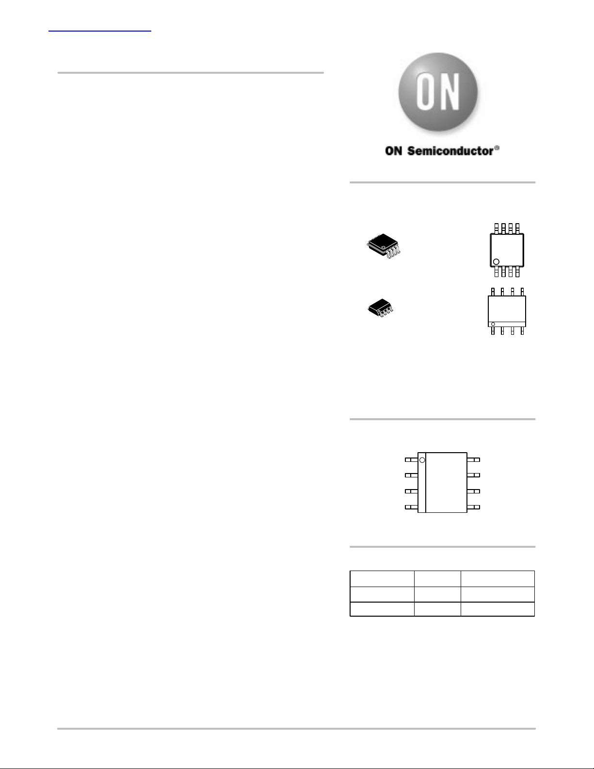
Micro8
DM SUFFIX
CASE 846A
SO−8
D SUFFIX
CASE 751
MARKING
DIAGRAMS
8
1030
AYW
1
8
N1031
ALYW
1
Features
• On Chip High 200 V Power Switch Circuit and Startup Circuit
• Internal Startup Regulator with Auxiliary Winding Override
• Operation up to 1 MHz
• External Frequency Synchronization Capability
• Frequency Fold−down Under Fault Conditions
• Trimmed ± 2% Internal Reference
• Line Undervoltage and Overvoltage Detectors
• Cycle by Cycle Current Limit Using SENSEFET
• Active LEB Circuit
• Overtemperature Protection
• Internal Error Amplifier
T ypical Applications
• Secondary Side Bias Supply for Isolated dc−dc Converters
• Stand Alone Low Power dc−dc Converter
• Low Power Bias Supply
• Low Power Boost Converter
PIN CONNECTIONS
1
GND
2
C
T
3
V
FB
COMP
Device Package Shipping
NCP1030DMR2 Micro8 4000/Tape & Reel
NCP1031DR2 SO−8
†For information on tape and reel specifications,
including part orientation and tape sizes, please
refer to our Tape and Reel Packaging Specification
Brochure, BRD8011/D.
4
(Top View)
ORDERING INFORMATION
8
V
DRAIN
7
V
CC
6
UV
5
OV
†
2500/Tape & Reel
Semiconductor Components Industries, LLC, 2004
August, 2004 − Rev. 4
1 Publication Order Number:
NCP1030/D
Page 2
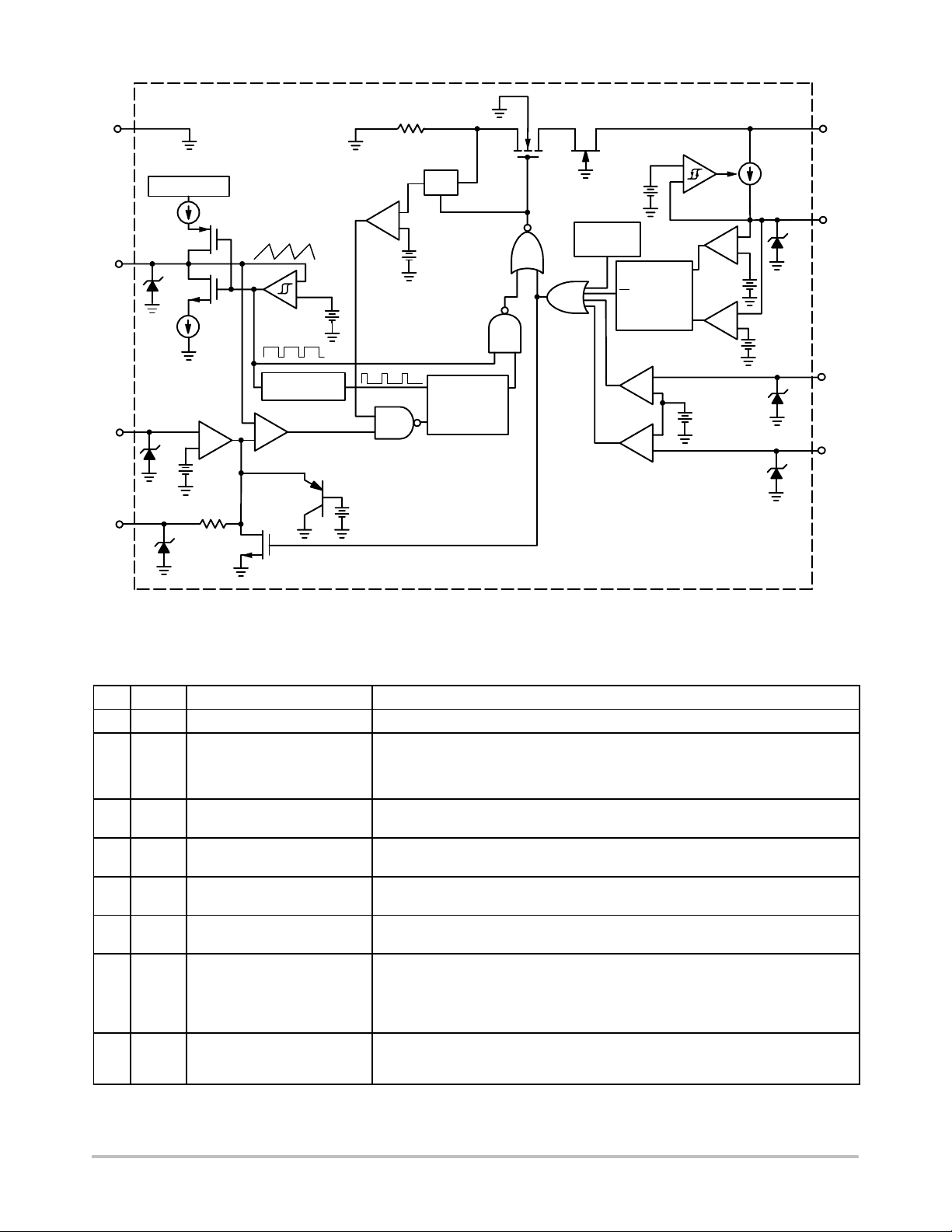
NCP1030, NCP1031
GND
C
VFB
COMP
Internal Bias
T
10 V
Error Amplifier
10 V
10 V
I
I2 = 3I
−
+
+
2.5 V
−
2 k
1
1
Current Limit
Comparator
CT Ramp
+
3.0 V/3.5 V
One Shot
IO
−
Pulse
−
+
PWM Comparator
4.5 V
R
SENSE
LEB
−
+
+
50 mV
−
SQ
Reset
Dominant
Latch
R
PWM Latch
7.5 V/10 V
Thermal
Shutdown
Q
+
−
Reset
Dominant
Latch
−
+
−
+
S
R
Disable
+
2.5 V
−
10 V
+
−
−
+
+
−
+
10 V
10 V
6.5 V
−
I
START
16 V
V
DRAIN
V
CC
UV
OV
Figure 1. NCP1030/31 Functional Block Diagram
FUNCTIONAL PIN DESCRIPTION
Pin Name Function Description
1 GND Ground Ground reference pin for the circuit.
2 C
3 V
T
FB
4 COMP Error Amplifier Compensation Requires external compensation network between COMP and VFB pins. This pin is
5 OV Line Overvoltage Shutdown Line voltage (Vin) is scaled down using an external resistor divider such that the OV
6 UV Line Undervoltage Shutdown Line voltage is scaled down using an external resistor divider such that the UV
7 V
8 V
CC
DRAIN
Oscillator Frequency
Selection
An external capacitor connected to this pin sets the oscillator frequency up to 1 MHz.
The oscillator can be synchronized to a higher frequency by charging or discharging
C
to trip the internal 3.0 V/3.5 V comparator. If a fault condition exists, the power
T
switch is disabled and the frequency is reduced by a factor of 7.
Feedback Input The regulated voltage is scaled down to 2.5 V by means of a resistor divider.
Regulation is achieved by comparing the scaled voltage to an internal 2.5 V reference.
effectively grounded if faults are present.
voltage reaches 2.5 V when line voltage reaches its maximum operating voltage.
voltage reaches 2.5 V when line voltage reaches its minimum operating voltage.
Supply Voltage This pin is connected to an external capacitor for energy storage. During Turn−On, the
startup circuit sources current to charge the capacitor connected to this pin. When the
, the startup circuit turns OFF and the power switch is
CC(on)
should not exceed 16 V.
CC
should not exceed 200 V.
DRAIN
Power Switch and
Startup Circuits
supply voltage reaches V
enabled if no faults are present. An external winding is used to supply power after
initial startup to reduce power dissipation. V
This pin directly connects the Power Switch and Startup Circuits to one of the
transformer windings. The internal High Voltage Power Switch Circuit is connected
between this pin and ground. V
http://onsemi.com
2
Page 3
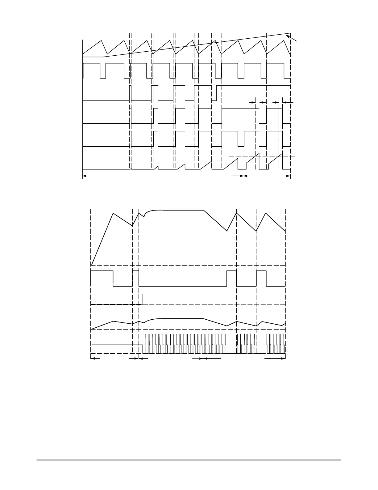
NCP1030, NCP1031
CT Ramp
C
Charge
T
Signal
PWM
Comparator
Output
PWM Latch
Output
Power Switch
Circuit Gate Drive
Leading Edge
Blanking Output
V
COMP Voltage
Current Limit
Propagation Delay
Current Limit
Threshold
Normal PWM Operating Range Output Overload
Figure 2. Pulse Width Modulation Timing Diagram
CC(on)
V
CC(off)
V
CC(reset)
I
START
0 mA
3.0 V
2.5 V
V
DRAIN
0 V
V
UV
0 V
V
FB
0 V
0 V
Power−up &
Normal Operation
Output Overload
standby Operation
Figure 3. Auxiliary Winding Operation with Output Overload Timing Diagram
http://onsemi.com
3
Page 4
NCP1030, NCP1031
MAXIMUM RATINGS
Rating Symbol Value Unit
Power Switch and Startup Circuits Voltage V
Power Switch and Startup Circuits Input Current
− NCP1030
DRAIN
I
DRAIN
− NCP1031
VCC Voltage Range V
All Other Inputs/Outputs Voltage Range V
VCC and All Other Inputs/Outputs Current I
Operating Junction Temperature T
Storage Temperature T
CC
IO
IO
J
stg
Power Dissipation (TJ = 25°C, 2.0 Oz., 1.0 Sq Inch Printed Circuit Copper Clad)
DM Suffix, Plastic Package Case 846A
D Suffix, Plastic Package Case 751
Thermal Resistance, Junction to Air (2.0 Oz. Printed Circuit Copper Clad)
DM Suffix, Plastic Package Case 846A
R
JA
0.36 Sq. Inch
1.0 Sq. Inch
D Suffix, Plastic Package Case 751
0.36 Sq. Inch
1.0 Sq. Inch
Maximum ratings are those values beyond which device damage can occur. Maximum ratings applied to the device are individual stress limit
values (not normal operating conditions) and are not valid simultaneously . If these limits are exceeded, device functional operation is not implied,
damage may occur and reliability may be affected.
A.This device contains ESD protection circuitry and exceeds the following tests:
Pins 1−7: Human Body Model 2000V per MIL−STD−883, Method 3015.
Pins 1−7: Machine Model Method 200 V.
Pin 8 is connected to t he H igh Voltage Startup and Power Switch Circuits a nd rated only to the maximum voltage rating o f t he p art, or 2 00V.
B.This device contains Latchup protection and exceeds 100 mA per JEDEC Standard JESD78.
−0.3 to 200 V
A
1.0
2.0
−0.3 to 16 V
−0.3 to 10 V
100 mA
−40 to 125 °C
−55 to 150 °C
W
0.69
0.93
°C/W
181
162
135
117
http://onsemi.com
4
Page 5
NCP1030, NCP1031
DC ELECTRICAL CHARACTERISTICS (V
V
= 2.5 V, TJ = −40°C to 125°C, typical values shown are for TJ = 25°C unless otherwise noted.) (Note 1)
COMP
Characteristics
= 48 V, VCC = 12 V, CT = 560 pF, VUV = 3 V, VOV = 2 V, VFB = 2.3 V,
DRAIN
Symbol Min Typ Max Unit
STARTUP CONTROL
Startup Circuit Output Current (VFB = V
NCP1030
T
= 25°C
J
T
= −40°C to 125°C
J
V
= 0 V
CC
= V
V
CC
= 0 V
V
CC
V
= V
CC
CC(on)
CC(on)
− 0.2 V
− 0.2 V
COMP
)
I
START
10
6.0
8.0
2.0
12.5
8.6
−
−
15
12
16
13
NCP1031
T
= 25°C
J
T
J
V
= 0 V
CC
V
= V
CC
= −40°C to 125°C
V
= 0 V
CC
= V
V
CC
CC(on)
CC(on)
− 0.2 V
− 0.2 V
13
8.0
11
4.0
16
12
19
16
−
−
21
18
VCC Supply Monitor (VFB = 2.7 V)
Startup Threshold Voltage (V
Minimum Operating V
Hysteresis Voltage
CC
Undervoltage Lockout Threshold Voltage, VCC Decreasing (VFB = V
Minimum Startup Voltage (Pin 8)
I
= 0.5 mA, VCC =V
START
Increasing)
CC
After Turn−on (VCC Increasing)
− 0.2 V
CC(on)
COMP
) V
V
V
CC(on)
V
CC(off)
V
CC(hys)
CC(reset)
START(min)
9.6
7.0
10.2
7.6
−
2.6
10.6
8.0
−
6.0 6.6 7.0 V
− 16.8 18.5
ERROR AMPLIFIER
Reference Voltage (V
TJ = 25°C
T
= −40°C to 125°C
J
Line Regulation (VCC = 8 V to 16 V, TJ = 25°C) REG
Input Bias Current (VFB = 2.3 V) I
COMP Source Current I
COMP Sink Current (VFB = 2.7 V) I
COMP Maximum Voltage (I
COMP Minimum Voltage (I
Open Loop Voltage Gain A
= VFB, Follower Mode)
COMP
= 0 A) V
SRC
= 0 A, VFB = 2.7 V) V
SNK
V
REF
LINE
VFB
SRC
SNK
C(max)
C(min)
VOL
2.45
2.40
2.5
2.5
2.55
2.60
− 1.0 5.0 mV
− 0.1 1.0 A
80 110 140 A
200 550 900 A
4.5 − − V
− − 1.0 V
− 80 − dB
Gain Bandwidth Product GBW − 1.0 − MHz
LINE UNDER/OVERVOLTAGE DETECTOR
Undervoltage Lockout (V
Voltage Threshold (Vin Increasing)
FB
= V
Voltage Hysteresis
Input Bias Current
Overvoltage Lockout (VFB = V
Voltage Threshold (Vin Increasing)
Voltage Hysteresis
Input Bias Current
COMP
COMP
)
V
V
UV(hys)
I
UV
UV
2.400
0.075
−
2.550
0.175
0
2.700
0.275
1.0
)
V
V
OV(hys)
I
OV
OV
2.400
0.075
−
2.550
0.175
0
2.700
0.275
1.0
1. Production testing for NCP1030DMR2 is performed at 25°C only; limits at −40°C and 125°C are guaranteed by design.
mA
V
V
V
V
V
A
V
V
A
http://onsemi.com
5
Page 6
NCP1030, NCP1031
DC ELECTRICAL CHARACTERISTICS (V
V
= 2.5 V, TJ = −40°C to 125°C, typical values shown are for TJ = 25°C unless otherwise noted.) (Note 2)
COMP
Characteristics
= 48 V, VCC = 12 V, CT = 560 pF, VUV = 3 V, VOV = 2 V, VFB = 2.3 V,
DRAIN
Symbol Min Typ Max Unit
OSCILLATOR
Frequency (CT = 560 pF, Note 3)
TJ = 25°C
T
= −40°C to 125°C
J
Frequency (CT = 100 pF) f
Charge Current (VCT = 3.25 V) I
Discharge Current (VCT = 3.25 V) I
f
OSC1
OSC2
CT(C) −
CT(D) −
275
260
300
−
− 800 − kHz
215 − A
645 − A
Oscillator Ramp
Peak
Valley
Vrpk
V
rvly
−
−
3.5
3.0
PWM COMPARATOR
Maximum Duty Cycle
DC
MAX
70 75 80 %
POWER SWITCH CIRCUIT
Power Switch Circuit On−State Resistance (I
NCP1030
T
= 25°C
J
T
= 125°C
NCP1031
J
T
= 25°C
J
= 125°C
T
J
Power Switch Circuit and Startup Circuit Breakdown Voltage
(ID = 100 A, TJ = 25°C)
Power Switch Circuit and Startup Circuit Off−State Leakage Current
(V
= 200 V, VUV = 2.0 V)
DRAIN
T
= 25°C
J
T
= −40 to 125°C
J
= 100 mA)
D
R
DS(on)
V
(BR)DS
I
DS(off)
−
−
−
−
4.1
6.0
2.1
3.5
200 − −
−
−
13
−
Switching Characteristics (VDS = 48 V, RL = 100 )
Rise Time
Fall Time
t
r
t
f
−
−
22
24
CURRENT LIMIT AND OVER TEMPERATURE PROTECTION
Current Limit Threshold (T
NCP1030 (di/dt = 0.5 A/s)
= 25°C)
J
NCP1031 (di/dt = 1.0 A/s)
Propagation Delay, Current Limit Threshold to Power Switch Circuit Output
(Leading Edge Blanking plus Current Limit Delay)
I
t
LIM
PLH
350
700
515
1050
− 100 −
Thermal Protection (Note 4)
Shutdown Threshold (TJ Increasing)
Hysteresis
T
SHDN
T
HYS
125
−
150
45
TOTAL DEVICE
Supply Current After UV Turn−On
Power Switch Enabled
Power Switch Disabled
Non−Fault condition (V
Fault Condition (V
FB
= 2.7 V, V
FB
= 2.7 V)
UV
= 2.0 V)
I
I
I
CC1
CC2
CC3
2.0
−
−
3.0
1.5
0.65
2. Production testing for NCP1030DMR2 is performed at 25°C only; limits at −40°C and 125°C are guaranteed by design.
3. Oscillator frequency can be externally synchronized to the maximum frequency of the device.
4. Guaranteed by design only.
325
kHz
325
V
−
−
7.0
12
3.0
6.0
V
A
25
50
ns
−
−
mA
680
1360
ns
°C
−
−
mA
4.0
2.0
1.2
http://onsemi.com
6
Page 7

NCP1030, NCP1031
TYPICAL CHARACTERISTICS
13.0
12.5
12.0
NCP1030
V
DRAIN
T
= 25°C
J
= 48 V
11.5
11.0
10.5
10.0
9.5
, STARTUP CURRENT (mA)
9.0
START
8.5
I
8.0
0
246810
VCC, SUPPLY VOLTAGE (V)
Figure 4. NCP1030 Startup Current vs. Supply
Voltage
20
18
16
14
12
10
8
6
, STARTUP CURRENT (mA)
4
START
2
I
VCC = V
CC(on)
0
−50 −25 0 25 50 150
TJ, JUNCTION TEMPERATURE (°C)
NCP1030
V
= 48 V
DRAIN
VCC = 0 V
− 0.2 V
75 100 125
20
19
18
NCP1031
V
= 48 V
DRAIN
T
= 25°C
J
17
16
15
14
13
, STARTUP CURRENT (mA)
12
START
11
I
10
0
246810
VCC, SUPPLY VOLTAGE (V)
Figure 5. NCP1031 Startup Current vs. Supply
Voltage
20
18
16
VCC = 0 V
14
12
10
VCC = V
CC(on)
− 0.2 V
8
6
, STARTUP CURRENT (mA)
4
START
2
I
0
−50 −25 0 25 50 150
, JUNCTION TEMPERATURE (°C)
T
J
NCP1031
V
DRAIN
75 100 125
= 48 V
Figure 6. NCP1030 Startup Current vs.
Junction Temperature
12
NCP1030
10
8
TJ = −40°C
TJ = 25°C
6
TJ = 125°C
, STARTUP CURRENT (mA)
2
START
I
0
0425 50 75 100 200
, DRAIN VOLTAGE (V)
V
DRAIN
VCC = V
CC(on)
125 150 175
− 0.2 V
Figure 8. NCP1030 Startup Current vs. Drain
Voltage
20
18
16
14
12
10
8
6
, STARTUP CURRENT (mA)
START
I
2
0
0425 50 75 100 200
http://onsemi.com
7
Figure 7. NCP1031 Startup Current vs.
Junction Temperature
NCP1031
TJ = −40°C
TJ = 25°C
TJ = 125°C
VCC = V
CC(on)
− 0.2 V
125 150 175
, DRAIN VOLTAGE (V)
V
DRAIN
Figure 9. NCP1031 Startup Current vs. Drain
Voltage
Page 8

NCP1030, NCP1031
0
TYPICAL CHARACTERISTICS
11.0
10.5
Startup Threshold
10.0
9.5
9.0
8.5
8.0
7.5
, SUPPLY VOLTAGE (V)
7.0
CC
V
Minimum Operating Threshold
6.5
6.0
−50 −25 0 50 150
T
, JUNCTION TEMPERATURE (°C)
J
75 100 12525
Figure 10. Supply V oltage Thresholds vs.
Junction Temperature
20.0
VCC = V
19.5
19.0
I
START
CC(on)
= 0.5 mA
18.5
18.0
17.5
17.0
16.5
16.0
, MINIMUM STARTUP VOLTAGE (V)
15.5
15.0
−25
−50 0 25 50 75 100 125 150
START(min)
V
TJ, JUNCTION TEMPERATURE (°C)
Figure 12. Minimum Startup Voltage vs.
Junction Temperature
− 0.2 V
6.80
6.75
6.70
6.65
6.60
6.55
6.50
THRESHOLD (V)
6.45
, UNDERVOLTAGE LOCKOUT
6.40
6.35
CC(reset)
6.30
V
−50 −25 0 25 50 15
T
, JUNCTION TEMPERATURE (°C)
J
75 100 125
Figure 11. Undervoltage Lockout Threshold
vs. Junction T emperature
2.70
2.65
2.60
2.55
2.50
2.45
2.40
2.35
, REFERENCE VOLTAGE (V)
2.30
REF
2.25
V
2.20
−25
−50 0 25 50 75 100 125 150
TJ, JUNCTION TEMPERATURE (°C)
Figure 13. Reference V oltage vs. Junction
Temperature
VCC = 12 V
145
140
135
VCC = 12 V
V
= 2.5 V
COMP
V
= 2.3 V
FB
130
125
120
115
110
105
, COMP SOURCE CURRENT (A)
100
SRC
I
95
−50 0 25 50 75 100 125 150
−25
, JUNCTION TEMPERATURE (°C)
T
J
Figure 14. COMP Source Current vs. Junction
Temperature
840
790
740
690
640
590
540
490
, COMP SINK CURRENT (A)
440
SNK
390
I
340
−50 0 25 50 75 100 125 150
http://onsemi.com
8
VCC = 12 V
V
= 2.5 V
COMP
V
= 2.7 V
FB
−25
, JUNCTION TEMPERATURE (°C)
T
J
Figure 15. COMP Sink Current vs. Junction
Temperature
Page 9

NCP1030, NCP1031
TYPICAL CHARACTERISTICS
2.600
2.575
2.550
2.525
2.500
2.475
2.450
2.425
2.400
2.375
2.350
−50 −25 0 50 15075 100 12525
TJ, JUNCTION TEMPERATURE (°C)
, LINE UNDER/OVERVOLTAGE THRESHOLDS (V)
Figure 16. Line Under/Overvoltage Thresholds
UV/OV
V
vs. Junction T emperature
1000
900
800
VCC = 12 V
T
J
700
600
500
400
300
200
, OSCILLATOR FREQUENCY (kHz)
100
OSC
0
f
0 200 400 600 800 1000
CT, TIMING CAPACITOR (pF)
= 25°C
220
210
200
190
180
170
160
, UNDER/OVERVOLTAGE
150
HYSTERESIS (mV)
140
130
UV/OV(hys)
V
120
−25
−50 0 25 50 75 100 125 150
T
, JUNCTION TEMPERATURE (°C)
J
Figure 17. Line Under/Overvoltage Hysteresis
vs. Junction T emperature
1100
1000
900
800
700
600
500
400
300
, OSCILLATOR FREQUENCY (kHz)
200
OSC
f
100
−50 −25 0 25 15050 75 100 125
T
CT = 47 pF
CT = 220 pF
CT = 1000 pF
, JUNCTION TEMPERATURE (°C)
J
VCC = 12 V
Figure 18. Oscillator Frequency vs. Timing
Capacitor
77.0
VCC = 12 V
76.5
76.0
75.5
f
OSC
= 200 kHz
75.0
74.5
74.0
f
= 1000 kHz
OSC
73.5
, MAXIMUM DUTY CYCLE (%)
73.0
MAX
72.5
DC
72.0
−50 −25 0 25 50 75
T
, JUNCTION TEMPERATURE (°C)
J
Figure 20. Maximum Duty Cycle vs. Junction
Temperature
100 125 150
http://onsemi.com
Figure 19. Oscillator Frequency vs. Junction
8
VCC = 12 V
7
I
= 100 mA
D
6
5
4
3
, POWER SWITCH CIRCUIT
2
ON RESISTANCE ()
1
DS(on)
R
0
−50 −25 0 25 50 75
T
, JUNCTION TEMPERATURE (°C)
J
Figure 21. Power Switch Circuit On Resistance
vs. Junction T emperature
9
Temperature
NCP1030
NCP1031
100 125 150
Page 10

NCP1030, NCP1031
TYPICAL CHARACTERISTICS
1000
100
, OUTPUT CAPACITANCE (pF)
OUT
C
10
0 40 80 120 160 200
V
, DRAIN VOLTAGE (V)
DRAIN
NCP1031
NCP1030
Figure 22. Power Switch Circuit Output
Capacitance vs. Drain V oltage
600
575
Current Slew Rate = 500 mA/s
550
525
500
475
450
425
400
375
, CURRENT LIMIT THRESHOLD (mA)
350
LIM
I
−50 −25 0 25 50 75
TJ, JUNCTION TEMPERATURE (°C)
100 125 150
NCP1030
40
VCC = 12 V
35
30
25
20
15
10
5
, POWER SWITCH AND STARTUP
0
CIRCUITS LEAKAGE CURRENT (A)
0 50 100 150
DS(off)
I
V
TJ = −40°C
TJ = 25°C
TJ = 125°C
, DRAIN VOLTAGE (V)
DRAIN
Figure 23. Power Switch Circuit and Startup
Circuit Leakage Current vs. Drain Voltage
1200
1150
Current Slew Rate = 1 A/s
1100
1050
1000
950
900
850
800
750
, CURRENT LIMIT THRESHOLD (mA)
700
LIM
I
−50 −25 0 25 50 75
TJ, JUNCTION TEMPERATURE (°C)
200 250 300
NCP1031
100 125 150
Figure 24. NCP1030 Current Limit Threshold
vs. Junction T emperature
600
575
550
525
500
475
450
425
400
375
, CURRENT LIMIT THRESHOLD (mA)
350
LIM
I
TJ = 25°C
375 400 425 450 475 500
CURRENT SLEW RATE (mA/S)
Figure 26. NCP1030 Current Limit Threshold
vs. Current Slew Rate
NCP1030
http://onsemi.com
10
Figure 25. NCP1031 Current Limit Threshold
vs. Junction T emperature
1200
1150
1100
1050
1000
950
900
850
800
750
, CURRENT LIMIT THRESHOLD (mA)
700
LIM
I
TJ = 25°C
750 800 850 900 950 1000
CURRENT SLEW RATE (mA/S)
Figure 27. NCP1031 Current Limit Threshold
vs. Current Slew Rate
NCP1031
Page 11

NCP1030, NCP1031
TYPICAL CHARACTERISTICS
4.1
V
= 48 V
DRAIN
3.9
T
= 25°C
J
= 560 pF
C
T
3.7
3.5
3.3
3.1
2.9
2.7
, OPERATING SUPPLY CURRENT (mA)
2.5
10 11 12 13 14 15 16
CC1
I
VCC, SUPPLY VOLTAGE (V)
Figure 28. Operating Supply Current vs.
Supply Voltage
10
9
8
7
4.0
3.5
3.0
2.5
2.0
1.5
1.0
, SUPPLY CURRENT (mA)
CC
I
0.5
0
−50 −25 0 25 50 75 100
VUV = 3.0 V, VFB = 2.3 V
VUV = 3.0 V, VFB = 2.7 V
VUV = 2.0 V
TJ, JUNCTION TEMPERATURE (°C)
Figure 29. Supply Current vs. Junction
Temperature
TJ = 25 °C
VCC = 12 V
C
= 560 pF
T
125 150
6
5
3
, POWER SUPPLY CURRENT (mA)
CC
I
2
200 300 400 500 600 700 8004900 1000
f
, OSCILLATOR FREQUENCY (kHz)
OSC
NCP1031
NCP1030
Figure 30. Operating Supply Current vs.
Oscillator Frequency
http://onsemi.com
11
Page 12

NCP1030, NCP1031
+
V
in
−
+
V
out
−
SECONDARY
NCP103x
GND
C
T
V
FB
COMP
V
DRAIN
V
CC
UV
OV
SIDE CONTROL
V
BIAS
GND
Figure 31. Secondary Side Bias Supply Configuration
+
V
in
−
V
CC
NCP103x
V
GND
C
T
V
FB
COMP
DRAIN
V
UV
OV
CC
V
CC
Figure 32. Boost Circuit Configuration
+
V
out
−
http://onsemi.com
12
Page 13

NCP1030, NCP1031
OPERATING DESCRIPTION
Introduction
The NCP1030 and NCP1031 are a family of miniature
monolithic voltage−mode switching regulators designed for
isolated and non−isolated bias supply applications. The
internal startup circuit and the MOSFET are rated at 200 V,
making them ideal for 48 V telecom and 42 V automotive
applications. In addition, the NCP103x family can operate
from an existing 12 V supply. This controller family is
optimized for operation up to 1 MHz.
The NCP103x family incorporates in a single IC all the
active power, control logic and protection circuitry required
to implement, with a minimum of external components,
several switching regulator applications, such as a
secondary side bias supply or a low power dc−dc converter.
The NCP1030 is available in the space saving Micro8
package and is targeted for applications requiring up to 3 W.
The NCP1031 is targeted for applications up to 6 W and is
available in the SO−8 package.
The NCP103x includes an extensive set of features
including over temperature protection, cycle by cycle
current limit, individual line under and overvoltage
detection comparators with hysteresis, and regulator output
undervoltage lockout with hysteresis, providing full
protection during fault conditions. A description of each of
the functional blocks is given below, and the representative
block diagram is shown in Figure 2.
Forward:
V
C
CC
where, I
−1
cos
is the bias current supplied by the VCC capacitor
bias
1
OUTNP
DCVinN
including the IC bias current (I
S
2.6
L
OUTCOUT
CC1
I
bias
) and any additional
(eq. 1)
current used to bias the feedback resistors (if used).
After initial startup, the VCC pin should be biased above
V
using an auxiliary winding. This will prevent the
CC(off)
startup regulator from turning ON and reduce power
dissipation. Also, the load should not be directly connected
to the VCC capacitor. Otherwise, the load may override the
startup circuit. Figure 33 shows the recommended
configuration for a non−isolated flyback converter.
+
Vin
−
NCP103x
GND
CT
VFB
COMP
VDRAIN
VCC
UV
OV
+
V
out
−
Startup Circuit and Undervoltage Lockout
The NCP103x contains an internal 200 V startup regulator
that eliminates the need for external startup components.
The startup regulator consists of a constant current source
that supplies current from the input line (Vin) to the capacitor
on the V
pin (CCC). Once the VCC voltage reaches
CC
approximately 10 V, the startup circuit is disabled and the
Power Switch Circuit is enabled if no faults are present.
During this self−bias mode, power to the NCP103x is
supplied by the VCC capacitor. The startup regulator turns
ON again once V
reaches 7.5 V. This “7.5−10” mode of
CC
operation is known as Dynamic Self Supply (DSS). The
NCP1030 and NCP1031 startup currents are 12 mA and 16
mA, respectively.
If VCC falls below 7.5 V, the device enters a re−start mode.
While in the re−start mode, the V
capacitor is allowed to
CC
discharge to 6.5 V while the Power Switch is enabled. Once
the 6.5 V threshold is reached, the Power Switch Circuit is
disabled and the startup regulator is enabled to charge the
VCC capacitor. The Power Switch is enabled again once the
V
voltage reaches 10 V. Therefore, the external V
CC
CC
capacitor must be sized such that a voltage greater than 7.5
V is maintained on the VCC capacitor while the converter
output reaches regulation. Otherwise, the converter will
enter the re−start mode. Equation (1) provides a guideline
for the selection of the V
capacitor for a forward
CC
converter;
Figure 33. Non−Isolated Bias Supply Configuration
The maximum voltage rating of the startup circuit is
200 V. Power dissipation should be observed to avoid
exceeding the maximum power dissipation of the package.
Error Amplifier
The internal error amplifier (EA) regulates the output
voltage of the bias supply. It compares a scaled output
voltage signal to an internal 2.5 V reference (V
REF
connected to its non−inverting input. The scaled signal is fed
into the feedback pin (
V
) which is the inverting input of the
FB
error amplifier.
The output of the error amplifier is available for frequency
compensation and connection to the PWM comparator
through the COMP pin. T o insure normal operation, the EA
compensation should be selected such that the EA frequency
response crosses 0 dB below 80 kHz.
The error amplifier input bias current is less than 1 A
over the operating range. The output source and sink
currents are typically 110 A and 550 A, respectively.
Under load transient conditions, COMP may need to
move from the bottom to the top of the C
Ramp. A large
T
current is required to complete the COMP swing if small
resistors or large capacitors are used to implement the
compensation network. In which case, the COMP swing will
)
http://onsemi.com
13
Page 14

NCP1030, NCP1031
be limited by the EA sink current, typically 110 A.
Optimum transient response is obtained if the compensation
components allow COMP to swing across its operating
range in 1 cycle.
Line Under and Overvoltage Detector
The NCP103x incorporates individual line undervoltage
(UV) and overvoltage (OV) shutdown circuits. The UV and
OV thresholds are 2.5 V. A fault is present if the UV is below
2.5 V or if the OV voltage is above 2.5 V. The UV/OV
detectors incorporate 175 mV hysteresis to prevent noise
from triggering the shutdown circuits.
The UV/OV circuits can be biased using an external
resistor divider from the input line as shown in Figure 34.
The UV/OV pins should be bypassed using a capacitor to
prevent triggering the UV or OV circuits during normal
switching operation.
V
in
R
1
+
R
2
+
V
OV
−
R
3
V
UV
−
Figure 34. UV/OV Resistor Divider
from the Input Line
The resistor divider must be sized to enable the controller
once V
is within the required operating range. While a UV
in
or OV fault is present, switching is not allowed and the
COMP pin is effectively grounded.
Either of these comparators can be used for a different
function if UV o r O V functions are not needed. For example,
the UV/OV detectors can be used to implement an enable or
disable function. If positive logic is used, the enable signal
is applied to the UV pin while the OV pin is grounded. If
negative logic is used, the disable signal is applied to the OV
pin while biasing the UV pin from V
using a resistor
CC
divider.
Oscillator
The oscillator is optimized for operation up to 1 MHz and
its frequency is set by the external timing capacitor (CT)
connected to the CT pin. The oscillator has two modes of
operation, free running and synchronized (sync). While in
free running mode, an internal current source sequentially
charges and discharges C
generating a voltage ramp
T
between 3.0 V and 3.5 V. Under normal operating
conditions, the charge (I
) and discharge (I
CT(C)
CT(D)
currents are typically 215 A and 645 A, respectively. The
charge:discharge current ratio of 1:3 discharges
CT in 25 %
of the total period. The Power Switch is disabled while C
is discharging, guaranteeing a maximum duty cycle of 75 %
as shown in Figure 35.
CT Ramp
Power Switch
Enabled
Charge
C
T
Signal
75%
Figure 35. Maximum Duty Cycle vs COMP
COMP
Duty Cycle
25 %
Figure 18 shows the relationship between the operating
frequency and CT. If an UV fault is present, both I
I
are reduced by a factor of 7, thus reducing the
CT(D)
operating frequency by the same factor.
The oscillator can be synchronized to a higher frequency
by capacitively coupling a synchronization pulse into the C
pin. In sync mode, the voltage on the C
pin needs to be
T
driven above 3.5 V to trigger the internal comparator and
complete the C
charging period. However, pulsing the C
T
pin before it reaches 3.5 V will reduce the p−p amplitude of
the CT Ramp as shown in Figure 36.
3.0 V/3.5 V
Comparator
Reset
T2 (f2)
Range in Sync
Sync Mode
3.5 V
C
Ramp
3.0 V
T
Free Running
Sync Pulse
T1 (f1) T2 (f2)
Mode
Figure 36. External Frequency Synchronization
Waveforms
The oscillator frequency should be set no more that 25%
below the target sync frequency to maintain an adequate
voltage range and provide good noise immunity. A possible
circuit to synchronize the oscillator is shown in Figure 37.
5 V
C
T
C1
R1
R2
)
Figure 37. External Frequency Synchronization
T
Circuit.
Max
C
C
T
2
Voltage
T
CT(C)
and
T
T
http://onsemi.com
14
Page 15

NCP1030, NCP1031
PWM Comparator and Latch
The Pulse Width Modulator (PWM) Comparator
compares the error amplifier output (COMP) to the C
Ramp and generates a proportional duty cycle. The Power
Switch is enabled while the CT Ramp is below COMP as
shown in Figure 35. Once the CT Ramp reaches COMP, the
Power Switch is disabled. If COMP is at the bottom of the
C
Ramp, the converter operates at minimum duty cycle.
T
While COMP increases, the duty cycle increases, until
COMP reaches the peak of the CT Ramp, at which point the
controller operates at maximum duty cycle.
The CT Charge Signal is filtered through a One Shot Pulse
Generator to set the PWM Latch and enable switching at the
beginning of each period. Switching is allowed while the C
Ramp is below COMP and a current limit fault is not present.
The PWM Latch and Comparator propagation delay is
typically 150 ns. If the system is designed to operate with a
minimum ON time less than 150 ns, the converter will skip
pulses. Skipping pulses is usually not a problem, unless
operating at a frequency close to the audible range. Skipping
pulses is more likely when operating at high frequencies
during high line and minimum load condition.
A series r esistor i s i ncluded f or E SD p rotection b etween t he
EA output a nd t he COMP pin. U nder n ormal o peration, a 2 20
mV offset is observed between the C
Ramp and the COMP
T
crossing points. This is not a problem as the series resistor
does not interact with the error amplifier transfer function.
Current Limit Comparator and Power Switch Circuit
The NCP103x monolithically integrates a 200 V Power
Switch Circuit with control logic circuitry. The Power
Switch Circuit is designed to directly drive the converter
transformer. The characteristics of the Power Switch Circuit
are well known. Therefore, the gate drive is tailored to
control switching transitions and help limit electromagnetic
interference (EMI). The Power Switch Circuit is capable of
switching 200 V.
The Power Switch Circuit incorporates SENSEFET
technology to monitor the drain current. A sense voltage is
generated by driving a sense element, R
, with a current
SENSE
proportional to the drain current. The sense voltage is
compared to an internal reference voltage on the
non−inverting input of the Current Limit Comparator. If the
sense voltage exceeds the reference level, the comparator
resets the PWM Latch and switching is terminated. The
NCP1030 and NCP1031 drain current limit thresholds are
0.5 A and 1.0 A, respectively.
Each time the Power Switch Circuit turns ON, a narrow
voltage spike appears across R
. The spike is due to the
SENSE
Power Switch Circuit gate to source capacitance,
transformer interwinding capacitance, and output rectifier
recovery time. This spike can cause a premature reset of the
PWM Latch. A proprietary active Leading Edge Blanking
(LEB) Circuit masks the current signal to prevent the
T
voltage spike from resetting the PWM Latch. The active
LEB masks the current signal until the Power Switch turn
ON transition is complete. The adaptive LEB period
provides better current limit control compared to a fixed
blanking period.
The current limit propagation delay time is typically
100 ns. This time is measured from when an overcurrent
fault appears at the Power Switch Circuit drain, to the start
of the turn−off transition. Propagation delay must be
factored in the transformer design to avoid transformer
saturation.
T
Thermal Shutdown
Internal Thermal Shutdown circuitry is provided to
protect the integrated circuit in the event the maximum
junction temperature is exceeded. When activated, typically
at 150C, the Power Switch Circuit is disabled. Once the
junction temperature falls below 105C, the NCP103x is
allowed to resume normal operation. This feature is
provided to prevent catastrophic failures from accidental
device overheating. It is not intended to be used as a
substitute for proper heatsinking.
Application Considerations
A 2 W bias supply for a 48 V telecom system was designed
using the NCP1030. The bias supply generates an isolated
12 V output. The circuit schematic is shown in Figure 38.
Application Note AND8119/D describes the design of the
bias supply.
2.2
+
0.033
2.2
NCP1030
GND
CT
VFB
COMP
680p
10k
35−76V
−
0.022
680p
Figure 38. 2 W Isolated Bias Supply Schematic
499
MURA110T3
VDRAIN
VCC
UV
OV
0.01
1M
100 p
45k3
34k
1:2.78
MBRA160T3
0.01
MBRA160T3
2.2
22
12V
4k99
1k30
+
−
10
http://onsemi.com
15
Page 16
SEATING
PLANE
−T−
0.038 (0.0015)
PIN 1 ID
NCP1030, NCP1031
PACKAGE DIMENSIONS
Micro8
DM SUFFIX
CASE 846A−02
ISSUE F
−A−
−
K
G
−B−
8 PL
D
0.08 (0.003) A
M
T
S
B
S
C
H
J
L
NOTES:
1. DIMENSIONING AND TOLERANCING
PER ANSI Y14.5M, 1982.
2. CONTROLLING DIMENSION:
MILLIMETER.
3. DIMENSION A DOES NOT INCLUDE
MOLD FLASH, PROTRUSIONS OR GATE
BURRS. MOLD FLASH, PROTRUSIONS
OR GATE BURRS SHALL NOT EXCEED
0.15 (0.006) PER SIDE.
4. DIMENSION B DOES NOT INCLUDE
INTERLEAD FLASH OR PROTRUSION.
INTERLEAD FLASH OR PROTRUSION
SHALL NOT EXCEED 0.25 (0.010) PER
SIDE.
5. 846A−01 OBSOLETE, NEW STANDARD
846A−02.
DIM MIN MAX MIN MAX
A 2.90 3.10 0.114 0.122
B 2.90 3.10 0.114 0.122
C −−− 1.10 −−− 0.043
D 0.25 0.40 0.010 0.016
G 0.65 BSC 0.026 BSC
H 0.05 0.15 0.002 0.006
J 0.13 0.23 0.005 0.009
K 4.75 5.05 0.187 0.199
L 0.40 0.70 0.016 0.028
INCHESMILLIMETERS
8X
SOLDERING FOOTPRINT
1.04
0.041
3.20
0.126
0.65
6X
0.0256
0.38
0.015
8X
4.24
0.167
SCALE 8:1
5.28
0.208
inches
mm
http://onsemi.com
16
Page 17

−Y−
−Z−
NCP1030, NCP1031
PACKAGE DIMENSIONS
SO−8
D SUFFIX
CASE 751−07
ISSUE AC
−X−
B
H
A
58
1
4
G
D
0.25 (0.010) Z
M
S
Y
SXS
0.25 (0.010)
C
SEATING
PLANE
M
Y
0.10 (0.004)
M
K
N
X 45
M
J
NOTES:
1. DIMENSIONING AND TOLERANCING
PER ANSI Y14.5M, 1982.
2. CONTROLLING DIMENSION:
MILLIMETER.
3. DIMENSION A AND B DO NOT INCLUDE
MOLD PROTRUSION.
4. MAXIMUM MOLD PROTRUSION 0.15
(0.006) PER SIDE.
5. DIMENSION D DOES NOT INCLUDE
DAMBAR PROTRUSION. ALLOWABLE
DAMBAR PROTRUSION SHALL BE 0.127
(0.005) TOTAL IN EXCESS OF THE D
DIMENSION AT MAXIMUM MATERIAL
CONDITION.
6. 751−01 THRU 751−06 ARE OBSOLETE.
NEW STANDARD IS 751−07.
MILLIMETERS
DIMAMIN MAX MIN MAX
4.80 5.00 0.189 0.197
B 3.80 4.00 0.150 0.157
C 1.35 1.75 0.053 0.069
D 0.33 0.51 0.013 0.020
G 1.27 BSC 0.050 BSC
H 0.10 0.25 0.004 0.010
J 0.19 0.25 0.007 0.010
K 0.40 1.27 0.016 0.050
M 0 8 0 8
N 0.25 0.50 0.010 0.020
S 5.80 6.20 0.228 0.244
INCHES
SOLDERING FOOTPRINT
7.0
0.275
0.6
0.024
1.52
0.060
4.0
0.155
1.270
0.050
SCALE 6:1
inches
mm
http://onsemi.com
17
Page 18

NCP1030, NCP1031
Micro8 is a trademark of International Rectifier. SENSEFET is a trademark of Semiconductor Components Industries, LLC.
The products described herein (NCP1030 and NCP1031) may be covered by one or more of the following U.S. patents: 5,418,410; 5,477,175.
There may be other patents pending.
ON Semiconductor and are registered trademarks of Semiconductor Components Industries, LLC (SCILLC). SCILLC reserves the right to make changes without further notice
to any products herein. SCILLC makes no warranty, representation or guarantee regarding the suitability of its products for any particular purpose, nor does SCILLC assume any liability
arising out of the application or use of any product or circuit, and specifically disclaims any and all liability, including without limitation special, consequential or incidental damages.
“Typical” parameters which may be provided in SCILLC data sheets and/or specifications can and do vary in different applications and actual performance may vary over time. All
operating parameters, including “Typicals” must be validated for each customer application by customer’s technical experts. SCILLC does not convey any license under its patent rights
nor the rights of others. SCILLC products are not designed, intended, or authorized for use as components in systems intended for surgical implant into the body, or other applications
intended to support or sustain life, or for any other application in which the failure of the SCILLC product could create a situation where personal injury or death may occur. Should
Buyer purchase or use SCILLC products for any such unintended or unauthorized application, Buyer shall indemnify and hold SCILLC and its officers, employees, subsidiaries, affiliates,
and distributors harmless against all claims, costs, damages, and expenses, and reasonable attorney fees arising out of, directly or indirectly, any claim of personal injury or death
associated with such unintended or unauthorized use, even if such claim alleges that SCILLC was negligent regarding the design or manufacture of the part. SCILLC is an Equal
Opportunity/Affirmative Action Employer. This literature is subject to all applicable copyright laws and is not for resale in any manner.
PUBLICATION ORDERING INFORMATION
LITERATURE FULFILLMENT:
Literature Distribution Center for ON Semiconductor
P.O. Box 61312, Phoenix, Arizona 85082−1312 USA
Phone: 480−829−7710 or 800−344−3860 Toll Free USA/Canada
Fax: 480−829−7709 or 800−344−3867 Toll Free USA/Canada
Email: orderlit@onsemi.com
N. American Technical Support: 800−282−9855 Toll Free
USA/Canada
Japan: ON Semiconductor, Japan Customer Focus Center
2−9−1 Kamimeguro, Meguro−ku, Tokyo, Japan 153−0051
Phone: 81−3−5773−3850
http://onsemi.com
ON Semiconductor Website: http://onsemi.com
Order Literature: http://www.onsemi.com/litorder
For additional information, please contact your
local Sales Representative.
NCP1030/D
18
 Loading...