

Page 1
NCP1027
High-Voltage Switcher
for Medium Power Offline
SMPS Featuring Low
Standby Power
The NCP1027 offers a new solution targeting output power levels
from a few watts up to 15 W in a universal mains flyback application.
Our proprietary high- voltage technology lets us include a power
MOSFET together with a startup current source, all directly
connected to the bulk capacitor. To prevent lethal runaway in low
input voltage conditions, an adjustable brown- out circuitry blocks
the activity until sufficient input level is reached.
Current- mode operation together with an adjustable ramp
compensation offers superior performance in universal mains
applications. Furthermore, an Over Power Protection pin brings the
ability to precisely compensate all internal delays in high input voltage
conditions and optimize the maximum output current capability.
Protection wise, a timer detects an overload or a short- circuit and
stops all operations, ensuring a safe auto- recovery, low duty cycle burst
operation. An integrated, auto- recovery, Overvoltage Protection
permanently monitors the VCC level and temporarily shuts down the
driving pulses in case of an unexpected feedback loop runaway.
Finally, a great R
for standby/auxiliary offline power supplies or applications requiring
higher output power levels.
Features
•Built-in 700 V MOSFET with Typical R
•Current-Mode Fixed Frequency Operation: 65 kHz and 100 kHz
•Fixed Peak Current of 800 mA
•Skip-Cycle Operation at Low Peak Currents
•Internal Current Source for Clean and Lossless Startup Sequence
•Auto-Recovery Output Short Circuit Protection with Timer-Based
Detection
•Auto-Recovery Overvoltage Protection with Auxiliary Winding
Operation
•Programmable Brown-Out Input for Low Input Voltage Detection
•Programmable Over Power Protection
•Input to Permanently Latchoff the Part
•Internal Frequency Jittering for Improved EMI Signature
•Extended Duty Cycle Operation to 80% Typical
•No-Load Input Standby Power of 85 mW @ 265 Vac
•500 mW Loaded, Input Power of 715 mW @ 230 Vac
•These are Pb-Free Devices
figure makes the circuit an excellent choice
DS(on)
of 5.8 W, TJ = 25°C
DS(on)
http://onsemi.com
MARKING
DIAGRAM
8-LEAD PDIP
P SUFFIX
CASE 626A
XXX = 65 or 100
A = Assembly Location
WL = Wafer Lot
YY = Year
WW = Work Week
G = Pb-Free Package
PIN CONNECTIONS
V
CC
Ramp Comp.
Brown-Out
FB
(Top View)
ORDERING INFORMATION
Device Package Shipping*
NCP1027P065G PDIP-8
(Pb-Free)
NCP1027P100G PDIP-8
(Pb-Free)
*For additional information on our Pb-Free strategy
and soldering details, please download the
ON Semiconductor Soldering and Mounting
Techniques Reference Manual, SOLDERRM/D.
P1027PXXX
AWL
YYWWG
GND
OPP
Drain
50 Units / Rail
50 Units / Rail
Typical Applications
•Medium Power AC-DC Adapters for Chargers
•Auxiliary/Standby Power Supplies for ATX and TVS Power Supplies
Reference 230 VAC 90-265 VAC
NCP1027 - 5.8 W 25 W* 15 W*
*Typical values, open-frame, 65 kHz version, R
© Semiconductor Components Industries, LLC, 2007
May, 2007 - Rev. 4
< 75°C/W, TA = 50°C.
q
JA
1 Publication Order Number:
NCP1027/D
Page 2
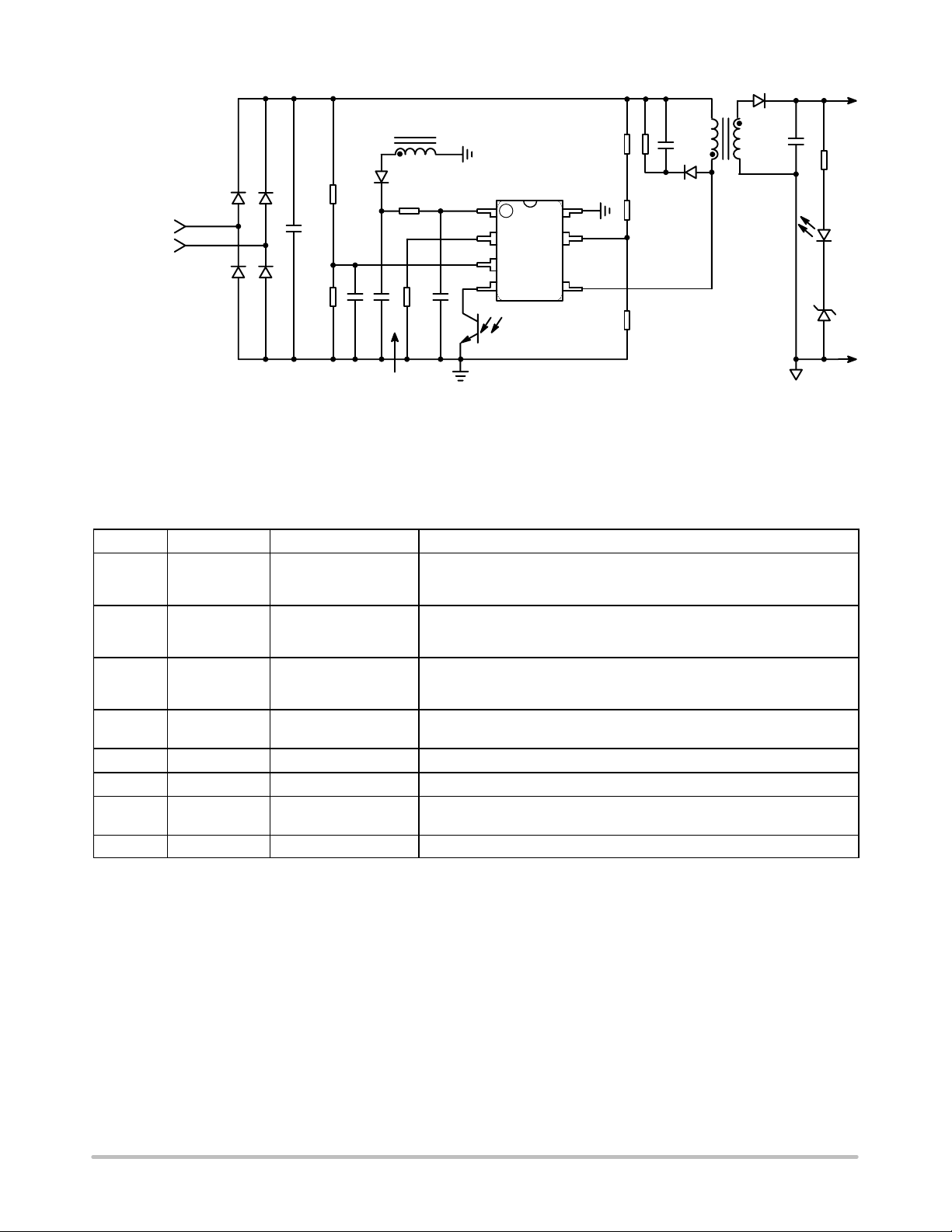
NCP1027
V
out
OPP*
NCP1027
1
2
3
4
8
7
5
85-265 VAC
*Optional component
OVP
+
BO
+
Ramp
Comp.*
+
Figure 1. Typical Application
PIN FUNCTION DESCRIPTION
Pin No. Symbol Function Description
1 V
2 Ramp Comp. Ramp Compensation
3 Brown-Out Brown-Out and
4 FB Feedback Signal Input By connecting an optocoupler to this pin, the peak current setpoint is adjusted
5 Drain Drain Connection The internal drain power switch circuit connection.
- - - This unconnected pin ensures adequate creepage distance.
7 OPP Over Power Protection Driving this pin reduces the power supply capability in high line conditions. If
8 GND The IC Ground -
CC
Powers the Internal
Circuitry
in CCM
Latchoff Input
This pin is connected to an external capacitor of typically 22 mF. The V
includes an active shunt which serves as an auto-recovery overvoltage
protection.
To extend the duty cycle operation in Continuous Conduction Mode (CCM),
pin 3 offers the ability to inject ramp compensation in the controller. If unused,
short this pin to VCC.
By monitoring the bulk level via a resistive network, the circuit protects itself
from low mains conditions. If an external event brings this pin above 4.0 V,
the part fully latches off.
accordingly to the output power demand.
no Over Power Protection is needed, short this pin to ground.
+
GND
CC
http://onsemi.com
2
Page 3
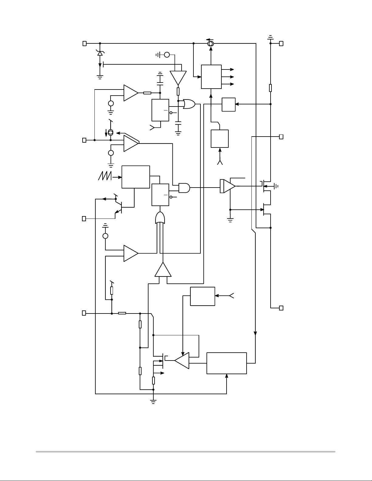
V
BO
CC
Vclamp
Auto-Recovery OVP
+
Vlatch
IBO
+
VBO
20 ms RC
+
-
VCC < 4 V
Reset
+
-
+
S
Q
Q
R
NCP1027
+
-
50 ms RC
IC1
V
CC
Mngt
Fault
Timer
LEB
UVLOs
4 V rst
V
DD
GND
OPP
Ramp
Comp.
FB
Jittering
Icomp
+
V
25%
of lp
V
dd
dd
RFB
65 kHz or
100 kHz
CLOCK
Skip
+
-
Ip Flag
V
cc
S
Q
Q
R
-
+
Soft-Start
UVLO
Drain
+
-
Max Ip Selection
Over Power
Protection Input
Ip Flag
Ramp Compensation
Figure 2. Internal Block Diagram
http://onsemi.com
3
Page 4

NCP1027
MAXIMUM RATINGS
Rating Symbol Value Unit
Power Supply Voltage on all Pins, Except Pin 5 (Drain) V
CC
Drain Voltage BVdss -0.3 to 700 V
Drain Current Peak During Transformer Saturation IDS(pk) 1.8 A
Maximum Current into Pin 1 when Activating the 8.7 V Active Clamp I_V
Thermal Resistance, Junction-to-Air – PDIP7 R
Thermal Resistance, Junction-to-Air – PDIP7 with 1.0 cm@ of 35 m Copper Area R
Maximum Junction Temperature TJ
CC
q
JA
q
JA
MAX
Storage Temperature Range - -60 to +150 °C
ESD Capability, Human Body Model (HBM) (All Pins Except HV) - 2.0 kV
ESD Capability, Machine Model (MM) - 200 V
Stresses exceeding Maximum Ratings may damage the device. Maximum Ratings are stress ratings only. Functional operation above the
Recommended Operating Conditions is not implied. Extended exposure to stresses above the Recommended Operating Conditions may affect
device reliability.
1. This device series contains ESD protection and exceeds the following tests:
Human Body Model 2000 V per Mil-Std-883, Method 3015.
Machine Model Method 200 V.
2. This device contains latchup protection and exceeds 100 mA per JEDEC Standard JESD78.
-0.3 to 10 V
15 mA
100 °C/W
75 °C/W
150 °C
ELECTRICAL CHARACTERISTICS (For typical values T
= 25°C, for min/max values TJ = 0°C to +125°C, Max TJ = 150°C,
J
VCC = 8.0 V, unless otherwise noted.)
Characteristic Pin Symbol Min Typ Max Unit
SUPPLY SECTION AND VCC MANAGEMENT
VCC Increasing Level at which the Switcher Starts to Operate 1 VCC
VCC Decreasing Level at which the Switcher Stops Operation 1 VCC
Hysteresis between VCCON and VCC
(min)
- VCC
Offset Voltage above VCCON at which the Internal Clamp Activates 1 VCC
VCC Voltage at which the Internal Latch is Reset 1 VCC
ON
(min)
hyste
clamp
reset
7.9 8.5 8.9 V
6.7 7.2 7.9 V
- 1.2 - V
140 200 300 mV
- 4.0 - V
Internal IC Consumption, MOSFET Switching at 65 kHz or 100 kHz 1 ICC1 - 1.4 1.9 mA
POWER SWITCH CIRCUIT
Power Switch Circuit On-State Resistance
NCP1027 (Id = 100 mA)
TJ = 25°C
TJ = 125°C
Power Switch Circuit and Startup Breakdown Voltage
(ID
= 120 mA, TJ = 25°C)
(off)
Power Switch and Startup Breakdown Voltage Off-State
5 R
DS(on)
-
-
5.8
9.8
7.0
11
5 BVdss 700 - - V
Idss(OFF)
W
mA
Leakage Current
TJ = 25°C (Vds = 700 V)
TJ = 125°C (Vds = 700 V)
5
5
-
-
50
30
-
-
Switching Characteristics (RL = 50 W, Vds Set for
Idrain = 0.7 x Ilim)
Turn-on Time (90%-10%)
Turn-off Time (10%-90%)
5
5
t
on
t
off
-
-
35
35
-
-
ns
ns
INTERNAL STARTUP CURRENT SOURCE
High-Voltage Current Source, VCC = VCCON – 200 mV 1 IC1 3.5 6.0 8.0 mA
High-Voltage Current Source, VCC = 0 1 IC2 350 650 900 mA
VCC Transition Level for IC1 to IC2 Toggling Point 1 V
CCTh
- 1.3 - V
http://onsemi.com
4
Page 5

NCP1027
ELECTRICAL CHARACTERISTICS (continued) (For typical values T
= 25°C, for min/max values TJ = 0°C to +125°C,
J
Max TJ = 150°C, VCC = 8.0 V, unless otherwise noted.)
Characteristic Pin Symbol Min Typ Max Unit
CURRENT COMPARATOR
Maximum Internal Current Setpoint, Pin 4 Open, TJ = 25°C,
FSW = 65 kHz (Note 3)
Final Switch Current with a Primary Slope of 200 mA/ms,
FSW = 65 kHz (Note 4)
Maximum Internal Current Setpoint, Pin 4 Open, TJ = 25°C,
FSW = 100 kHz (Note 3)
Final Switch Current with a Primary Slope of 200 mA/ms,
FSW = 100 kHz (Note 4)
- Ipeak_27_CS_
65 k
- Ipeak_27_SW_
65 k
- Ipeak_27_CS_
100 k
- Ipeak_27_SW_
100 k
720 800 880 mA
- 820 - mA
720 800 880 mA
- 820 - mA
Setpoint Decrease for a Pin 7 Injected Current of 40 mA, TJ = 25°C 7 IOPP - 23 - %
Voltage Level in Pin 7 at which OPP Starts to Operate 7 IOPPtripV - 1.5 - V
Soft-Start Duration - T
Propagation Delay from Current Detection to Drain OFF State - T
Leading Edge Blanking Duration - T
SS
prop
LEB
- 1.0 - ms
- 100 - ns
- 200 - ns
INTERNAL OSCILLATOR
Oscillation Frequency (Note 5)
65 kHz Version, TJ = 25°C
Oscillation Frequency (Note 5)
100 kHz Version, TJ = 25°C
Frequency Jittering in Percentage of f
OSC
- f
- f
- f
OSC
OSC
Jitter
58.5 65 71.5
90 100 110
- "6.0 - %
Jittering Swing Frequency - fswing - 300 - Hz
Maximum Duty Cycle - Dmax 74 80 87 %
FEEDBACK SECTION
Internal Pullup Resistor 4 Rupp - 16 - kW
Ramp Compensation Level on Pin 1 – Rramp = 100 kW 2 Rlevel - 2.75 - V
SKIP CYCLE GENERATION
Internal Skip Mode Level, in Percentage of Maximum Peak Current - Iskip - 25 - %
PROTECTIONS
Brown-Out Level 3 VBO 510 570 620 mV
Brown-Out Hysteresis Current, TJ = 25°C (Note 3) 3 IBOhyste 10 11.5 13 mA
Brown-Out Hysteresis Current, TJ = 0°C to 125°C 3 IBOhyste - 10 - mA
Fault Validation further to Error Flag Assertion - TimerON 40 55 - ms
OFF Phase in Fault Mode - TimerOFF - 440 - ms
Latching Voltage on Brown-Out Pin 3 Vlatch 3.15 3.5 3.85 V
Latch Input Integrating Filter Time Constant 3 TdelBOL - 20 - ms
OVP Integrating Filter Time Constant - TdelOVP - 50 - ms
VCC Current at which the Switcher Stops Pulsing 1 IOVP 6.0 8.5 11 mA
TEMPERATURE MANAGEMENT
Temperature Shutdown - TSD 160 - - °C
Hysteresis in Shutdown - - - 40 - °C
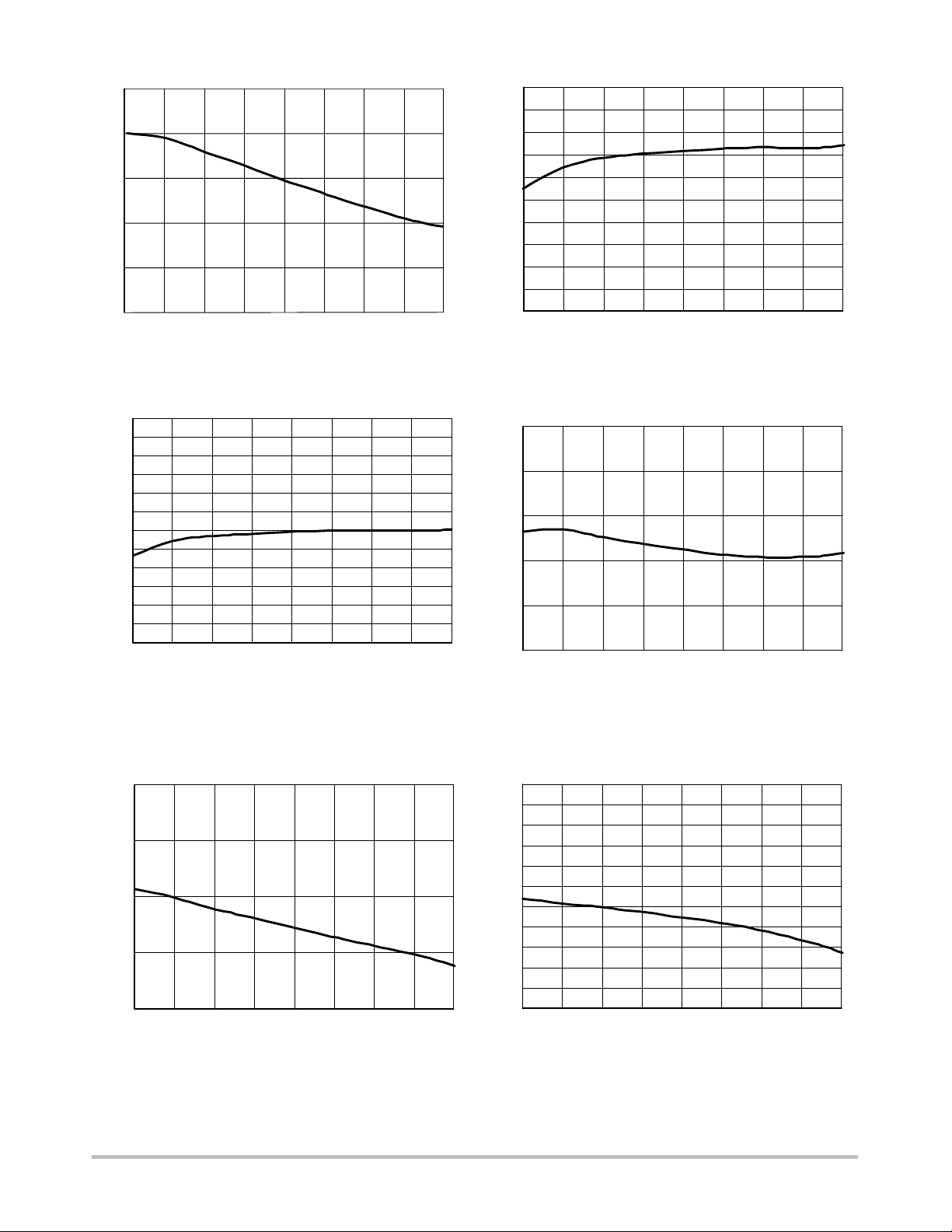
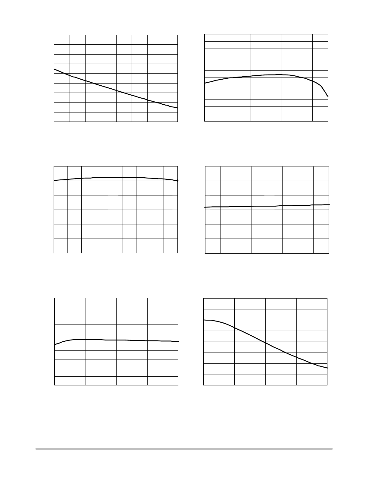
3. See characterization curves for full temperature span evolution.
4. The final switch current is: Ipeak_2X_CS + Tprop x Vin / Lp, with Vin the input voltage and Lp the primary inductor in a flyback.
5. Oscillator frequency is measured with disabled jittering.
kHz
kHz
http://onsemi.com
5
Page 6
NCP1027
(
)
11
10
9
8
IOVP (mA)
7
6
140120100806040200-20
TEMPERATURE (°C)
8.9
8.8
8.7
8.6
8.5
(V)
8.4
CCON
8.3
V
8.2
8.1
8.0
7.9
-20 0 20 40 60 80 100 120 140
TEMPERATURE (°C)
Figure 3. Figure 4.
7.9
7.8
7.7
7.6
7.5
V
7.4
7.3
CCMIN
7.2
V
7.1
7.0
6.9
6.8
6.7
-20 0 20 40 60 80 100 120 140
TEMPERATURE (°C)
(V)
CCClamp
V
0.24
0.22
0.20
0.18
0.16
0.14
140120100806040200-20
TEMPERATURE (°C)
Figure 5. Figure 6.
1.8
1.6
1.4
ICC1 (mA)
1.2
1.0
-20 0 20 40 60 80 100 120 140
TEMPERATURE (°C)
Figure 7. Figure 8.
900
850
800
750
700
650
600
IC2 (mA)
550
500
450
400
350
-20 0 20 40 60 80 100 120 140
http://onsemi.com
6
TEMPERATURE (°C)
Page 7
NCP1027
8.0
7.5
7.0
6.5
6.0
5.5
IC1 (mA)
5.0
4.5
4.0
3.5
-20 0 20 40 60 80 100 120 140
TEMPERATURE (°C)
Figure 9. Figure 10.
120
100
80
60
Fosc (kHz)
40
71.0
70.0
69.0
68.0
67.0
66.0
65.0
64.0
Fosc (kHz)
63.0
62.0
61.0
60.0
59.0
-20 0 20 40 60 80 100 120 140
TEMPERATURE (°C)
87.0
85.0
83.0
81.0
Dmax (%)
79.0
20
0
-40 -20 0 20 40 60 80 100 120 140
TEMPERATURE (°C)
Figure 11. Figure 12.
610
600
590
580
570
560
550
VBO (mV)
540
530
520
510
-20 0 20 40 60 80 100 120 140
TEMPERATURE (°C)
Figure 13.
77.0
75.0
-20 0 20 40 60 80 100 120 140
TEMPERATURE (°C)
13.0
12.5
12.0
11.5
11.0
10.5
10.0
IBO HYSTERESIS (mA)
9.5
9.0
-20 0 20 40 60 80 100 120 140
TEMPERATURE (°C)
Figure 14.
http://onsemi.com
7
Page 8
NCP1027
0
I
k
(
A)
0
0
880
860
840
820
m
800
pea
780
760
740
720
-20 0 20 40 60 80 100 120 140
3.8
3.7
3.6
3.5
Vlatch (V)
3.4
3.3
TEMPERATURE (°C)
Figure 15.
11
10
9
8
7
6
@ ID = 100 mA (W)
5
DS(on)
4
R
3
2
-20 0 20 40 60 80 100 120 14
TEMPERATURE (°C)
Figure 16.
30
28
26
24
22
Iopp (%)
20
18
Ipin 7 = 40 mA
3.2
-20 0 20 40 60 80 100 120 140
TEMPERATURE (°C)
Figure 17.
400
380
360
340
320
300
280
260
Tleb + Tpropdelay (ns)
240
220
200
-20 0 20 40 60 80 100 120 140
TEMPERATURE (°C)
Figure 19.
16
-20 0 20 40 60 80 100 120 14
TEMPERATURE (°C)
Figure 18.
2.8
2.7
2.6
RAMP COMPENSATION LEVEL (V)
2.5
-20 0 20 40 60 80 100 120 14
TEMPERATURE (°C)
Figure 20.
http://onsemi.com
8
Page 9
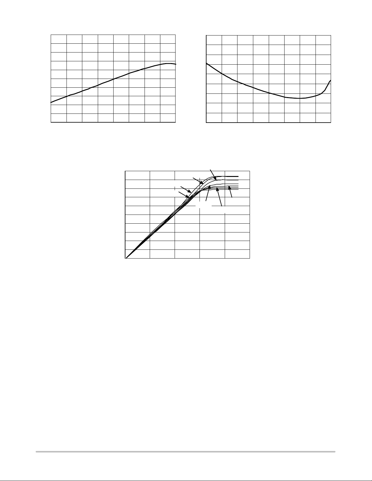
NCP1027
70
68
66
64
62
60
58
TimerON (ms)
56
54
52
50
-20 0 20 40 60 80 100 120 140
TEMPERATURE (°C)
Figure 21.
100%
90%
80%
70%
60%
50%
40%
30%
IPEAK REDUCTION (%)
20%
10%
0%
Figure 23. Ipeak Reduction = F(lopp, @ temperature)
-40 °C
140°C
IOPP (mA)
100
90
80
70
60
50
Idss OFF (mA)
40
30
20
10
-20 0 20 40 60 80 100 120 140
TEMPERATURE (°C)
Figure 22.
85°C
125°C
25°C
0°C
-20 °C
250200150100500
http://onsemi.com
9
Page 10

NCP1027
APPLICATION INFORMATION
Introduction
The NCP1027 offers a complete current-mode control
solution and enhances the NCP101X series. The
component integrates everything needed to build a rugged
and low-cost Switch-Mode Power Supply (SMPS)
featuring low standby power.
• Current-Mode Operation: The controller uses a
current-mode control architecture, which, together
with an adjustable ramp compensation circuitry,
ensures efficient and stable continuous or
discontinuous conduction designs.
• 700 V–5.8 W Power Switch Circuit: Due to
ON Semiconductor Very High Voltage Integrated
Circuit technology, the circuit hosts a high-voltage
power switch circuit featuring a 5.8 W R
25°C. This value lets the designer build a 15 W
power supply operated on universal mains as
long as sufficient copper area exists to lower the
junction-to-ambient thermal resistance. An internal
current source delivers the startup current, necessary
to crank the power supply.
DS(on)
– TJ =
• Short-Cir cuit Protection: By permanently
monitoring the feedback line activity, the circuit is
able to detect the presence of a short-circuit,
immediately reducing the output power for a total
system protection. A 55 ms timer is started as soon as
the feedback pin asks for the maximum peak current.
At the end of this timer, if the fault is still present,
then the device enters a safe, auto-recovery burst
mode, affected by a fixed 440 ms recurrence. Once the
short has disappeared, the controller resumes and goes
back to normal operation. The timer duration is fully
independent from the VCC capacitor value.
• Over Power Protection: A possibility exists to reduce
the maximum output power capability in high line
conditions. A simple two resistor network wired to the
bulk capacitor will program the maximum current
reduction for a given input voltage (down to 20% of
the maximum peak current).
• Fail-Safe Optocoupler/Overvoltage Protection: As
the auxiliary winding is connected to the VCC pin, an
internal active clamp connected between VCC and
ground limits the supply dynamics to 8.7 V. In case
the current injected in this clamp exceeds a level of
6.0 mA (minimum), the controller immediately stops
switching and waits a full timer period before
attempting to restart. If the default is gone, the
controller resumes operation. If the default is still
there, e.g. a broken optocoupler, the controller protects
the load through a safe burst mode.
• Brown-Out Input: A fraction of the input voltage
appears on pin 3, due to a resistive divider. If the
mains drops below a level adjusted by this resistive
divider, the circuit does not switch. As soon as the
mains goes back within its normal range, the device
resumes operation and operates normally. By adjusting
the bridge resistors, it becomes possible to set the
brown-out levels (on and off) independently.
• Latchoff: Pin 3 also welcomes a comparator who
offers a way to fully latch the controller. If an external
event (e.g. an overtemperature) brings the brown-out
pin above 3.5 V, the circuit stays permanently off
until the user cycles its VCC down, for instance by
unplugging the converter from the mains outlet.
• Frequency Jittering: The internal clock receives a
low frequency modulation which helps smoothing the
power supply EMI signature.
• Soft-Start: A 1.0 ms soft-start ensures a smooth
startup sequence, reducing output overshoots.
• Skip Cycle: If SMPS naturally exhibit a good
efficiency at nominal load, they begin to be less
efficient when the output power demand diminishes.
By skipping unneeded switching cycles, the NCP1027
drastically reduces the power wasted during light load
conditions. Experiments carried over the 5.0 V/2.0 A
demonstration board reveal a standby power at
no-load and 265 Vac of 85 mW and an efficiency for
500 mW output power of 64% at 230 Vac.
http://onsemi.com
10
Page 11
NCP1027
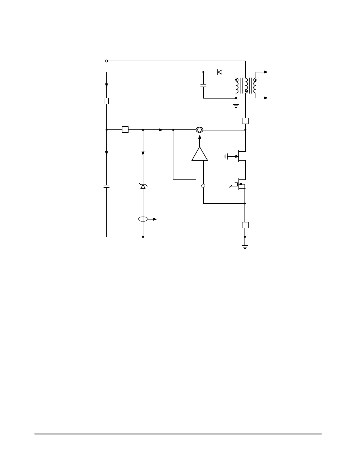
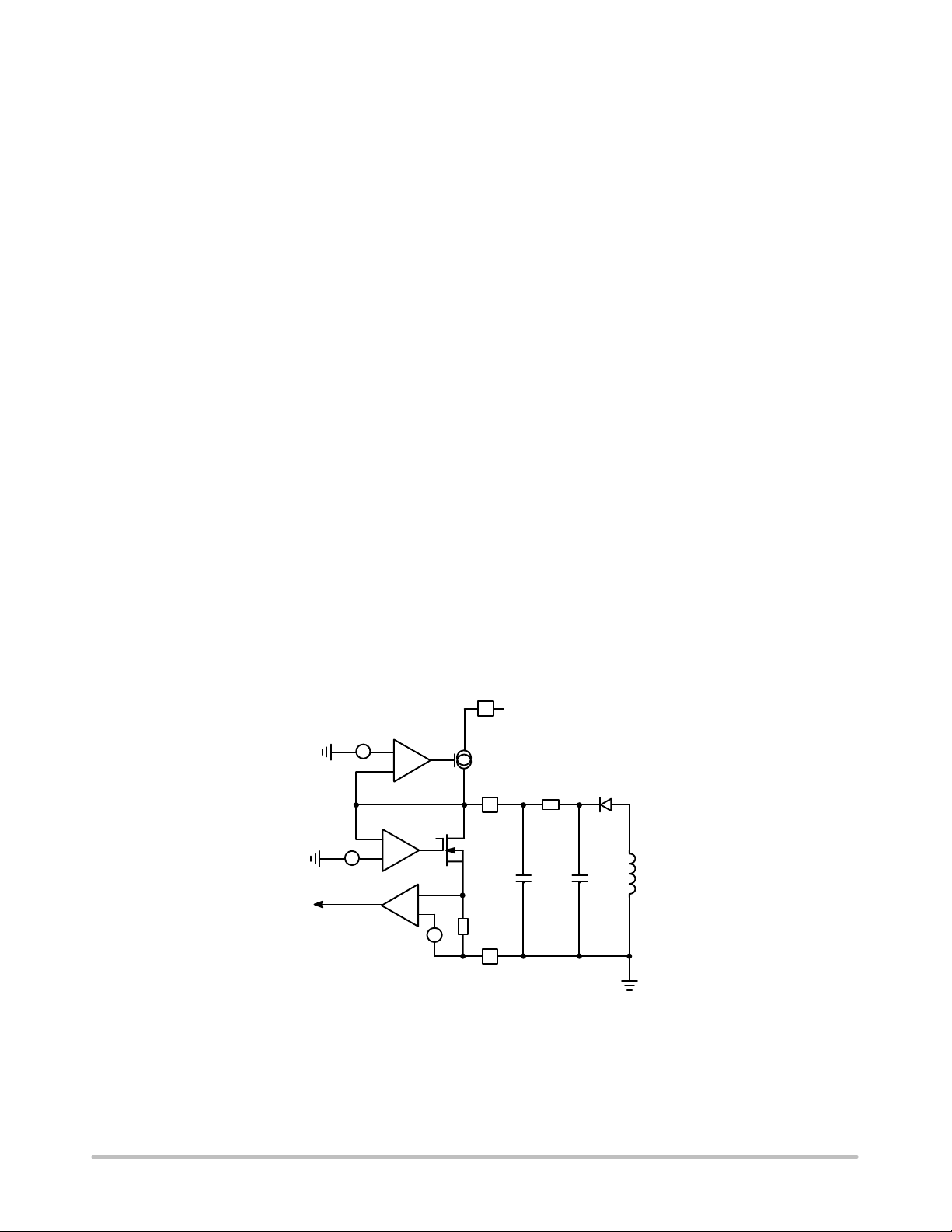
Startup Sequence
The NCP1027 includes a high-voltage startup circuitry,
directly deriving current from the bulk line to charge the
Vbulk
V
capacitor. Figure 24 details the simplified internal
CC
arrangement.
CCon
CCoff
IC1
-
+
←
+
+
5
8
I1
RV
CC
1
I2
+
CV
CC
ICC1
I
clamp
Vz = 8.7 V
I
clamp
→ OVP fault
V
V
> 6 mA
Figure 24. Internal Arrangement of the Startup Circuitry
When the power supply is first connected to the mains
outlet, the internal current source is biased and charges up
the VCC capacitor. When the voltage on this VCC capacitor
reaches the VCCON level (typically 8.5 V), the current
source turns off, reducing the amount of power being
dissipated. At this time, the VCC capacitor only supplies the
controller, and the auxiliary supply should take over before
VCC collapses below VCC
. This VCC capacitor, CVCC,
(min)
must therefore be calculated to hold enough energy so that
VCC stays above VCC
(7.3 V typical) until the
(min)
auxiliary voltage fully takes over.
An auxiliary winding is needed to maintain the VCC in
order to self-supply the switcher. The VCC capacitor has
only a supply role and its value does not impact other
parameters such as fault duration or the frequency sweep
period for instance. As one can see in Figure 24, an internal
active Zener diode, protects the switcher against lethal V
CC
runaways. This situation can occur if the feedback loop
optocoupler fails, for instance, and you would like to
protect the converter against an over voltage event. In that
case, the internal current increase incurred by the V
CC
rapid growth triggers the over voltage protection (OVP)
circuit and immediately stops the output pulses for 440 ms.
Then a new startup attempt takes place to check whether
the fault has disappeared or not. The OVP paragraph gives
more design details on this particular section.
The VCC capacitor can be calculated knowing a) the
amount of energy that needs to be stored; b) the time it
takes for the auxiliary voltage to appear, and; c) the current
consumed by the controller at that time. For a better
understanding, Figure 25 shows how the voltage evolves
on the VCC capacitor upon startup.
http://onsemi.com
11
Page 12

NCP1027
Figure 25. A typical startup sequence showing the VCC capacitor
voltage evolution versus time.
Suppose our power supply takes 10 ms (t
startup
) to bring
the output voltage to its target value. We know that the
switcher consumption is around 2.0 mA (I
). Therefore,
CC1
we can calculate the amount of capacitance we need, to
hold VCC above 7.5 V at least for 10 ms while delivering
2.0 mA:
I
CC1tstartup
C w
C w
DV
2m·10m
1
or, by replacing with the above values,
CC
w 20mF
then select a 33 mF for the V
CC
capacitor.
Fault Condition – Short-Circuit on V
CC
In some fault situations, a short-circuit can purposely
occur between VCC and GND. In high line conditions
(VHV = 370 VDC) the current delivered by the startup
device will seriously increase the junction temperature. For
instance, since IC1 equals 3.0 mA (the min corresponds to
the highest TJ), the device would dissipate 370 3 m =
1.1 W. To avoid this situation, the controller includes a
novel circuitry made of two startup levels, IC1 and IC2. At
powerup, as long as VCC is below a 1.3 V level, the source
delivers IC1 (around 650 mA typical), then, when V
CC
reaches 1.3 V, the source smoothly transitions to IC2 and
delivers its nominal value. As a result, in case of
short-circuit between VCC and GND, the power dissipation
will drop to 370 650 m = 240 mW. Figure 26 portrays
this particular behavior.
Figure 26. The startup source now features a
dual-level startup current.
The first startup period is calculated by the formula
C V = I t, which implies a 33 m 1.3/650 m = 66 ms
startup time for the first sequence (t1). The second
sequence (t2) is obtained by toggling the source to 4.0 mA
with a delta V of VCCON – VCCth = 8.5 – 1.5 = 7.0 V,
which finally leads to a second startup time of
7 33 m/6.0 m = 39 ms. The total startup time becomes
66 m + 39 m = 105 ms as a typical value. Please note that
this calculation is approximated by the presence of the knee
in the vicinity of the transition.
http://onsemi.com
12
Page 13
NCP1027
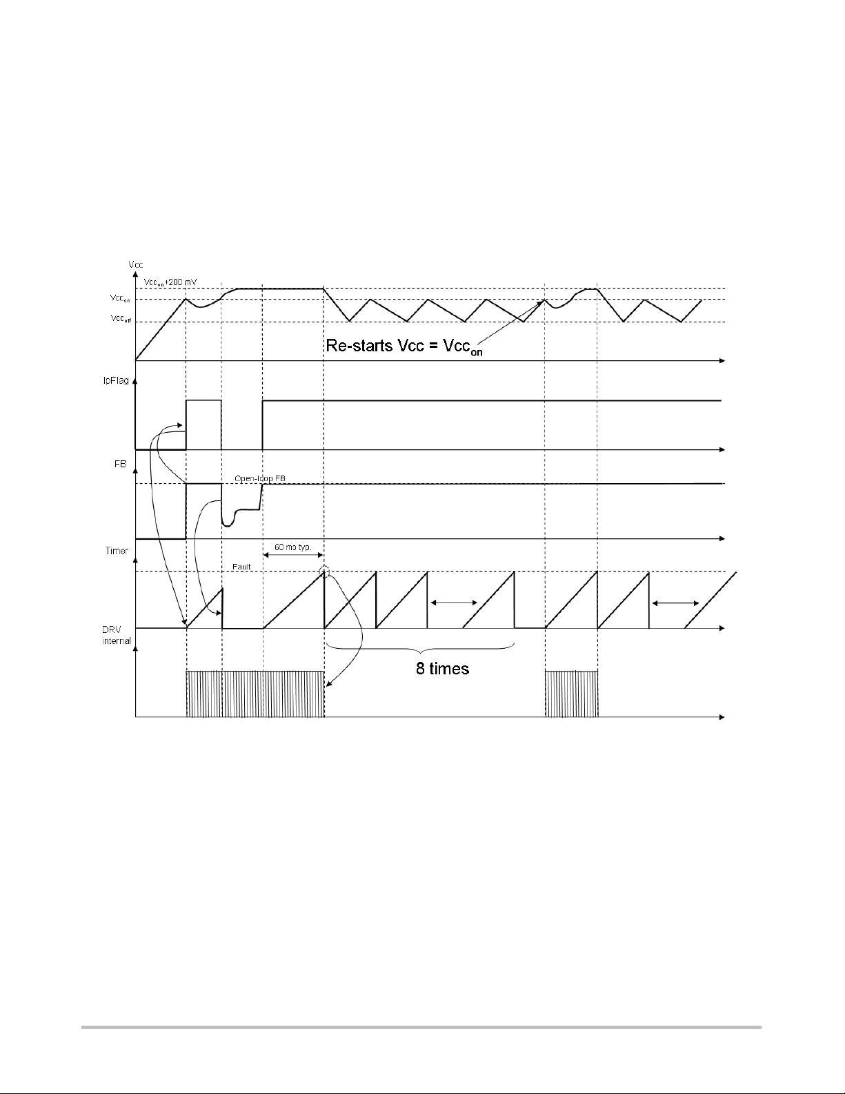
Fault Condition – Output Short-Circuit
As soon as VCC reaches VCCON, drive pulses are
internally enabled. If everything is correct, the auxiliary
winding increases the voltage on the VCC pin as the output
voltage rises. During the start-sequence, the controller
smoothly ramps up the peak current to Imax setting, e.g.
Ipeak_HI, which is reached after a typical period of 1.0 ms.
As soon as the peak current setpoint reaches its maximum
(during the startup period but also anytime an overload
occurs), an internal error flag is asserted, Ipflag, indicating
that the system has reached its maximum current limit set
point (Ip = Ip max). The assertion of this flag triggers a
55 ms counter. If at counter completion Ipflag remains
asserted, all driving pulses are stopped and the part stays off
during eight periods of 55 ms (440 ms). A new attempt to
restart occurs and will last 55 ms providing the fault is still
present. If the fault still affects the output, a safe burst mode
is entered, affected by a low duty-cycle operation (11%).
When the fault disappears, the power supply quickly
resumes operation. Figure 27 depicts this particular mode.
Figure 27. In case of short-circuit or overload, the NCP1027 protects itself and the power supply via a low
frequency burst mode. The V
is maintained by the current source and self-supplies the controller.
CC
http://onsemi.com
13
Page 14

NCP1027
In Figure 27, one can see that the VCC is still alive,
testifying for a badly coupled power secondary and
primary auxiliary windings. Some situations exist where an
output short-circuit make the auxiliary winding collapse
before the timer completion. In this particular case, the
Undervoltage Lock Out (UVLO) circuitry has the priority
and safely cuts off all driving pulses. Figure 28 describes
this variation.
Figure 28. The auxiliary winding collapses in presence of a short-circuit. Pulses are immediately stopped
crosses the minimum operating voltage, VCC
as V
CC
http://onsemi.com
14
(min)
.
Page 15

NCP1027
Fault Condition – Output Too Low
This particular mode of operation occurs when the
feedback is ensured by a two-loop control imposing either
constant output voltage (CV) or constant output current
(CC), for instance in a battery charger. In CC mode, the
output voltage falls down below the original target but the
feedback loop is kept closed by the CC controller. For that
reason, the controller becomes un-able to detect a real
output short-circuit since Ipflag will never be asserted.
Due to a good winding coupling, the primary side auxiliary
collapsing will ensure a proper fault detection via the
UVLO internal circuit. Figure 29 depicts this operating
way.
Figure 29. In this particular case, the output goes low but the timer is not started since the FB pin is still held
by the optocoupler. Due to the UVLO circuit, the controller safely stops operation at V
http://onsemi.com
15
CC
= VCC
(min)
.
Page 16

NCP1027
Fault Condition – Low Input Voltage
The NCP1027 includes a brown-out circuitry able to
protect the power supply in case of low input voltage
conditions. Figure 30 shows how internally the NCP1027
monitors the voltage image of the bulk capacitor. Below a
given level, the controller blocks the driving pulses, above
it, it authorizes them. The internal circuitry, depicted by
1 vin 2 vcmp
160
16.0
Figure 30a, offers a way to observe the high-voltage (HV)
rail. A resistive divider made of R
upper
and R
lower
, brings
a portion of the HV rail on pin 3. Below the turn-on level,
the 10 mA current source IBO is off. Therefore, the turn-on
level solely depends on the division ratio brought by the
resistive divider.
Vbulk = 70 V
IBO
BO
V
DD
ON/OFF
←
+
-
+
VBO
Vbulk
Rupper
Rlower
Figure 30a. The internal brown-out
BO
Plot1
Vcmp Volts
12.0
8.00
4.00
Vbulk = 100 V
120
80.0
Vin in Volts
40.0
0
0
20.0u 60.0u 100u 140u 180u
Time in Seconds
Figure 30b. Simulation results for 100/70 ON/OFF levels.
configuration with an offset current source.
Figure 30.
To the contrary, when the internal BO signal is high, the IBO source is activated and creates an hysteresis. As a result,
it becomes possible to select the turn-on and turn-off levels via a few lines of algebra.
2
1
IBOisOff
R
V()) + V
bulk1
R
lower
lower
) R
upper
IBOisOn
R
lower
R
lower
R
) R
upper
upper
Ǔ
upper
:
We can now extract R
R
V()) + V
from Equation 1 and plug it into Equation 2, then solve for R
lower
bulk2
R
lower
R
upper
R
lower
+ R
+ VBO
lower
) R
lower
) IBO
upper
V
bulk1-Vbulk2
IBO (V
V
bulk1
- VBO
VBO
bulk1
ǒ
- VBO)
If we decide to turn-on our converter for Vbulk1 equals 100 V and turn it off for Vbulk2 equals 70 V, then we obtain:
R
= 3.0 MW
upper
R
= 18 kW
lower
http://onsemi.com
16
(eq. 1)
(eq. 2)
Page 17

NCP1027
The bridge power dissipation is 3302/3.018 Meg =
36 mW in nominal high-line operation. Figure 30b
simulation result confirms our calculations.
Figure 31 describes signal variations during a brown-out
condition. Please note that output pulses only reappear
when VCC reaches V
, ensuring a clean startup
CC(ON)
sequence. As in fault mode conditions, the startup source
is activated on and off and self-supplies the controller in a
Dynamic Self-Supply (DSS) mode.
Figure 31. Signal Evolution During a Brown-Out Condition
Depending on input surge tests, it might be necessary to
wire a filtering capacitor between BO and GND (close to
the circuit) to avoid adversely triggering the internal latch
(unless this is a wanted feature) when the pulse train
appears.
Latchoff Protection
There are some situations where the converter shall be
fully turned-off and stay latched. This can happen in the
presence of a secondary overvoltage (the feedback loop is
drifting) or when an overtemperature is detected.
Secondary monitoring is usually implemented when the
coupling between auxiliary and power windings does not
lead to a precise primary detection, hence the
auto-recovery OVP on pin 1 would not satisfy the precision
requirements. Due to the addition of a comparator on the
BO pin, a simple external circuit can lift up this pin above
VLATCH and permanently disable pulses. The VCC needs
to be cycled down below 3.5 V typically to reset the
controller.
http://onsemi.com
17
Page 18

NCP1027
V
Vout
NTC
CC
Vbulk
Q1
Rupper
BO
Rlower
Figure 32. Adding a comparator on the BO pin offers a way to latch-off the controller.
In Figure 32, Q1 is blocked and does not bother the BO
measurement as long as the NTC and the optocoupler are
not activated. As soon as the secondary optocoupler senses
an OVP condition, or the NTC reacts to a high ambient
20 ms
RC
+
VBO
+
-
+
Vlatch
+
-
IBO
←
To permanent
latch
V
DD
BO
temperature, Q1 base is brought to ground and the BO pin
goes up, permanently latching off the controller. Figure 33
depicts the converter behavior in case of total latch-off.
Figure 33. If the BO pin is lifted up to VLATCH, the controller permanently latches off.
http://onsemi.com
18
Page 19
NCP1027
Auto-Recovery Overvoltage Protection
The particular NCP1027 arrangement offers a simple
way to prevent output voltage runaway when the
optocoupler fails. As Figure 34 shows, an active Zener
diode monitors and protects the VCC pin. Below its
equivalent breakdown voltage, that is to say 8.7 V typical,
no current flows in it. If the auxiliary VCC pushes too much
current inside the Zener, then the controller considers an
OVP situation and stops the pulses. Figure 34 shows that
the insertion of a resistor (R
level and the VCC pin is mandatory a) not to damage the
internal 8.7 V Zener diode during an overshoot for instance
(absolute maximum current is 15 mA) b) to implement the
fail-safe optocoupler protection (OVP) as offered by the
active clamp. Please note that there cannot be bad
interaction between the clamping voltage of the internal
Zener and VCCON since this clamping voltage is actually
built on top of VCCON with a fixed amount of offset
(200 mV typical). R
limit
avoid triggering the OVP as we discussed, but also to avoid
disturbing the VCC in low/light load conditions. The
following details how to evaluate the R
Self-supplying controllers in extremely low standby
applications often puzzles the designer. Actually, if an
SMPS operated at nominal load can deliver an auxiliary
voltage of an arbitrary 16 V (V
below 10 V (V
) when entering standby. This is because
stby
the recurrence of the switching pulses expands so much,
that the low frequency refueling rate of the VCC capacitor
is not enough to keep a proper auxiliary voltage. Figure 35
portrays a typical scope shot of an SMPS entering deep
) between the auxiliary DC
limit
should be carefully selected to
value.
limit
), this voltage can drop
nom
standby (output unloaded). Thus, care must be taken when
calculating R
1) to not trigger the VCC overcurrent latch
limit
(by injecting 6.0 mA into the active clamp – always use the
minimum value for worse case design) in normal operation
but 2) not to drop too much voltage over R
limit
when
entering standby. Otherwise, the converter will enter burst
mode as it will sense an UVLO condition. Based on these
recommendations, we are able to bound R
between two
limit
equations:
V
nom-Vclamp
I
trip
v R
limit
V
stby-VCCON
v
ICC1
(eq. 3)
Where:
V
is the auxiliary voltage at nominal load.
nom
V
is the auxiliary voltage when standby is entered.
stdby
I
is the current corresponding to the nominal operation.
trip
It thus must be selected to avoid false tripping in overshoot
conditions. Always use the minimum of the specification
for a robust design.
ICC1 is the controller consumption. This number slightly
decreases compared to ICC1 from the spec since the part
in standby does almost not switch. It is around 1.0 mA for
the 65 kHz version.
VCC
is the level above which the auxiliary voltage
(min)
must be maintained to keep the controller away from the
UVLO trip point. It is good to obtain around 8.0 V in order
to offer an adequate design margin, e.g. to not reactivate the
startup source (which is not a problem in itself if low
standby power does not matter).
V
= 8.5 V
CCON
V
= 7.5 V
CC(min)
-
+
+
+
-
+
V
= 8.7 V Typ.
Since R
clamp
Latch
Figure 34. A more detailed view of the NCP1027 offers better
insight on how to properly wire an auxiliary winding.
shall not bother the controller in standby, e.g.
limit
+
-
+
keep Vauxiliary to around 8.0 V (as selected above), we
purposely select a Vnom well above this value. As
explained before, experience shows that a 40% decrease
Drain
Startup
←
Source
V
CC
I > 6 mA
Ground
R
limit
+
C
VCC
D1
+
L
AUX
aux
C
can be seen on auxiliary windings from nominal operation
down to standby mode. Let's select a nominal auxiliary
winding of 20 V to offer sufficient margin regarding 8.0 V
when in standby (R
also drops voltage in standby…).
limit
http://onsemi.com
19
Page 20

NCP1027
Plugging the values in Equation 3 gives the limits within
which R
20- 8.7
6m
shall be selected:
limit
v Rlimit v
12- 8
, thatissay : 1.8kW t R
1m
to
t 4kW.
limit
If we design a 65 kHz power supply delivering 12 V, then
the ratio between auxiliary and power must be: 12/20 = 0.6.
The OVP latch will activate when the clamp current
exceeds 6.0 mA. This will occur when Vauxiliary grows up
to:
1. 8.7 + 1.8 k (6 m + 1.8 m) ≈ 23 V for the first
boundary (R
= 1.8 kW).
limit
2. 8.7 + 4 k (6 m + 1.8 m) ≈ 40 V for the second
boundary (R
= 4.0 kW).
limit
Due to a 0.6 ratio between the auxiliary VCC and the
power winding, the auxiliary OVP will be seen as a lower
overshoot on the real output:
1. 23 0.6 ≈ 13.8 V
2. 40 0.6 ≈ 24 V
As one can see, tweaking the R
value will allow the
limit
selection of a given overvoltage output level. Theoretically
predicting the auxiliary drop from nominal to standby is an
almost impossible exercise since many parameters are
involved, including the converter time constants. Fine
tuning of R
thus requires a few iterations and
limit
experiments on a breadboard to check the auxiliary voltage
variations but also the output voltage excursion in fault.
Once properly adjusted, the fail-safe protection will
preclude any lethal voltage runaways in case a problem
would occur in the feedback loop.
> 30 ms
Figure 35. The burst frequency becomes so low
that it is difficult to keep an adequate level on the
auxiliary V
CC
.
Figure 36 describes the main signal variations when the
part operates in auto-recovery OVP.
Figure 36. If the VCC current exceeds a certain threshold, an auto-recovery protection is
activated and protects the design.
http://onsemi.com
20
Page 21

NCP1027
Improving the Precision in Auto-Recovery OVP
Given the OVP variations the internal trip current
dispersion incur, it is sometimes more interesting to
explore a different solution, improving the situation to the
cost of a minimal amount of surrounding elements.
Figure 37 shows that adding a simple Zener diode on top
of the limiting resistor, offers a better precision since what
matters now is the internal 8.7 V VCC breakdown, plus the
Zener voltage. A resistor in series with the Zener diodes
keeps the maximum current in the VCC pin below the
maximum rating of 15 mA just before tripping the OVP.
V
CC
R
limit
+
Ground
Figure 37. A simple Zener diode added in
R
parallel with
, allows for a better
limit
precision OVP.
D1
L
aux
Over Power Compensation
Over Power Compensation or Protection (OPP)
represents a way to limit the effects of the propagation
delay when the converter is supplied from its highest input
voltage. The propagation delay naturally extends the
power capability of any current-limited converter.
Figure 38 explains why. The main parameter is the on
slope, that is to say, the pace at which the inductor current
grows-up when the power switch closes. For a flyback
controller, the slope is given by:
V
Son+
in
L
p
(eq. 4)
where Lp is the transformer magnetizing/primary
inductance and Vin, the input voltage.
As the internal logic takes some time to react, the switch
gate shutdown does not immediately occur when the
maximum power limit is detected (just before activating
the overload protection circuit). Clearly speaking, it can
take up to 100 ns for the NCP1027 current sense
comparator to propagate through the various logical gates
before reaching the power switch and finally shutting it off.
This is the well-known propagation delay noted t
prop
Unfortunately, during this time, the current keeps growing
as Figure 38 depicts. The peak current will therefore be
troubled by this propagation delay. The formula to obtain
the final value is simply:
V
I
peak, final
+
in
L
p
t
prop
) I
peak, max
(eq. 5)
Figure 38. Internal logic blocks take a certain amount
of time before shutting off the driving pulses in
presence of an overcurrent event.
At low line, Son is relatively low and does not bother the
final peak value. The situation differs at high line and
induces a higher peak current. Therefore, the power supply
output power capability increases with the input voltage.
Let us a take a look at a simple example. Suppose the peak
current is 700 mA:
Lp = 1.0 mH
Vin lowline = 100 Vdc
Vin highline = 350 Vdc
I
peak,max
t
prop
= 700 mA
= 100 ns
1
P
out
2
+
I
peak, finalFSWLp
2
h
Where: Fsw is the switching frequency and h the efficiency.
Usually h is bigger in high line conditions than in low line
conditions. This formula is valid for a Discontinuous
Conduction Mode flyback.
From Equation 5, we can calculate the final peak current
in both conditions:
I
peak,final
.
I
peak,final
= (100/1m) x 100n + 700m = 710 mA at low line.
= (350/1m) x 100n + 700m = 735 mA at high line.
From Equation 6, we can have an idea of the maximum
output power capability again, in both conditions with
respective low and high line efficiency numbers of 78%
and 82% for instance:
P
out,lowline
P
out,highline
= 0.5 0.712 1m 65k 0.78 = 12.8 W
= 0.5 0.7352 1m 65k 0.82 = 14.4 W
(eq. 6)
http://onsemi.com
21
Page 22

NCP1027
This difference might not be seen as a problem, but some
design specifications impose stringent conditions on the
maximum output current capability, regardless the line
input. Hence the need for an OPP input…
Since we want to limit the power to 12.8 W at high line,
let us calculate the needed peak current:
2P
From equation 6: I
peak
+
Ǹ
FSWLph
out
= 693 mA to
deliver 12.8 W at high line.
Compared to our 735 mA, we need to decrease the
setpoint by 6% roughly when Vin equals 350 Vdc.
The NCP1027 hosts a special circuitry looking at the
couple voltage/current present on pin 7. Figure 39 shows
how to arrange components around the controller to obtain
Over Power Protection.
Bulk
ROPPU
Current
Setpoint
Figure 39. A resistive network reduces the
power capability in high-line conditions.
Over Power
Protection
OPP
ROPPL
GND
First, you need to know the required injected current and
the voltage across pin 7 to start activating OPP.
Experiments consist in wiring Figure 39 circuit and
running the power supply in conditions where it must shut
down (e.g. highest input voltage and maximum output
current per specification). For this, R
can be put to
OPPL
10 kW and R
made of a series string of 4 1.0 MW
OPPU
resistors plus a 10-turn 1.0 MW potentiometer set at its
maximum value. An amp-meter is inserted in series with
pin 7 and a volt-meter monitors its voltage with respect to
ground. Once the power supply is powered, slowly rotate
the potentiometer and observe both voltage and current
going up at pin 7. At a certain time, as voltage and current
increase, the controller will shut down the power supply.
The current at this time is the one we are looking for.
Suppose these experiments lead to 80 mA with a pin 7
activation voltage of 2.45 V. Final resistor equations are:
VbulkH = 375 Vdc ; the maximum voltage at which OPP
must shut down the controller
V
= 200 Vdc ; the minimum voltage below which
bulkL
OPP is not activated
I
= 80 mA ; the current in pin 7
OPP
Vf = 2.45 V ; the voltage of pin 7 at the above
condition
R
OPPL
R
OPPH
bulkH-VbulkL
+
I
OPP(VbulkL-Vf
+ R
OPPL
V
bulkL-Vf
V
Vf+ 27kW
)
+ 2.2MW
f
(eq. 7)
(eq. 8)
V
If the OPP feature is not needed for some designs, it is
possible to ground it via a copper wire to the adjacent
ground pin. This can help to develop a larger copper area
in an application where the thermal resistance is an
important parameter.
Ramp Compensation
When operating in Continuous Conduction Mode
(CCM), current-mode power supplies can exhibit
so-called sub-harmonic oscillations. To cure this problem,
the designer must inject ramp compensation. The ramp can
either be added to the current sense information or directly
subtracted from the feedback signal. Figure 40 details the
internal arrangement of the ramp compensation circuitry.
V
DD
IRR
Ramp
RR
Figure 40. The Internal Feedback Chain and the Ramp Compensation Network
http://onsemi.com
Gate Reset
Control
Vp
22
Page 23

NCP1027
The principle consists in selecting the RR resistor,
connected from pin 2 to ground, to impose a current IRR in
the transistor collector.
Figure 41. Maximum Peak Current Setpoint
Variations versus Ramp Compensation
The equation to get the right compensation level is the
following:
RR +
Vp2.75k
Sa@T
SW
(eq. 9)
where Vp, the total voltage swing, equals 2.75 V.
Application example:
Suppose we have the following flyback specifications:
Vout = 5.0 V output voltage
Vf = 1.0 V secondary diode forward drop
@ Iout nominal
Np:Ns = 1:N = 1:0.052 transformer turn ratio
Lp = 3.8 mH primary inductance
We can calculate the off slope, the one actually needed
to evaluate Sa, by reflecting the output voltage over the
primary inductance. The slope is projected over a complete
switching period. Here, we use a 65 kHz part.
V
) V
off
+
out
S
NL
p
f
TSW+
6 15u
0.052 3.8m
+ 455mAń15ms
(eq. 10)
Due to the internal sense arrangement, this current slope
will become a voltage slope having a value of:
SȀ
+ 455m 0.375 + 170mVń15ms
off
(eq. 11)
If we chose 50% of this downslope, then the final
compensation ramp will present a slope of:
Sa+
170m
+ 85mVń15ms
2
(eq. 12)
We then have:
RR +
Vp2.75k
Sa@T
SW
2.75 2.75k
+
85m
+ 89kW
(eq. 13)
In the above calculations, the internal ESD resistor has
purposely been omitted to avoid bringing in another
variable. In case no ramp compensation is required, pin 2
must be tied to VCC, the adjacent pin.
Soft-Start
The NCP1027 features a 1.0 ms soft-start, which
reduces the power-on stress, but also contributes to lower
the output overshoot. Figure 42 shows a typical operating
waveform. The NCP1027 features a novel patented
structure which offers a better soft-start ramp, almost
ignoring the startup pedestal inherent to traditional
current-mode supplies.
Figure 42. 1.0 ms Soft-Start Sequence
http://onsemi.com
23
Page 24

NCP1027
Jittering
Frequency jittering is a method used to soften the EMI
signature by spreading the energy in the vicinity of the main
switching component. The NCP1027 offers a "6%
deviation of the nominal switching frequency. The sweep
Jitter ramp
65kHz
61.1kHz
adjustable
Figure 43. Modulation Effects on the Clock Signal by the
Jittering Sawtooth
sawtooth is internally generated and modulates the clock
up and down with a fixed frequency of 300 Hz. Figure 43
shows the relationship between the jitter ramp and the
frequency deviation. It is not possible to externally disable
the jitter.
68.9kHz
Internal
sawtooth
Skip-Cycle
Skip cycle offers an efficient way to reduce the standby
power by skipping unwanted cycles at light loads.
However, the recurrent frequency in skip often enters the
audible range and a high peak current obviously generates
acoustic noise in the transformer. The noise takes its origins
Nominal peak
current
0
in the resonance of the transformer mechanical structure
which is excited by the skipping pulses. A possible
solution, successfully implemented in the NCP1200 series,
also authorizes skip cycle but only when the power demand
as dropped below a given level. This is what Figure 44
shows, as implemented on the NCP1027.
Skip cycle
current limit
Figure 44. Low Peak Current Skip Cycle Guarantees Noise-Free Operation
http://onsemi.com
24
Page 25

NCP1027
5.0 V/3.0 A Universal Mains Power Supply
Due to its low R
, the NCP1027 can be used in
DS(on)
universal mains SMPS up to 15 W of continuous power,
provided that the chip power dissipation is well under
control. That is to say that average power calculations and
measurements have been carried and correlated. The
design of an SMPS around a monolithic device does not
differ from that of a standard circuit using a controller and
a MOSFET. However, one needs to be aware of certain
characteristics specific of monolithic devices. Let us
follow the steps:
350
250
150
50.0
-50.0
> 0 !!
V
min = 120 Vdc
in
V
max = 375 Vdc
in
V
= 5.0 V
out
V
= 15 W
out
Operating mode is CCM
h = 0.8
1. The lateral MOSFET body- diode shall never be
forward biased, either during startup (because of a
large leakage inductance) or in normal operation
as shown by Figure 45. This condition sets the
maximum voltage that can be reflected during t
off
.
1.004M 1.011M 1.018M 1.025M 1.032M
Figure 45. The reflected voltage shall always be greater
than the minimum input voltage to avoid the forward
biasing of the MOSFET body-diode.
As a result, the Flyback voltage which is reflected on the
drain at the switch opening cannot be larger than the input
voltage. When selecting components, you thus must adopt
a turn ratio which adheres to the following equation:
N(V
) Vf) t V
out
in, min
t Vin
min
(eq. 14)
. In our case,
since we operate from a 120 V DC rail while delivering
5.0 V, we can select a reflected voltage of 110 V
DC maximum: 120-110 > 0. Therefore, the turn ratio
V
Np:Ns must be smaller than
Np : Ns t 19. We will see later on how it affects the
in
V
) V
out
110
+
f
5 ) 1
+ 18.3 or
calculation.
2. Lateral MOSFETs have a poorly doped
body-diode which naturally limits their ability to
sustain the avalanche. A traditional RCD
clamping network shall thus be installed to
protect the MOSFET. In some low power
applications, a simple capacitor can also be used
since Vdrain max + V
L
f
peak
Ǹ
C
tot
the total capacitance at the drain
tot
) I
inductance, C
in
(eq. 15)
) N(V
, where L
) Vf)
out
is the leakage
f
node (which is increased by the capacitor you
will wire between drain and source), N the Np:Ns
Figure 46. Primary Inductance Current
Evolution in CCM
turn ratio, V
the output voltage, Vf the
out
secondary diode forward drop and finally, I
the maximum peak current. Worse case occurs
when the SMPS is very close to regulation, e.g.
the V
target is almost reached and I
out
peak
pushed to the maximum. For this design, we have
selected our maximum voltage around 650 V (at
V
= 375 Vdc). This voltage is given by the RCD
in
clamp installed from the drain to the bulk
voltage. We will see how to calculate it later on.
3. Calculate the maximum operating duty-cycle for
this flyback converter operated in CCM:
d
max
+
NV
out
out
) V
in, min
+
1 )
1
V
NV
in,min
out
+ 0.49
NV
4. To obtain the primary inductance, we have the
choice between two equations:
L +
(Vind)
fSWKP
in
(eq. 17)
, where K +
DI
L
I
1
2
defines the amount of ripple we want in CCM
(see Figure 46).
• Small K: deep CCM, implying a large primary
inductance, a low bandwidth and a large leakage
inductance.
peak
is still
(eq. 16)
and
http://onsemi.com
25
Page 26

NCP1027
• Large K: approaching BCM where the rms losses are
the worse, but smaller inductance, leading to a better
leakage inductance.
From Equation 16, a K factor of 0.8 (40% ripple), gives
an inductance of:
(120 0.49)
L +
60k 0.8 18.75
DIL+
Vind
LF
SW
120 0.49
+
3.8m 60k
The peak current can be evaluated to be:
I
avg
DI
I
peak
+
d
)
L
+ I
2
In Figure 46, I1 can also be calculated:
DI
I1+ I
peak
L
-
+ 0.447- 0.129 + 318mA
2
5. Based on the above numbers, we can now
evaluate the conduction losses:
I
d, rms
Ǹ
1 )
+ I1dǸ1 )
1
3
Ǹ
0.258
ǒ
2 0.318
2
+ 3.8mH
+ 258mApeak * to * peak
peak
1
3
2
Ǔ
0.49
DI
2
L
ǒ
Ǔ
2I
1
+ 228mArms
156m
+
DI
L
)
+ 447mA
2
+ 0.318 0.7
If we take the maximum R
for a 120°C junction
DS(on)
temperature, i.e. 11 W, then conduction losses worse case
are:
+ I
2
d, rms
R
ds(on)
+ 571mW
P
cond
6. Off-time and on-time switching losses can be
estimated based on the following calculations:
I
off
+
peakVdstoff
6T
SW
Pon+
+
P
0.447 650 40n
+
I
peak
0.447 114 40n
N(V
out
6T
SW
6 15u
6 15u
) Vf)t
+ 130mW
(eq. 18)
on
(eq. 19)
+ 22mW
The theoretical total power is then 0.571 + 0.13 + 0.022
= 723 mW.
7. The ramp compensation will be calculated as
suggested by Equation 13 giving a resistor of
78 kW or 82 kW for the normalized value.
Power Switch Circuit Protection
As in any Flyback design, it is important to limit the drain
excursion to a safe value, e.g. below the power switch
circuit BVdss which is 700 V. Figures 47a, b, c present
possible implementations:
CV
CC
HV
1
2
3
+
4
8
7
6
5
a. b. c.
Figure 47. Different Options to Clamp the Leakage Spike
HV
R
clamp
CV
CC
+
C
Figure 47a: The simple capacitor limits the voltage
according to Equation 14. This option is only valid for low
power applications, e.g. below 5.0 W, otherwise chances
exist to destroy the MOSFET. After evaluating the leakage
inductance, you can compute C with Equation 15. Typical
values are between 100 pF and up to 470 pF. Large
capacitors increase capacitive losses…
HV
C
clamp
D
1
2
3
4
8
7
6
5
CV
CC
+
Dz
1
2
3
4
Figure 47b: The most standard circuitry called the RCD
network. You calculate R
clamp
and C
clamp
following formulae:
R
clamp
2V
clamp(Vclamp
+
C
clamp
+
L
peak
V
-(V
) Vf)N)
out
2
I
peakFSW
V
clamp
rippleFSWRclamp
D
8
7
6
5
using the
(eq. 20)
(eq. 21)
http://onsemi.com
26
Page 27
NCP1027
is usually selected 50-80 V above the reflected
clamp
value N (V
an MUR160 represents a good choice. One major
drawback of the RCD network lies in its dependency upon
the peak current. Worse case occurs when I
maximum and V
Figure 47c: This option is probably the most expensive
of all three but it offers the best protection degree. If you
need a very precise clamping level, you must implement a
Zener diode or a TVS. There are little technology
differences behind a standard Zener diode and a TVS.
However, the die area is far bigger for a transient suppressor
than that of Zener. A 5.0 W Zener diode, like the 1N5388B,
will accept 180 W peak power if it lasts less than 8.3 ms.
If the peak current in the worse case (e.g. when the PWM
circuit maximum current limit works) multiplied by the
nominal Zener voltage exceeds these 180 W, then the diode
will be destroyed when the supply experiences overloads.
A transient suppressor like the P6KE200 still dissipates
5.0 W of continuous power, but is able to accept surges up
to 600 W @ 1.0 ms. Select the Zener or TVS clamping
level between 40 to 80 V above the reflected output voltage
when the supply is heavily loaded.
+ Vf). The diode needs to be a fast one and
out
and Vin are
peak
is close to reach the steady-state value.
out
Power Dissipation and Heatsinking
The NCP1027 hosting a power switch circuit and a
controller, it is mandatory to properly manage the heat
generated by losses. If no precaution is taken, risks exist to
trigger the internal thermal shutdown (TSD). To help
dissipating the heat, the PCB designer must foresee large
copper areas around the PDI7 package. When surrounded
by a surface greater than 1.0 cm@ of 35 mm copper, it
becomes possible to drop the thermal resistance
junction-to-ambient, R
down to 75°C/W and thus
JA
q
dissipate more power. The maximum power the device can
thus evacuate is: P
max
Tjmax - T
+
R
amb
qJA
max
(eq. 22)
which gives around 930 mW for an ambient of 50°C and a
maximum junction of 120°C. The losses inherent to the
switch circuit R
can be theoretically evaluated, but
DS(on)
the final prototype evaluation must include board
measurements to confirm that the junction temperature
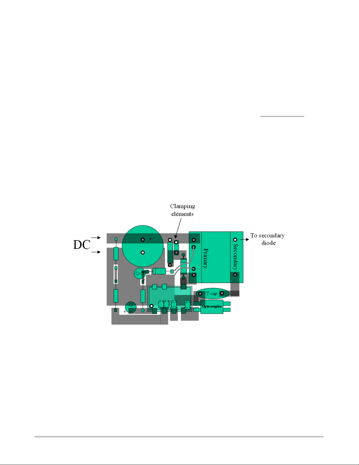
stays within safe limits. Figure 48 gives a possible layout
to help dropping the thermal resistance. When measured on
a 70 mm (2 oz.) copper thickness PCB, we obtained a
thermal resistance of 75°C/W.
Figure 48. A possible PCB arrangement to reduce the thermal resistance
junction-to-ambient.
When routing the printed circuit, it is important to keep
high impedance line very short, like the brown-out signal
and the OPP input if used.
Application Diagram
Figure 49 displays the final application schematic. The
output uses a TLV431 whose low bias current represents an
advantage for low standby power switch mode supplies.
The secondary side features an additional LC filter needed
http://onsemi.com
to remove unwanted spikes, although less problematic than
in DCM operation. On the primary side, a resistive network
senses the input bulk voltage and prevents the controller
from turning on for input voltages below 100 Vdc. The
auxiliary winding delivers 20 V nominal and thus offers
comfortable margin when the converter enters standby. As
we do not use any OPP, pin 7 goes to ground and offers
extended possibility to layout more copper area.
27
Page 28

Vout
3 A
5 V @
R6
10 k
NCP1027
+
C3
100 mF
R7
10 k
L2
2.2 mH
mF
C9
470
mF
C8
470
mF
C5
470
D1
MBRD640CTT4
Np:Ns = 1:0.062
Np:Naux = 1:0.208
Lp = 3.8 mH
C7
R5
+
+
+
10 nF
150 k
R11
1 k
R4
100
Type = 400 V
Type = 1W
D2
1N4637
20 V
D5
C11
+
1N4637
1 mF
R9
U2
NCP1027
5.6 k
C2
100 nF
U1
TL431
C10
2.2 nF
Type = Y1
7
8
1
2
3
45
C12
100 p
R2
78 k
+
10 n
CVCC47 mF
C1
R1
2.8 M
R10
200 k
+
C4
47 mF/
400 V
C13
220 nF
Type = X2
85-265 VAC
R3
Figure 49. 5.0 V-3.0 A Universal Mains Power Supply
http://onsemi.com
28
18 k
Page 29

Transformer Specifications:
Vout = 5.0 V/3.0 A
Vaux = 20 V/10 mA
Lp = 3.8 mH
Ip, rms = 280 mA
Ip, max = 800 mA
Isec, rms = 5.0 A
Fsw = 65 kHz
Np:Nsec = 1 : 0.052
Np:Naux = 1 : 0.208
NCP1027
http://onsemi.com
29
Page 30

NOTE 3
a
-T-
SEATING
PLANE
H
58
B
14
F
A
C
N
D
G
0.13 (0.005) B
NCP1027
PACKAGE DIMENSIONS
8-LEAD PDIP
P SUFFIX
CASE 626A-01
ISSUE O
L
K
M
M
A
T
M
NOTES:
1. DIMENSIONING AND TOLERANCING PER ANSI
Y14.5M, 1982.
2. CONTROLLING DIMENSION: MILLIMETER.
3. PACKAGE CONTOUR OPTIONAL (ROUND OR
SQUARE CORNERS).
4. DIMENSION L TO CENTER OF LEAD WHEN
FORMED PARALLEL.
M
J
5. DIMENSIONS A AND B ARE DATUMS.
DIM MIN MAX MIN MAX
A 9.40 10.16 0.370 0.400
B 6.10 6.60 0.240 0.260
C 3.94 4.45 0.155 0.175
D 0.38 0.51 0.015 0.020
F 1.02 1.78 0.040 0.070
G 2.54 BSC 0.100 BSC
H 0.76 1.27 0.030 0.050
J 0.20 0.30 0.008 0.012
K 2.92 3.43 0.115 0.135
L 7.62 BSC 0.300 BSC
M --- 10 --- 10
N 0.76 1.01 0.030 0.040
INCHESMILLIMETERS
__
The product described herein (NCP1027), may be covered by one or more of the following U.S. patents: 5,418,410; 5,477,175; 6,271,735;
6,362,067; 6,385,060; 6,429,709; 6,448,625; 6,492,679; 6,597,221; 6,633,193; 6,919,598; 6,940,320. There may be other patents pending.
ON Semiconductor and are registered trademarks of Semiconductor Components Industries, LLC (SCILLC). SCILLC reserves the right to make changes without further notice
to any products herein. SCILLC makes no warranty, representation or guarantee regarding the suitability of its products for any particular purpose, nor does SCILLC assume any
liability arising out of the application or use of any product or circuit, and specifically disclaims any and all liability, including without limitation special, consequential or incidental
damages. “Typical” parameters which may be provided in SCILLC data sheets and/or specifications can and do vary in different applications and actual performance may vary over
time. All operating parameters, including “Typicals” must be validated for each customer application by customer's technical experts. SCILLC does not convey any license under
its patent rights nor the rights of others. SCILLC products are not designed, intended, or authorized for use as components in systems intended for surgical implant into the body,
or other applications intended to support or sustain life, or for any other application in which the failure of the SCILLC product could create a situation where personal injury or death
may occur. Should Buyer purchase or use SCILLC products for any such unintended or unauthorized application, Buyer shall indemnify and hold SCILLC and its officers, employees,
subsidiaries, affiliates, and distributors harmless against all claims, costs, damages, and expenses, and reasonable attorney fees arising out of, directly or indirectly, any claim of
personal injury or death associated with such unintended or unauthorized use, even if such claim alleges that SCILLC was negligent regarding the design or manufacture of the part.
SCILLC is an Equal Opportunity/Affirmative Action Employer. This literature is subject to all applicable copyright laws and is not for resale in any manner.
PUBLICATION ORDERING INFORMATION
LITERATURE FULFILLMENT:
Literature Distribution Center for ON Semiconductor
P.O. Box 5163, Denver, Colorado 80217 USA
Phone: 303-675-2175 or 800-344-3860 Toll Free USA/Canada
Fax: 303-675-2176 or 800-344-3867 Toll Free USA/Canada
Email: orderlit@onsemi.com
N. American Technical Support: 800-282-9855 Toll Free
USA/Canada
Europe, Middle East and Africa Technical Support:
Phone: 421 33 790 2910
Japan Customer Focus Center
Phone: 81-3-5773-3850
http://onsemi.com
ON Semiconductor Website: www.onsemi.com
Order Literature: http://www.onsemi.com/orderlit
For additional information, please contact your loc
Sales Representative
NCP1027D
30
 Loading...