

Page 1
NCN5150NGEVB
NCN5150 Evaluation Board
User's Manual
Introduction
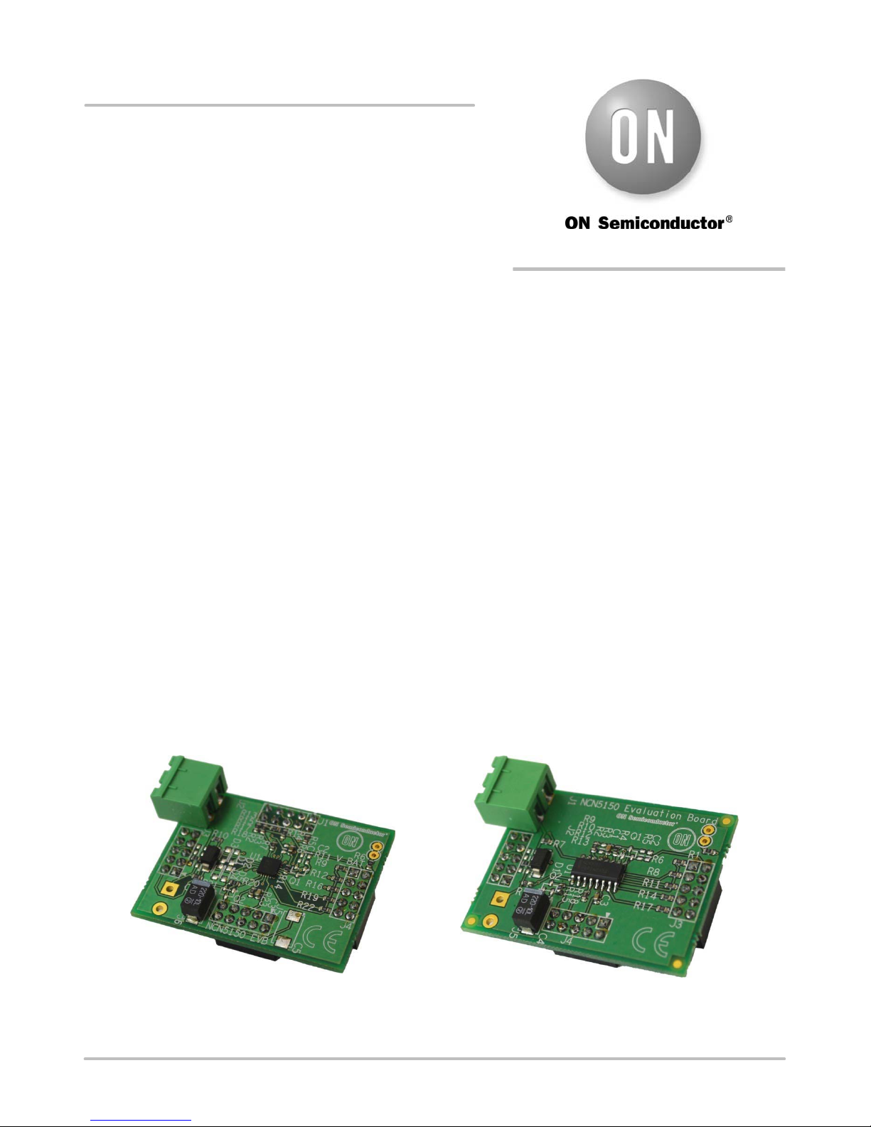
The NCN5150SOICGEVB and NCN5150QFNGEVB
evaluation boards demonstrate the NCN5150 M-BUS
transceiver in SOIC and QFN package respectively. These
evaluation boards include all external components needed
for operating NCN5150 and demonstrate the small PCB
surface area such an implementation requires.
Overview
The NCN5150 is a single-chip integrated slave
transceiver for use in two-wire Meter Bus (M-BUS) slave
devices and repeaters. The transceiver provides all of the
functions needed to satisfy the European Standards EN
13757−2 and EN 1434−3 describing the physical layer
requirements for M-BUS. It includes a programmable
power level of up to 2 (SOIC version) or 6 (NQFP version)
unit loads, which are available for use in external circuits
through a 3.3 V LDO regulator. The NCN5150 can provide
communication up to the maximum M-BUS
communication speed of 38,400 baud (half-duplex).
Applications
Multi-energy Utility Meters
• Water
• Gas
• Electricity
• Heating Systems
Features
• Single-chip MBUS Transceiver
• UART Communication Speeds Up to 38,400 baud
http://onsemi.com
EVAL BOARD USER’S MANUAL
• Integrated 3.3 V VDD LDO Regulator with Extended
Peak Current
• Capability of 15 mA
• Supports Powering Slave Device from the Bus or from
External Power Supply
• Adjustable I/O Levels
• Adjustable Constant Current Sink up to 2 or 6 Unit
Loads Depending on the Package
• Low Bus Voltage Operation
• Extended Current Budget for External Circuits:
minimum 0.8 mA
• Polarity Independent
• Power-Fail Function
• Fast Startup − No External Transistor Required on STC
Pin
• Industrial Ambient Temperature Range of −40°C to
+85°C
• Available in:
♦ 16-pin SOIC (Pin-to-Pin Compatible with
TSS721A)
♦ 20-pin QFN
• These are Pb-free Devices
Figure 1. The NCN5150NGEVB Evaluation Boards
© Semiconductor Components Industries, LLC, 2013
March, 2013 − Rev. 0
1 Publication Order Number:
EVBUM2178/D
Page 2
NCN5150NGEVB
ELECTRICAL CHARACTERISTICS
Table 1. ELECTRICAL CHARACTERISTICS OF THE NCN5150SOICGEVB AND NCN5150QFNGEVB BOARD
Value
Symbol Parameter / Condition
Bus Voltage
V
BUS
Current Drawn from the Bus
I
BUS
Output Voltage
V
DD
Bus Voltage 12 36 42 V
1 UL 1.3 1.5 mA
LDO output 3.1 3.3 3.6 V
NCN5150 DESCRIPTION
Min Typ Max
Unit
The NCN5150 provide a complete transceiver for the
Metering Bus (M-BUS). It consists of a transmit block
which will translate the logic level uart input to current level
signaling on the bus, and a receive block which will translate
the voltage-level signaling on the bus to a logic-level uart
output. The device includes an echo function which will
echo the uart input on the uart output, provided the device is
powered. This can be used by the software stack to monitor
if the message was transmitted. The high voltage level of the
microcontroller interface can be changed by connecting the
desired voltage to the VIO pin. By default, this pin is
NCN5150SOICGEVB DESCRIPTION
General Overview
The NCN5192NGEVB evaluation board demonstrates
the external components required for the operation of the IC.
Loop I/F
NCN5150
connected through a 0R resistor to 3.3 V on the evaluation
boards.
A constant current regulator that will draw a fixed current
from the bus, expressed in unit loads (UL). This current is
made available to the application through a low-dropout
3.3 V regulator. The NCN5150 will detect when the bus is
disconnected and provide an early warning to the
microcontroller that the 3.3 V supply is about to collapse
through the PFb pin.
A thermal shutdown protects the device against high
junction temperatures.
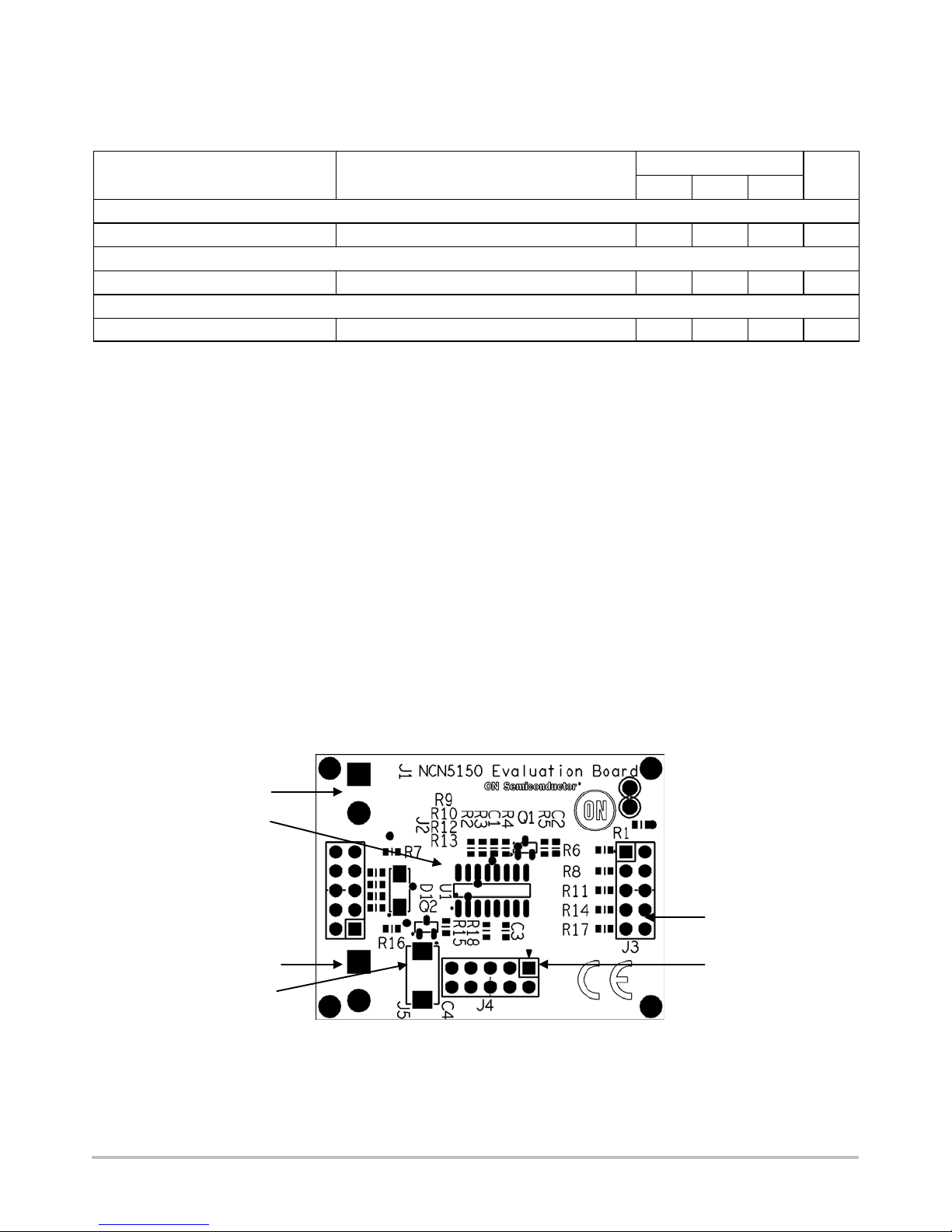
We will cover the different sections below as well as possible
alternatives. A drawing of the board where the different
sections are indicated is shown below.
Loop I/F
STC Capacitor
Figure 2. Board Drawing with Indication of Different Sections
UART I/F
Test I/F
http://onsemi.com
2
Page 3
NCN5150NGEVB
BOM List
Table 2. NCN5150SOICGEVB BILL OF MATERIALS
Quantity Reference Part Footprint Comments Manufacturer Product Code
1 C1 1u C0603 6V3 Multicomp MCCA000515
1 C2 DNP C0603 DNP − −
5 R3, R5, R9, R12,
R13
1 C3 100n C0603 50 V Multicomp MCCA000256
1 C4 220u Case E 10 V AVX TAJD227K010RNJ
1 D1 1SMA40CAT3G SMA ON Semiconductor 1SMA40CAT3G
2 J1,J5 CON2 DNP IMO Precision 21.95MH/2
3 J2,J3,J4 CON10A DNP Multicomp 2214S−10SG−85
2 Q1,Q2 DNP SOT−23 DNP − −
4 R1, R4, R10, R15 0R R0603 62.5 mW Multicomp MC0603WG00000T5E−TR
6 R2, R6, R8, R11,
R14, R17
2 R7, R16 220R R0603 62.5 mW Multicomp MC0.063W06031%220RFR
1 R18 30K R0603 62.5 mW Multicomp MC0.063W06031%30KFR
1 TP1 GND DNP − −
1 TP2 3V3 DNP − −
1 U1 NCN5150 SOIC16 DNP ON Semiconductor NCN5150DR2G
DNP R0603 DNP − −
100R R0603 62.5 mW Multicomp MC0.063W06031%100RFR
http://onsemi.com
3
Page 4
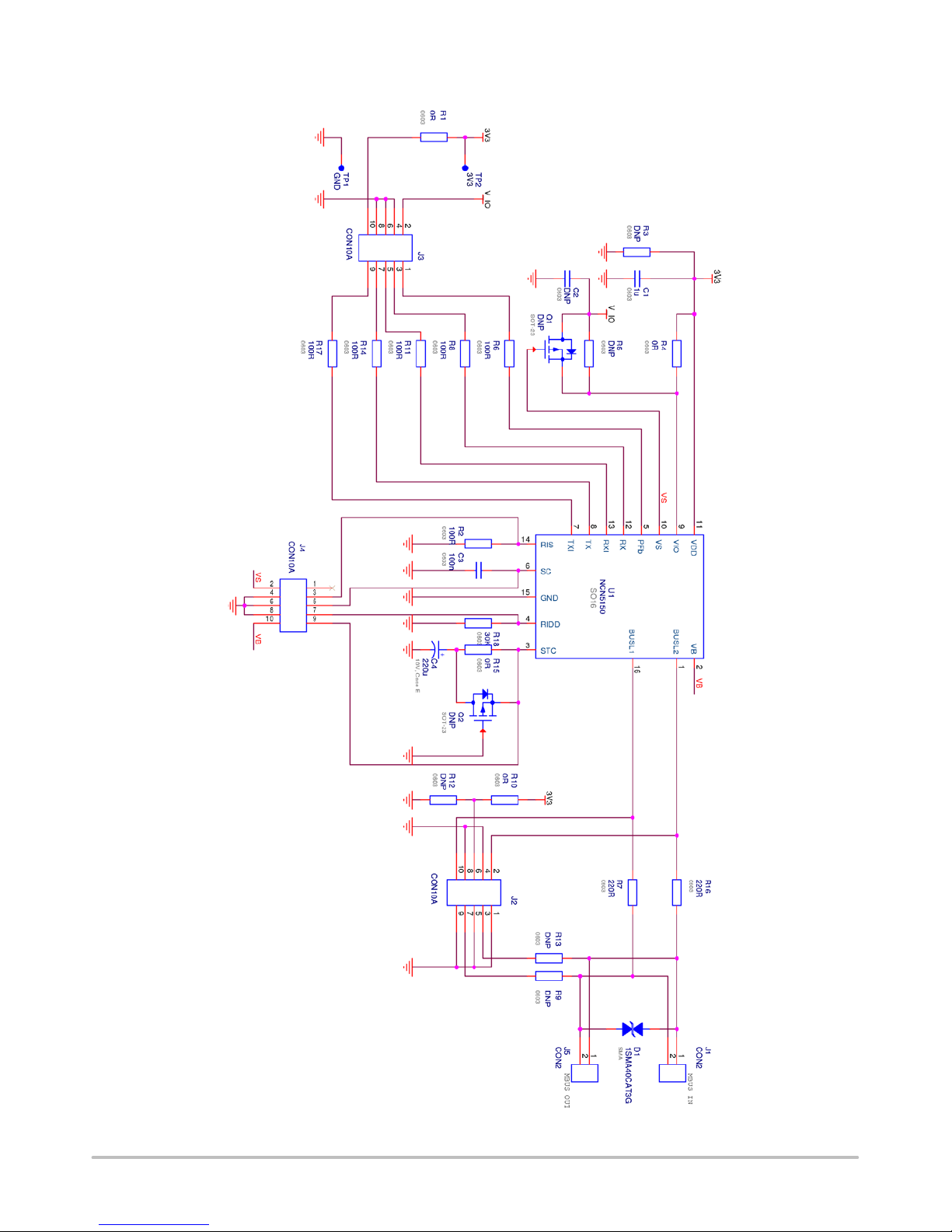
Schematic Diagram
NCN5150NGEVB
Figure 3. Schematic of NCN5150SOICGEVB
http://onsemi.com
4
Page 5

NCN5150NGEVB
NCN5150QFNGEVB DESCRIPTION
General Overview
The NCN5150QFNGEVB evaluation board
demonstrates the external components required for the
below as well as possible alternatives. A drawing of the
board where the different sections are indicated is shown
below.
operation of the IC. We will cover the different sections
Loop I/F
Test I/F
NCN5150
UART I/F
Loop I/F
Test I/F
STC Capacitor
Figure 4. Board Drawing with Indication of Different Sections
BOM List
Table 3. NCN5150QFNGEVB BILL OF MATERIALS
Quantity Reference Part Footprint Comments Manufacturer Product Code
1 C1 1u C0603 6.3 V Multicomp MCCA000515
1 C2 DNP C0603 DNP − −
1 C3 100n C0603 50 V Multicomp MCCA000256
1 C4 220u Case E 10 V AVX TAJD227K010RNJ
1 C5 DNP Case E DNP − −
4 D1, D2, D4, D5 DNP SOD−123 DNP − −
1 D3 1SMA40CAT3G SMA ON Semiconductor 1SMA40CAT3G
4 J1, J3, J4, J5 CON10A DNP IMO Precision 21.95MH/2
2 J2, J6 CON2 DNP Multicomp 2214S−10SG−85
2 Q1, Q2 DNP SOT−23 DNP − −
10 R1,R2,R3,R4,R5,
R8,R11,R13,R15,
R18
6 R7,R9,R12,R16,
R19,R22
4 R6,R14,R17,R20 0R R0603 62.5 mW Multicomp MC0603WG00000T5E−TR
2 R10, R21 220R R0603 62.5 mW Multicomp MC0.063W06031%220RFR
1 R23 30K R0603 62.5 mW Multicomp MC0.063W06031%30KFR
1 TP1 GND DNP − −
1 TP2 3V3 DNP − −
1 U1 NCN5150 QFN20 ON Sample ON Semiconductor NCN5150MNTWG
DNP DNP − −
100R R0603 62.5 mW Multicomp MC0.063W06031%100RFR
http://onsemi.com
5
Page 6

Schematic Diagram
NCN5150NGEVB
Figure 5. Schematic of NCN5150QFNGEVB
http://onsemi.com
6
Page 7

NCN5150NGEVB
FUNCTIONAL DESCRIPTION
Power Supply
The NCN5150 provides power to be used in the
application. To do this, the NCN5150 draws a fixed current
from the bus. The amount of current drawn is fixed at a
number of unit loads (intervals of 1.5 mA) and can be set by
changing the value of the RIDD resistor. The SOIC version
can support up to 2 UL, while the QFN version can support
up to 6 UL. The required resistors for are shown in table xx.
Also shown in table xx is the maximum amount of
capacitance allowed on the STC pin. This limit will ensure
that the transceiver will start up in less than 3 s as required
by the M-BUS standard. Using a smaller capacitor on STC
is allowed, and will result in faster start-up, but also in a
faster shutdown, reducing the time between the early
warning PFb toggling (when the bus is removed) and the
point where the 3.3V VDD voltage can no longer be
maintained. The minimum allowed capacitance on STC is
10 times the capacitance on the VDD pin. The minimum
required capacitance on the VDD pin is 1 mF.
Table 4. UL, RIDD VALUES, STC CAPACITANCE
Number of
Unit Loads
1
2
3
4
5
6
RIDD
Value
30 kW 330 mF
13 kW 820 mF
8.45 kW 1200 mF
6.19 kW 1500 mF
4.87 kW 2200 mF
4.02 kW 2700 mF
Maximum STC
Capacitor Value
Min. Avail-
able Current
0.88 mA
2.10 mA
3.10 mA
4.20 mA
5.30 mA
6.50 mA
Shown in Figure 6 is the startup sequence of the device.
Note that the NCN5150 does not require any external
(PMOS) transistor on the STC pin for proper startup. The
yellow waveform is the bus voltage, the purple waveform
the STC voltage, the green waveform the VDD output, and
the blue waveform the TX output.
Shown in Figure 7 is the shutdown sequence of the device.
The green waveform is the bus voltage, the blue waveform
Figure 6. NCN5150 Startup Sequence
is the VDD output, the purple waveform is the PFb output,
and the yellow waveform is the TX output.
http://onsemi.com
7
Page 8

NCN5150NGEVB
Figure 7. NCN5150 Shutdown Sequence
UART Interface IDC1
The interface between the transceiver and an external
microcontroller is a standard uart interface consisting of the
TX and RX. Alternatively, inverted signals, TXI and RXI,
which are active high, are also available. Only one signal
from TX and TXI, or from RX and RXI can be used at the
same time. The uart pins can handle communication up to
38400 baud. The M-BUS standard requires communication
with 1 start bit, 8 data-bits, 1 even parity bit and 1 stop bit.
Also available on the same connector is the VIO
connection, PFb indication and 3V3 VDD output.
Table 5. MICROCONTROLLER INTERFACE
Pin
number
Signal Type Description
1 PFb Output Bus failure indication
2 VIO Power IO voltage level
3 RX Input UART input
5 RXI Input UART input, inverted
7 TX Output UART output
9 TXI Output UART output, Inverted
4, 6, 8 GND Power Ground
10 VDD Power 3V3 Output
Transmitter
The M-Bus transmitter translated the RX or RXI voltage
levels to current levels on the bus. Typically, 15 mA is added
when transmitting a space.
V
RX
V
RXI
I
BUS
V
IO
V
IO
I
= I
SPACE
= N unit loads
I
MARK
MARK
t
t
+ 15 mA
t
Figure 8. Output Waveforms
Receiver
The receiver will compare the bus voltage level with the
mark level stored on the SC capacitor minus the threshold
level (typically 6 V). It will translate these voltage levels to
low voltage communication on the TX and TXI pins. The
high voltage of these pins is determined by the VIO voltage.
V
BUS
V
TX
V
TXI
V
MARK
VT = V
V
SPACE
V
IO
V
IO
= [21V, 42V]
– 6V
MARK
= V
− 12V
MARK
t
t
t
Figure 9. Receive Waveforms
http://onsemi.com
8
Page 9

Evaluation Board Layout
NCN5150NGEVB
APPENDIX
Figure 10. Top Layer Layout (SOIC)
Figure 11. Bottom Layer Layout (SOIC)
http://onsemi.com
9
Page 10

NCN5150NGEVB
Figure 12. Top Layer Layout (QFN)
Figure 13. Bottom Layer Layout (QFN)
http://onsemi.com
10
Page 11

NCN5150NGEVB
ON Semiconductor and are registered trademarks of Semiconductor Components Industries, LLC (SCILLC). SCILLC owns the rights to a number of patents, trademarks,
copyrights, trade secrets, and other intellectual property. A listing of SCILLC’s product/patent coverage may be accessed at www.onsemi.com/site/pdf/Patent−Marking.pdf. SCILLC
reserves the right to make changes without further notice to any products herein. SCILLC makes no warranty, representation or guarantee regarding the suitability of its products for any
particular purpose, nor does SCILLC assume any liability arising out of the application or use of any product or circuit, and specifically disclaims any and all liability, including without
limitation special, consequential or incidental damages. “Typical” parameters which may be provided in SCILLC data sheets and/or specifications can and do vary in different applications
and actual performance may vary over time. All operating parameters, including “Typicals” must be validated for each customer application by customer’s technical experts. SCILLC
does not convey any license under its patent rights nor the rights of others. SCILLC products are not designed, intended, or authorized for use as components in systems intended for
surgical implant into the body, or other applications intended to support or sustain life, or for any other application in which the failure of the SCILLC product could create a situation where
personal injury or death may occur. Should Buyer purchase or use SCILLC products for any such unintended or unauthorized application, Buyer shall indemnify and hold SCILLC and
its officers, employees, subsidiaries, affiliates, and distributors harmless against all claims, costs, damages, and expenses, and reasonable attorney fees arising out of, directly or indirectly,
any claim of personal injury or death associated with such unintended or unauthorized use, even if such claim alleges that SCILLC was negligent regarding the design or manufacture
of the part. SCILLC is an Equal Opportunity/Affirmative Action Employer. This literature is subject to all applicable copyright laws and is not for resale in any manner.
PUBLICATION ORDERING INFORMATION
LITERATURE FULFILLMENT:
Literature Distribution Center for ON Semiconductor
P.O. Box 5163, Denver, Colorado 80217 USA
Phone: 303−675−2175 or 800−344−3860 Toll Free USA/Canada
Fax: 303−675−2176 or 800−344−3867 Toll Free USA/Canada
Email: orderlit@onsemi.com
N. American Technical Support: 800−282−9855 Toll Free
USA/Canada
Europe, Middle East and Africa Technical Support:
Phone: 421 33 790 2910
Japan Customer Focus Center
Phone: 81−3−5817−1050
http://onsemi.com
11
ON Semiconductor Website: www.onsemi.com
Order Literature: http://www.onsemi.com/orderlit
For additional information, please contact your local
Sales Representative
EVBUM2178/D
Page 12

Mouser Electronics
Authorized Distributor
Click to View Pricing, Inventory, Delivery & Lifecycle Information:
ON Semiconductor:
NCN5150SOICGEVB
 Loading...