

Page 1
NCN4555
1.8V / 3V SIM Card Power
Supply and Level Shifter
The NCN4555 is a level shifter analog circuit designed to translate
the voltages between a SIM Card and an external microcontroller or
MPU. A built−in LDO−type DC−DC converter makes the NCN4555
useable to drive 1.8 V and 3.0 V SIM card. The device fulfills the
ISO7816−3 smart card interface standard as well as GSM 11.11 and
related (11.12 and 11.18) and 3G mobile requirements (IMT−2000/3G
UICC standard). With the STOP
be activated making the battery life longer. The Card power supply
voltage (SIM_V
Features
) is selected using a single pin (MOD_VCC).
CC
• Supports 1.8 V or 3.0 V Operating SIM Card
• The LDO is able to Supply More than 50 mA under 1.8 V and 3.0 V
• Built−in Pullup Resistor for I/O Pin in Both Directions
• All Pins are Fully ESD Protected According to ISO−7816
Specifications – ESD Protection on SIM Pins in Excess of 7 kV
(Human Body Model)
• Supports up to More than 5 MHz Clock
• Low−Profile 3x3 QFN−16 Package
• These are Pb−Free Devices*
Typical Applications
• SIM Card Interface Circuit for 2G, 2.5G and 3G Mobile Phones
• Identification Module
• Smart Card Readers
• Wireless PC Cards
1.6 V to 5.5 V 2.7 V to 5.5 V
0.1mF0.1mF
V
BB
GND
pin a low current shutdown mode can
5
http://onsemi.com
MARKING
DIAGRAM
16
1
QFN−16
MN SUFFIX
1
(Note: Microdot may be in either location)
CASE 488AK
A = Assembly Location
L = Wafer Lot
Y = Year
W = Work Week
G = Pb−Free Package
NCN
4555
ALYWG
G
ORDERING INFORMATION
Device Package Shipping
NCN4555MNG QFN−16
(Pb−Free)
NCN4555MNR2G QFN−16
(Pb−Free)
†For information on tape and reel specifications,
including part orientation and tape sizes, please
refer to our Tape and Reel Packaging Specifications
Brochure, BRD8011/D.
123 Units / Rail
3000/Tape & Reel
†
3
V
DD
1
STOP
2
14
13
15
MOD_V
RST
CLK
I/O
P3
P2
P1
P0
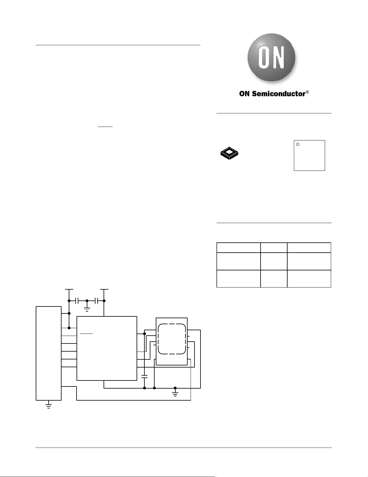
MPU or Microcontroller
SIM Card
Detect
GND
CC
GND
10
SIM_V
SIM_RST
NCN4555
SIM_CLK
SIM_I/O
CC
1
2
3
4
1mF
V
CC
RST
CLK
C4
DET DET
GND
7
9
11
8
GND
I/O
C8
5
6
7
8
Figure 1. Typical Interface Application
*For additional information on our Pb−Free strategy and soldering details, please
download the ON Semiconductor Soldering and Mounting Techniques
Reference Manual, SOLDERRM/D.
© Semiconductor Components Industries, LLC, 2010
October, 2010 − Rev. 3
1 Publication Order Number:
NCN4555/D
Page 2
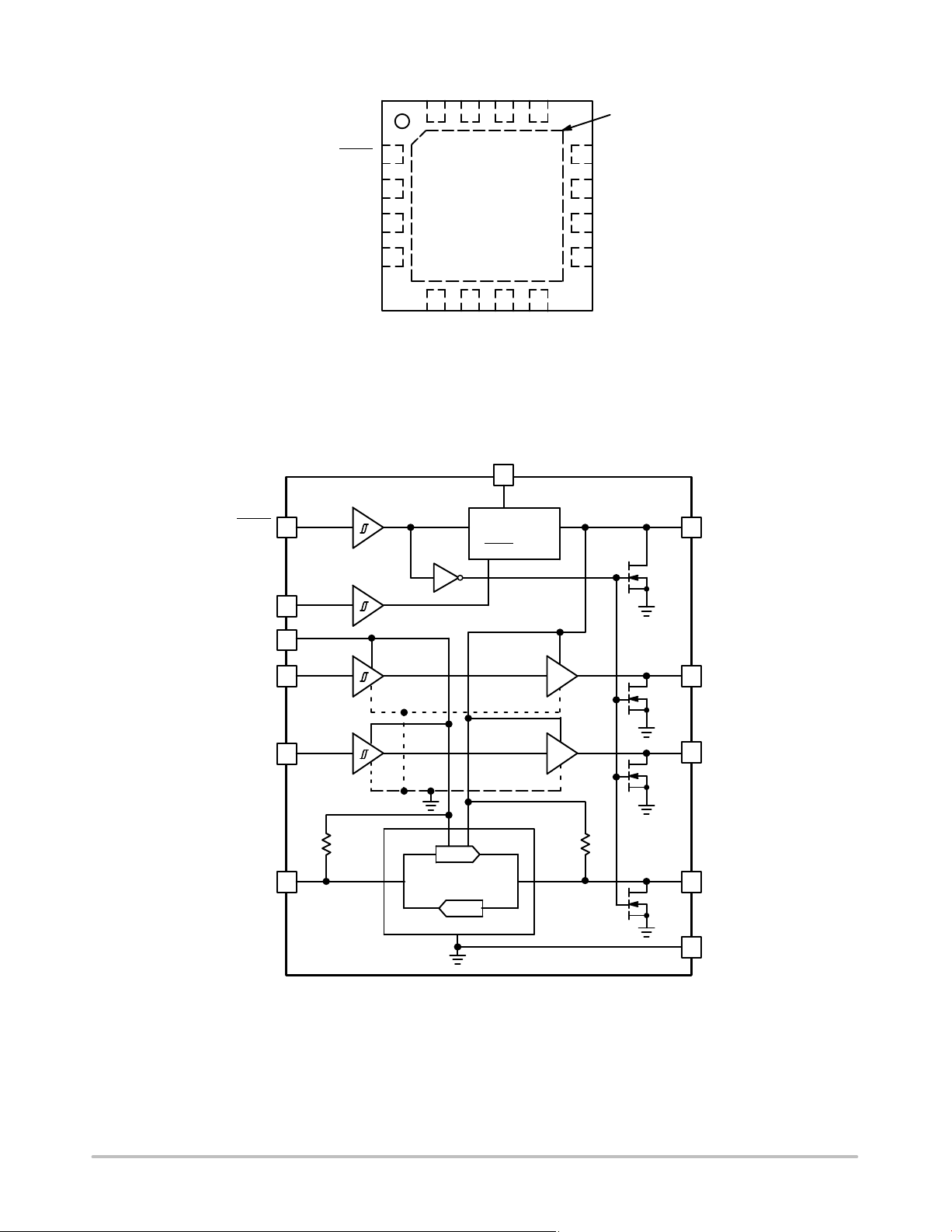
NCN4555
NC I/O RST CLK
16 15 14 13
Exposed Pad (EP)
STOP
MOD_V
CC
V
DD
(1.6 V to 5.5 V)
STOP
MOD_V
CC
1
2
12
11
NC
SIM_CLK
NCN4555
V
DD
NC
3
4
10
9
GND
SIM_RST
5678
V
NC SIM_VCCSIM_I/O
BAT
Figure 2. QFN−16 Pinout (Top View)
(2.7 V to 5.5 V)
V
BAT
5
GND
7
SIM_V
CC
1
50 mA LDO
1.8 V
/3.0 V
2
3
RST
CLK
I/O
14
13
15
GND
18 kW
I/O
DATADATA
I/O
GND
Figure 3. NCN4555 Block Diagram
14 kW
GND
GND
GND
9
11
8
10
SIM_RST
SIM_CLK
SIM_I/O
GND
http://onsemi.com
2
Page 3
NCN4555
PIN DESCRIPTIONS
PIN Name Type Description
1 STOP INPUT Power Down Mode pin:
2 MOD_V
3 V
DD
CC
INPUT The signal present on this pin programs the SIM_VCC value:
POWER This pin is connected to the system controller power supply. It configures the level shifter input
4 NC No Connect
5 V
BAT
POWER DC−DC converter supply input. The input voltage ranges from 2.7V up to 5.5V. This pin has to be
6 NC No Connect
7 SIM_V
CC
POWER This pin is connected to the SIM card power supply pin. An internal LDO converter is
8 SIM_I/O INPUT/
OUTPUT
9 SIM_RST OUTPUT This pin is connected to the RESET pin of the card connector. A level translator adapts the
10 GND GROUND This pin is the GROUND reference for the integrated circuit and associated signals. Care must be
11 SIM_CLK OUTPUT This pin is connected to the CLOCK pin of the card connector. The CLOCK (CLK) signal comes
12 NC No Connect
13 CLK INPUT The clock signal, coming from the external controller, must have a Duty Cycle within the Min/Max
14 RST INPUT The RESET signal present at this pin is connected to the SIM card through the internal level
15 I/O INPUT/
OUTPUT
16 NC No Connect
STOP
= Low ³ Low current shutdown mode activated
STOP
= High ³ Normal Operation
A Low level on this pin resets the SIM interface, switching off the SIM_V
MOD_V
MOD_V
= Low ³ SIM_VCC = 1.8 V
CC
= High ³ SIM_V
CC
CC
= 3 V
CC
.
stage to accept the signals coming from the microprocessor. A 0.1 mF capacitor shall be used to
bypass the power supply voltage. When V
NCN4555 comes into a shutdown mode.
is below 1.1 V typical the SIM_VCC is disabled. The
DD
bypass by a 0.1 mF capacitor.
programmable by the external MPU to supply either 1.8 V or 3.0 V output voltage. An external
1.0 mF minimum ceramic capacitor recommended must be connected across SIM_V
During a normal operation, the SIM_VCC voltage can be set to 1.8 V followed by a 3.0 V value, or
and GND.
CC
can start directly to any of these two values.
This pin handles the connection to the serial I/O of the card connector. A bidirectional level
translator adapts the serial I/O signal between the card and the micro controller. A 14 kW (typical)
pullup resistor provides a High impedance state for the SIM card I/O link.
external Reset (RST) signal to the SIM card.
taken to avoid voltage spikes when the device operates in a normal operation.
from the external clock generator, the internal level shifter being used to adapt the voltage defined
for the SIM_V
CC
.
values defined by the specification (typically 50%). The built−in level shifter translates the input
signal to the external SIM card CLK input.
shifter which translates the level according to the SIM_V
programmed value.
CC
This pin is connected to an external microcontroller or cellular phone management unit. A
bidirectional level translator adapts the serial I/O signal between the smart card and the external
controller. A built−in constant 18 kW (typical) resistor provides a high impedance state when not
activated.
http://onsemi.com
3
Page 4
NCN4555
ATTRIBUTES
Characteristics Values
ESD protection
HBM, SIM card pins (7, 8, 9, 10 & 11) (Note 1)
HBM, All other pins (Note 1)
MM, SIM card pins (7, 8, 9, 10 & 11) (Note 2)
MM, All other pins (Note 2)
CDM, SIM card pins (7, 8, 9, 10 & 11) (Note 3)
CDM , All other pins (Note 3)
Moisture sensitivity (Note 4) QFN−16 Level 1
Flammability Rating Oxygen Index: 28 to 34 UL 94 V−0 @ 0.125 in
Meets or exceeds JEDEC Spec EIA/JESD78 IC Latchup Test
1. Human Body Model, R =1500 W, C = 100 pF.
2. Machine Model.
3. CDM, Charged Device Model.
4. For additional information, see Application Note AND8003/D.
MAXIMUM RATINGS (Note 5)
Rating
LDO Power Supply Voltage V
Power Supply from Microcontroller Side V
External Card Power Supply SIM_V
Digital Input Pins V
Digital Output Pins V
SIM card Output Pins V
QFN−16 Low Profile package
Power Dissipation @ T
Thermal Resistance Junction−to−Air
= + 85°C
A
Operating Ambient Temperature Range T
Operating Junction Temperature Range T
Maximum Junction Temperature T
Storage Temperature Range T
Stresses exceeding Maximum Ratings may damage the device. Maximum Ratings are stress ratings only. Functional operation above the
Recommended Operating Conditions is not implied. Extended exposure to stresses above the Recommended Operating Conditions may affect
device reliability.
5. Maximum electrical ratings are defined as those values beyond which damage to the device may occur at T
Symbol Value Unit
BAT
DD
CC
in
I
in
out
I
out
out
I
out
P
D
R
q
JA
A
J
Jmax
stg
> 7 kV
> 2 kV
> 600 V
> 200 V
> 2 kV
> 600 V
−0.5 ≤ V
≤ 6 V
BAT
−0.5 ≤ VDD ≤ 6 V
−0.5 ≤ SIM_VCC ≤ 6 V
−0.5 ≤ Vin ≤V
but < 6.0
DD
+ 0.5
±5
−0.5 ≤ V
≤ VDD + 0.5
out
but < 6.0
±10
−0.5 ≤ V
≤ SIM_VCC + 0.5
out
but < 6.0
15 (internally limited)
440
90
−40 to +85 °C
−40 to +125 °C
+125 °C
−65 to + 150 °C
= +25°C
A
V
mA
V
mA
V
mA
mW
°C/W
http://onsemi.com
4
Page 5

NCN4555
POWER SUPPLY SECTION (−40°C to +85°C)
Pin
NOTE: Device will meet the specifications after thermal equilibrium has been established when mounted in a test socket or printed circuit
6. As long as V
7. As long as V
8. Guaranteed by design over the operating temperature range specified.
Symbol Rating Min Typ Max Unit
5 V
5 I
5 I
3 V
3 I
3 I
3 V
BAT
VBAT
VBAT_SD
DD
VDD
VDD_SD
DD
7 SIM_V
7 I
SIM_VCC_SC
Power Supply 2.7 5.5 V
Operating current – ICC = 0 mA (Note 6) 22 30
Shutdown current – STOP= Low (Note 7) 3.0
Operating Voltage 1.6 5.5 V
Operating Current – f
= 1 MHz (Note 8) 7.0 12
CLK
Shutdown Current – STOP = Low 1.0
Undervoltage Lockout 0.6 1.5 V
MOD_VCC = High, V
CC
MOD_V
MOD_VCC = Low, V
= High, V
CC
= 3.0 V, I
BAT
= 3.3 V to 5.5 V, I
BAT
= 2.7 V to 5.5 V, I
BAT
SIM_VCC
= 50 mA
SIM_VCC
SIM_VCC
= 0 mA to 50 mA
= 0 mA to 50 mA
2.8
1.7
2.8
3.0
1.8
Short –Circuit Current – SIM_VCC shorted to ground , TA=25°C 175 mA
3.2
1.9
board with maintained transverse airflow greater than 500 lfpm. Electrical parameters are guaranteed only over the declared
operating temperature range. Functional operation of the device exceeding these conditions is not implied. Device specification limit
values are applied individually under normal operating conditions and not valid simultaneously.
BAT
BAT
– V
– V
2.5 V. For V
v
DD
2.5 V.
v
DD
– VDD > 2.5 V the maximum value increases up to 35 mA (typical being in the +25 mA range).
BAT
mA
mA
mA
mA
V
V
V
DIGITAL INPUT/OUTPUT SECTION CLOCK, RESET, I/O, STOP, MOD_V
CC
Pin Symbol Rating Min Typ Max Unit
1,2, 13,
14, 15
13, 14 V
1, 2 V
15 V
15 R
V
IIH & I
IH
V
IL
IH
V
IL
OH_I/O
V
OL_I/O
I
IH
I
IL
pu_I/O
Input Voltage Range (STOP, MOD_VCC, RST, CLK, I/O)
in
Input Current (STOP
IL
, MOD_VCC, RST, CLK)
High Level Input Voltage (RST, CLK)
Low Level Input Voltage (RST, CLK)
High Level Input Voltage (STOP, MOD_VCC)
Low Level Input Voltage (STOP
, MOD_VCC)
High Level Output Voltage (SIM_I/O = SIM_VCC, I
Low Level Output Voltage (SIM_I/O = 0 V, I
High Level Input Current (I/O)
OH_I/O
= −20 mA)
OH_I/O
= 200 mA)
0
−100
0.7 * V
(Note 9)
0.7 * V
(Note 9)
0
0.7 * V
0
−20
DD
DD
DD
Low Level Input Current (I/O)
I/0 Pullup Resistor 12 18 24
V
100
V
0.4
V
0.4
V
0.4
20
1.0
DD
DD
DD
DD
mA
NOTE: Device will meet the specifications after thermal equilibrium has been established when mounted in a test socket or printed circuit
board with maintained transverse airflow greater than 500 lfpm. Electrical parameters are guaranteed only over the declared
operating temperature range. Functional operation of the device exceeding these conditions is not implied. Device specification limit
values are applied individually under normal operating conditions and not valid simultaneously.
9. If 1.6 V ≤ V
≤ 1.8 V then V
DD
IHmin
= 1.26 V.
V
nA
V
V
V
V
V
V
mA
kW
http://onsemi.com
5
Page 6

SIM INTERFACE SECTION (Note 10)
Pin
Symbol Rating Min Typ Max Unit
9 SIM_RST SIM_VCC = +3.0 V (MOD_VCC = High)
Output RESET V
Output RESET V
Output RESET Rise Time @ Cout = 30 pF
OH
OL
@ I
@ I
Output RESET Fall Time @ Cout = 30 pF
sim_rst
sim_rst
NCN4555
= −20 mA
= +200 mA
0.9 * SIM_V
0
CC
SIM_V
0.4
1
1
CC
V
V
ms
ms
SIM_V
= +1.8 V (MOD_VCC = Low)
CC
Output RESET V
Output RESET V
Output RESET Rise Time @ Cout = 30 pF
OH
OL
@ I
@ I
sim_rst
sim_rst
= −20 mA
= +200 mA
Output RESET Fall Time @ Cout = 30 pF
0.9 * SIM_V
0
CC
SIM_V
0.4
1
1
CC
11 SIM_CLK SIM_VCC = +3.0 V (MOD_VCC = High)
SIM_V
Output Duty Cycle
Max Output Frequency
Output V
Output V
Output SIM_CLK Rise Time @ Cout = 30 pF
OH
OL
@ I
@ I
sim_clk
sim_clk
= −20 mA
= +200 mA
Output SIM_CLK Fall Time @ Cout = 30 pF
= +1.8 V (MOD_VCC = Low)
CC
Output Duty Cycle
Max Output Frequency
Output V
Output V
Output SIM_CLK Rise Time @ Cout = 30 pF
OH
OL
@ I
@ I
sim_clk
sim_clk
= −20 mA
= +200 mA
Output SIM_CLK Fall Time @ Cout = 30 pF
40
5
0.9 * SIM_V
0
40
5
0.9 * SIM_V
0
CC
CC
60
SIM_V
0.4
18
18
60
SIM_V
0.4
18
18
MHz
CC
MHz
CC
8 SIM_I/O SIM_VCC = +3.0 V (MOD_VCC = High)
8 R
pu_SIM_I/O
Output V
Output VOL @ I
SIM_I/O Rise Time @ C
OH
@ I
SIM_IO
SIM_IO
SIM_I/O Fall Time @ C
SIM_V
Output V
Output VOL @ I
SIM_I/O Rise Time @ C
= +1.8 V (MOD_VCC = High)
CC
@ I
OH
SIM_IO
SIM_IO
SIM_I/O Fall Time @ C
= −20 mA, V
= +1 mA, V
= 30 pF
out
= 30 pF
out
= −20 mA, V
= +1.0 mA, V
= 30 pF
out
= 30 pF
out
I/O
I/O
I/O
= V
= 0 V
=V
= 0 V
I/O
DD
DD
0.8 * SIM_V
0
0.8 * SIM_V
0
CC
CC
Card I/O Pullup Resistor 10 14 18
SIM_V
0.4
1
1
SIM_V
0.3
1
1
CC
CC
NOTE: Device will meet the specifications after thermal equilibrium has been established when mounted in a test socket or printed circuit
board with maintained transverse airflow greater than 500 lfpm. Electrical parameters are guaranteed only over the declared
operating temperature range. Functional operation of the device exceeding these conditions is not implied. Device specification limit
values are applied individually under normal operating conditions and not valid simultaneously.
10.All the dynamic specifications (AC specifications) are guaranteed by design over the operating temperature range.
V
V
ms
ms
%
V
V
ns
ns
%
V
V
ns
ns
V
V
ms
ms
V
V
ms
ms
kW
http://onsemi.com
6
Page 7

NCN4555
TYPICAL CHARACTERISTICS
100
V
= 5.5 V
V
BAT
BAT
= 2.7 V
90
80
70
IVCC_SC_1.8 V (mA)
60
50
−50 −30 −10 10 30 50 70 90
TEMPERATURE (°C)
Figure 4. Short Circuit Current IVCC_SC vs
Temperature at SIM_V
30
V
= 3.3 V
V
BAT
BAT
= 5.5 V
25
20
= 1.8 V (MOD_VCC = LOW)
CC
100
V
= 5.5 V
90
80
70
IVCC_SC_3.0 V (mA)
60
50
−50 −30 −10 10 30 50 70 90
BAT
V
= 3.3 V
BAT
TEMPERATURE (°C)
Figure 5. Short Circuit Current IVCC_SC vs
Temperature at SIM_V
30
25
20
= 3.0 V (MOD_VCC = HIGH)
CC
V
= 2.7 V
BAT
V
= 5.5 V
BAT
IVCC_SC_3.0 V (mA)
15
10
−50 −30 −10 10 30 50 70 90
TEMPERATURE (°C)
Figure 6. I
vs temperature at 3.0 V
BAT
IVCC_SC_1.8 V (mA)
15
10
−50 −30 −10 10 30 50 70 90
TEMPERATURE (°C)
Figure 7. IV
vs Temperature at 1.8 V
BAT
http://onsemi.com
7
Page 8

NCN4555
APPLICATION INFORMATION
CARD SUPPLY CONVERTER
The NCN4555 interface DC−DC converter is a
Low Dropout Voltage Regulator capable of suppling a
current in excess of 50 mA under 1.8 V or 3.0 V. This device
features a very low quiescent current typically lower than
25 mA (Figure 6 and 7). MOD_V
is a select input
CC
allowing a logic level signal to select a regulated voltage of
1.8 V (MOD_V
= LOW) or 3.0 V (MOD_VCC = HIGH).
CC
Additionally, the NCN4555 has a shutdown input allowing
it to turn off or turn on the regulator output. The shutdown
mode power consumption is typically in the range of a few
tens of nA (30 nA Typical). Figure 8 shows a simplified
view of the NCN4555 voltage regulator. The SIM_V
CC
output is internally current limited and protected against
short circuits. The short−circuit current IV
over the temperature and SIM_V
. It varies with V
CC
is constant
CC
BAT
typically in the range of 60 mA to 90 mA (Figure 4 and 5).
V
BAT
I
Q1
lim
In order to guarantee a stable and satisfying operating of
the LDO the SIM_V
output will be connected to a 1.0 mF
CC
bypass ceramic capacitor to the ground. At the input, V
will be bypassed to the ground with a 0.1 mF ceramic
capacitor.
LEVEL SHIFTERS
The level shifters accommodate the voltage difference
that might exist between the microcontroller and the smart
card. The RESET and CLOCK level shifters are
monodirectional and feature both the same architecture.
The bidirectional I/O line provides a way to automatically
adapt the voltage difference between the MCU and the SIM
card in both directions. In addition with the pullup resistor,
an active pullup circuit (Figure 8, Q1 and Q2) provides a fast
charge of the stray capacitance, yielding a rise time fully
within the ISO7816 specifications.
SIM_V
CC
R1
−
BAT
CIN = 0.1 mF
STOP
V
DD
+
+
V
REF
R2
GND
Figure 8. Simplified Block Diagram of the LDO Voltage Regulator
Q1
18 k 14 k
200 ns200 ns
GND
Q2
Q3
C
OUT
SIM_V
SIM_I/OI/O
= 1.0 mF
MOD_V
CC
CC
LOGICIO/CONTROL
Figure 9. Basic I/O Line Interface
http://onsemi.com
8
GND
Page 9

NCN4555
The typical waveform provided in Figure 10 shows how
the accelerator operates. During the first 200 ns (typical),
the slope of the rise time is solely a function of the pullup
resistor associated with the stray capacitance. During this
period, the PMOS devices are not activated since the input
voltage is below their V
crosses the V
, the opposite one shot is activated,
gsth
threshold. When the input slope
gs
providing a low impedance to charge the capacitance, thus
increasing the rise time as depicted in Figure 10. The same
mechanism applies for the opposite side of the line to make
sure the system is optimum.
INPUT SCHMITT TRIGGERS
All the Logic input pins (excepted I/O and SIM_I/O, See
Figure 3) have built−in Schmitt trigger circuits to prevent
the NCN4555 against uncontrolled operation. The typical
dynamic characteristics of the related pins are depicted
Figure 11.
The output signal is guaranteed to go High when the input
voltage is above 0.7 x V
, and will go Low when the input
DD
voltage is below 0.4 V.
SHUTDOWN OPERATING
In order to save power or for other purpose required by the
application it is possible to put the NCN4555 in a shutdown
mode by setting Low the pin STOP
device enters automatically in a shutdown mode when V
. On the other hand the
DD
becomes lower than 1.1 V typically.
ESD PROTECTION
The NCN4555 SIM interface features an HBM ESD
voltage protection in excess of 7 kV for all the SIM pins
(SIM_IO, SIM_CLK, SIM_RST, SIM_V
and GND). All
CC
the other pins (microcontroller side) sustain at least 2 kV.
These values are guaranteed for the device in its full integrity
without considering the external capacitors added to the
circuit for a proper operating. Consequently in the operating
conditions it is able to sustain much more than 7 kV on its
SIM pins making it perfectly protected against electrostatic
discharge well over the HBM ESD voltages required by the
ISO7816 standard (4 kV).
PRINTED CIRCUIT BOARD LAYOUT
Careful layout routing will be applied to achieve a good
and efficient operating of the device in its mobile or portable
environment and fully exploit its performance.
The bypass capacitors have to be connected as close as
possible to the device pins (SIM_V
, VDD or V
CC
BAT
) in
order to reduce as much as possible parasitic behaviors
(ripple and noise). It is recommended to use
ceramic capacitors.
The exposed pad of the QFN−16 package will be
connected to the ground as well as the unconnected pins
(NC). A relatively large ground plane is recommended.
Figures 12 and 13 shows an example of PCB device
implementation in an evaluation environment.
Figure 10. SIM_IO Typical Rise and Fall Times with
Stray Capacitance > 30 pF
(33 pF Capacitor Connected on the Board)
OUTPUT
V
DD
ON
OFF
INPUT
0.2 x V
or 0.4 V
Figure 11. Typical Schmitt Trigger Characteristics
DD
0.7 x V
DD
http://onsemi.com
9
Page 10

NCN4555
EVALUATION BOARD AND PCB GUIDELINES
NC
NCNC
IP8
SIM_I/O
876
C8
C4
4
1
3
I/O
CLK
2
5
DD
V
RST
1
GND
SIM_CARD
CC
V
DD
V
2.2 k
R5
R6
2N2222
Q1
GND
POI2
GND
SIM_RST
SIM_CLK
DD
IP10
V
MOD
STOP
I/O
IP3 IP4 IP5
IP2
RST
IP1
CLK
CLK
J1
IP7
11
IP6
C2
V2
1
MBRA140T3
111
111
SIM_CLK
SIM_I/O
SIM_RST
12119810
NC
SIM_CLK
DD
V
CLK
3
10 mF
DD
V
131415
D3
GND
SIM_I/O
SIM_RST
RST
I/O
NC
16
GND_EXP
124
2
DD
V
GND
MOD_V
STOP
SIM_V
6
CC
NC NC
V
CC
J8
7
CC
SIM_V
BAT
V
5
BAT
MBRA140T3
D4
CON2
2.2 k
2
SENSE_SIM_V
IP9
BATD1
V
R1
C1100 nF
BAT
V1
V
1
CC
GNDGND GND
GND
J10 J11
GND GND
1
R2
R3
10 k
J2
RST
J3
I/O
10 k
STOP
J4
MOD_V
2
STOP
2
CC
MOD_V
J5
CC
1
S2
J9
GND
GND
1
S1
NC
NC
NC
NC
NC
NC
NC
12
11
10
9
8
7
6
5
4
3
2
1
CONTROL & I/O
J6
GNDGNDGNDGNDGND
Figure 12. NCN4555 engineering test board schematic diagram
http://onsemi.com
10
Page 11

NCN4555
EVALUATION BOARD AND PCB GUIDELINES
Top Layer
Bottom Layer
Figure 13. NCN4555 Printed Circuit Board Layout
(Engineering board)
http://onsemi.com
11
Page 12

MECHANICAL CASE OUTLINE
PACKAGE DIMENSIONS
1
SCALE 2:1
16 X
LOCATION
0.10 C
0.08 C
16X
NOTE 5
16X
0.10 C
0.05 C
PIN 1
0.15 C
0.15
L
K
16X
A B
NOTE 3
D
TOP VIEW
C
SIDE VIEW
D2
58
4
1
16 13
b
BOTTOM VIEW
(A3)
e
9
12
A
B
E
A1
EXPOSED PAD
QFN16 3*3*0.75 MM, 0.5 P
CASE 488AK−01
ISSUE O
A
SEATING
PLANE
C
E2
DATE 13 SEP 2004
NOTES:
1. DIMENSIONING AND TOLERANCING PER
ASME Y14.5M, 1994.
2. CONTROLLING DIMENSION: MILLIMETERS.
3. DIMENSION b APPLIES TO PLATED
TERMINAL AND IS MEASURED BETWEEN
0.25 AND 0.30 MM FROM TERMINAL.
4. COPLANARITY APPLIES TO THE EXPOSED
PAD AS WELL AS THE TERMINALS.
CONDITION CAN NOT VIOLATE 0.2 MM
5. L
max
SPACING BETWEEN LEAD TIP AND FLAG.
MILLIMETERS
DIM MIN MAX
A 0.70 0.80
A1 0.00 0.05
A3 0.20 REF
b 0.18 0.30
D 3.00 BSC
D2 1.65 1.85
E 3.00 BSC
E2 1.65 1.85
e 0.50 BSC
K 0.20 −−−
L 0.30 0.50
GENERIC
MARKING DIAGRAM*
16
1
XXXX
XXXX
ALYW
XXXX = Specific Device Code
A = Assembly Location
L = Wafer Lot
Y = Year
W = Work Week
*This information is generic. Please refer
to device data sheet for actual part
marking. Pb−Free indicator, “G”, may
or not be present.
DOCUMENT NUMBER:
DESCRIPTION:
ON Semiconductor and are trademarks of Semiconductor Components Industries, LLC dba ON Semiconductor or its subsidiaries in the United States and/or other countries.
ON Semiconductor reserves the right to make changes without further notice to any products herein. ON Semiconductor makes no warranty, representation or guarantee regarding
the suitability of its products for any particular purpose, nor does ON Semiconductor assume any liability arising out of the application or use of any product or circuit, and specifically
disclaims any and all liability, including without limitation special, consequential or incidental damages. ON Semiconductor does not convey any license under its patent rights nor the
rights of others.
© Semiconductor Components Industries, LLC, 2019
98AON19612D
QFN16, 3*3*0.75 MM, 0.5 PITCH
Electronic versions are uncontrolled except when accessed directly from the Document Repository.
Printed versions are uncontrolled except when stamped “CONTROLLED COPY” in red.
PAGE 1 OF 1
www.onsemi.com
Page 13

ON Semiconductor and are trademarks of Semiconductor Components Industries, LLC dba ON Semiconductor or its subsidiaries in the United States and/or other countries.
ON Semiconductor owns the rights to a number of patents, trademarks, copyrights, trade secrets, and other intellectual property. A listing of ON Semiconductor’s product/patent
coverage may be accessed at www.onsemi.com/site/pdf/Patent−Marking.pdf
ON Semiconductor makes no warranty, representation or guarantee regarding the suitability of its products for any particular purpose, nor does ON Semiconductor assume any liability
arising out of the application or use of any product or circuit, and specifically disclaims any and all liability, including without limitation special, consequential or incidental damages.
Buyer is responsible for its products and applications using ON Semiconductor products, including compliance with all laws, regulations and safety requirements or standards,
regardless of any support or applications information provided by ON Semiconductor. “Typical” parameters which may be provided in ON Semiconductor data sheets and/or
specifications can and do vary in different applications and actual performance may vary over time. All operating parameters, including “Typicals” must be validated for each customer
application by customer’s technical experts. ON Semiconductor does not convey any license under its patent rights nor the rights of others. ON Semiconductor products are not
designed, intended, or authorized for use as a critical component in life support systems or any FDA Class 3 medical devices or medical devices with a same or similar classification
in a foreign jurisdiction or any devices intended for implantation in the human body. Should Buyer purchase or use ON Semiconductor products for any such unintended or unauthorized
application, Buyer shall indemnify and hold ON Semiconductor and its officers, employees, subsidiaries, affiliates, and distributors harmless against all claims, costs, damages, and
expenses, and reasonable attorney fees arising out of, directly or indirectly, any claim of personal injury or death associated with such unintended or unauthorized use, even if such
claim alleges that ON Semiconductor was negligent regarding the design or manufacture of the part. ON Semiconductor is an Equal Opportunity/Affirmative Action Employer. This
literature is subject to all applicable copyright laws and is not for resale in any manner.
. ON Semiconductor reserves the right to make changes without further notice to any products herein.
PUBLICATION ORDERING INFORMATION
LITERATURE FULFILLMENT:
Email Requests to: orderlit@onsemi.com
ON Semiconductor Website: www.onsemi.com
TECHNICAL SUPPORT
North American Technical Support:
Voice Mail: 1 800−282−9855 Toll Free USA/Canada
Phone: 011 421 33 790 2910
Europe, Middle East and Africa Technical Support:
Phone: 00421 33 790 2910
For additional information, please contact your local Sales Representative
◊
www.onsemi.com
1
 Loading...