

Page 1
NCL30073LED4GEVB
15 W High Power Factor
LED Driver
Evaluation Board
User'sManual
Overview
This manual covers the specification, theory of operation,
testing and construction of the NCL30073LED4GEVB
evaluation board. The NCL30073 board demonstrates a
15 W high PF buck boost LED driver for a typical downlight
application.
Key Features
The key features of this evaluation board include:
• Low Parts Count
• TRIAC Dimmer Compatible
• High Power Factor
• Integrated Fault Protection
♦ Over Temperature on board (a PCB mounted PTC)
♦ Output Over Current
♦ Output Over Voltage
www.onsemi.com
EVAL BOARD USER’S MANUAL
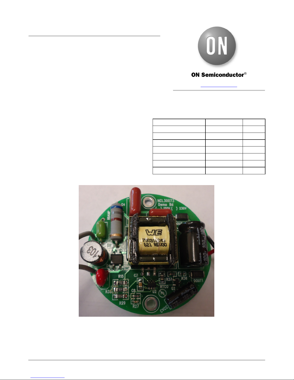
Table 1. SPECIFICATIONS
Input voltage 207 − 253 V ac
Line Frequency 50 Hz
Power Factor (100% Load)
Output Voltage 72 V dc
Output Ripple 75% Pk − Pk
Output Current 200 mA dc ± 5%
Efficiency 88.5% Typ.
Start Up Time < 250 msec Typ.
0.9
Min
© Semiconductor Components Industries, LLC, 2017
July, 2017 − Rev. 0
Figure 1. Evaluation Board Photo
1 Publication Order Number:
EVBUM2505/D
Page 2
NCL30073LED4GEVB
THEORY OF OPERATION
Power Stage
The power stage is a flying buck boost design. In this
configuration, drain of the switching FET is connected to the
rectified HVDC and the source is switching. This has many
benefits:
1. Direct output current sensing
2. Direct output voltage sensing
3. No Aux winding needed
The power stage operates as a fixed frequency DCM
power stage. The DCM allows for no forced commutation
of the output diode for good EMI performance. The fixed
current/fixed frequency provides for a constant power
control over a large portion of the input waveform. The
resistor divider of R27 and R29 provides some wave shaping
to improve the power factor. The input current waveform is
made to be square for maximum TRIAC dimmer
compatibility.
Figure 2.
Output Voltage Sense and Vcc generation
Dout1 is in parallel with the output during the off time of
the FET and stores energy in Cvcc. R36 and R37 divide the
output voltage and Q2 buffers it to provide Vcc power to the
controller. Since the divider is a fixed ratio, Vcc is a fixed
percentage of the output voltage. When Vcc rises above
25 V, the controller detects and OVP fault. The maximum
output voltage is set by adjusting the ratio of R36/R37.
In cases where the output has a lot of ripple current and the
LED has high dynamic resistance, the peak output voltage
can be much higher than the average output voltage. The
inductor winding will charge the Cvcc to the peak of the
output voltage which may trigger the OVP sooner than
expected so in this case the peak voltage of the LED string
is critical.
Protection
Thermal Protection
Rtco is a PTC connected between the CS pin and Rsens.
The controller creates and internal signal current from the
CS pin. As the resistance of Rtco becomes larger with
temperature, the signal level at the CS pin increases causing
the current to foldback with temperature.
Programmable OVP
R36 and R37 set Vcc as a fixed percentage of the output
voltage. The OVP threshold on the controller is 25 V. So the
ratio of R36/R37 is set to trip the Vcc OVP threshold at about
100 V output.
Overcurrent Protection
The controller has built in overcurrent limits.
Output Current
The output current is set by the value of Rsens. It’s
possible to adjust the output current by changing Rsens.
TRIAC Dimming Compatibility
The EMI filter components are selected to provide
optimum damping of the EMI filter to eliminate ringback of
the input current which will lead to loss of hold current in the
dimmer. The square nature of the input current makes the
best case for TRIAC holding current over the line cycle
while still maintaining power factor above 0.9.
www.onsemi.com
2
Page 3
NCL30073LED4GEVB
SCHEMATIC
+HVDC_iso
AC_L
AC_N
+HVDC_iso
CVcc
10uF 100V
1
1
Dout1
MURA160T3G
R36
301k
F2
0A5
R37
100k
Q2
MMBT5551LT1G
RV1
MOV 250V
C8
10nF
412k
R29
L1
10mH
1
OPP
2
FB
3
CS
NCL30073
R27
10k
D4
+
AC1
−
AC2
MB6S
Figure 3. Input Circuit
R15
143k
R38
220k
U2
6
Vcc
5
Gdrv
4
Gnd
1uF 50V
C7
Rtco
680 PTC
C4
100nF 400V
Rdamp
680
C6
33nF 400V
Q1
NDD60N900U1T4G
t
Rsens
1.13
Dout
MURA160T3G
1
LED−
Cout
100uF100V
Figure 4. Main Circuit
www.onsemi.com
3
L5
1.2mH
1
LED+
Page 4
NCL30073LED4GEVB
BILL OF MATERIAL
Table 2. BILL OF MATERIAL
Refer-
ence
CVcc 1
Cout 1
C4 1 100 nF 400 V Faratronic C212G104−4B****+++ Faratronic C212G104−4B****+++ Yes
C6 1 33 nF 400 V Faratronic C212G333−3A****+++ Faratronic C212G333−3A****+++ Yes
C7 1
C8 1 10 nF Yageo CC0603KRX7R9BB1
Dout1,
Dout
D4 1 MB6S MCC MB6S Digikey MB4S−TPMSCT−ND Yes
F2 1 0A5 Littelfuse 0263.500WRT1L Digikey F1999CT−ND Yes
L1 1 10 mH Wurth 744772103 Digikey 732−3791−ND Yes
L5 1 1.2 mH Wurth 750316243 Wurth 750316243 Yes
Q1 1 NDD60N900U1T4G ON
Q2 1 MMBT5551LT1G ON
RV1 1 MOV 250V Littelfuse V390ZA05P Digikey F3361−ND Ye s
Rdamp 1 680 Yageo RSF200JB−73−680R Digikey 680W−2−ND Yes
Rsens 1 1.13 Yageo RC1206FR−071R13L Digikey 311−1.13FRCT−ND Ye s
Rtco 1 680 PTC Epcos B59721A90A62 Digikey 495−4312−1−ND Ye s
R15 1 143k Yageo RC1206FR−07143KL Digikey 311−143KFRCT−ND Ye s
R27 1 10k Yageo RC0603FR−0710k0L Digikey 311−10.0KHRCT−ND Yes
R29 1 412k Yageo RC1206FR−07412KL Digikey 311−412KFRCT−ND Ye s
R36 1 301k Yageo RC0603FR−07301KL Digikey 311−301KHRCT−ND Yes
R37 1 100k Yageo RC0603FR−07100KL Digikey 311−100KHRCT−ND Yes
R38 1 220k Yageo RC1206FR−07220KL Digikey 311−220KFRCT−ND Ye s
U2 1 NCL30073 ON
Qty Part Distributor
10 mF 100 V
100 mF 100 V
1 mF 50 V
2 MURA160T3G ON
Rubycon 100YXJ10M5X11 Digikey
Nichicon UVK2A101MPD Digikey
Yageo CC0805KKX7R9BB1
Semiconductor
Semiconductor
Semiconductor
Semiconductor
Distributor
Part Number
05
03
MURA160T3G ON
NDD60N900U1T4G ON
MMBT5551LT1G ON
NCL30073 ON
Manufacturer
Digikey 311−1886−1−ND Yes
Digikey 311−1085−1−ND Yes
Semiconductor
Semiconductor
Semiconductor
Semiconductor
Manufacturer
Part Number
1189−2150−ND
UVK2A101MPD−ND
MURA160T3G No
NDD60N900U1T4G No
MMBT5551LT1G No
NCL30073 No
Substitution
Allowed
Yes
Yes
NOTE: All components to comply with RoHS 2002/95/EC
www.onsemi.com
4
Page 5

NCL30073LED4GEVB
GERBER VIEWS
Figure 5. Top Side PCB
www.onsemi.com
5
Page 6

NCL30073LED4GEVB
Circuit Board Fabrication Notes
1. Fabricate per IPC−6011 and IPC6012. Inspect to
IPA−A−600 Class 2 or updated standard.
2. Printed Circuit Board is defined by files listed in
fileset.
3. Modification to copper within the PCB outline is
not allowed without permission, except where
noted otherwise. The manufacturer may make
adjustments to compensate for manufacturing
process, but the final PCB is required to reflect the
associated gerber file design ± 0.001 in. for etched
features within the PCB outline.
4. Material in accordance with IPC−4101/21, FR4,
Tg 125°C min.
5. Layer to layer registration shall not exceed
± 0.004 in.
6. External finished copper conductor thickness shall
be 0.0026 in. min. (ie 2oz)
7. Copper plating thickness for through holes shall be
0.0013 in. min. (ie 1oz)
8. All holes sizes are finished hole size.
9. Finished PCB thickness 0.062 in.
10. All un-dimensioned holes to be drilled using the
NC drill data.
Figure 6. PCB Outline
11. Size tolerance of plated holes: ± 0.003 in. :
non−plated holes ± 0.002 in.
12. All holes shall be ± 0.003 in. of their true position
U.D.S.
13. Construction to be SMOBC, using liquid photo
image (LPI) solder mask in accordance with
IPC−SM−B40C, Type B, Class 2, and be green in
color.
14. Solder mask mis-registration ± 0.004 in. max.
15. Silkscreen shall be permanent non−conductive
white ink.
16. The fabrication process shall be UL approved and
the PCB shall have a flammability rating of
UL94V0 to be marked on the solder side in
silkscreen with date, manufactures approved logo,
and type designation.
17. Warp and twist of the PCB shall not exceed
0.0075 in. per in.
18. 100% electrical verification required.
19. Surface finish: electroless nickel immersion gold
(ENIG)
20. RoHS 2002/95/EC compliance required.
www.onsemi.com
6
Page 7

NCL30073LED4GEVB
ECA PICTURES
Figure 7. Top View
www.onsemi.com
7
Page 8

NCL30073LED4GEVB
TEST PROCEDURE
Equipment Needed
• AC Source – 200 to 260 V ac 50 Hz Minimum 100 W
capability
• AC Wattmeter – 100 W Minimum, True RMS Input
Voltage, Current, Power Factor, and THD 0.2%
accuracy or better
• DC Voltmeter – 300 V dc minimum 0.1% accuracy or
better
• DC Ammeter – 1 A dc minimum 0.1% accuracy or
better
• LED Load – 70 V – 80 V @ 110 mA
AC Power
Source
Note: Unless otherwise specified, all voltage measurements are taken at the terminals of the UUT.
Functional Test Procedure
1. Set the LED Load for 75 V output.
2. Set the input power to 230 V 50 Hz.
Caution: Do not touch the ECA once it is
energized because there are hazardous voltages
present.
AC
Wattmeter
Figure 8. Test Set Up
Test Connections
1. Connect the LED Load to the red(+) and black(−)
2. Connect the AC power to the input of the AC
3. Connect the DC voltmeter as shown in Figure 8.
UUT
Regulation
230 V / Max Load
leads through the ammeter shown in Figure 10.
Caution: Observe the correct polarity or the
load may be damaged.
wattmeter shown in Figure 8. Connect the white
leads to the output of the AC wattmeter
DC Ammeter
DC Voltmeter
LED Test
Load
Table 3.
207 V
230 V
253 V
Efficiency +
Vout Iout
Pin
Output Current Output Power Power Factor THD
100%
www.onsemi.com
8
Page 9

NCL30073LED4GEVB
TEST DATA
Figure 9. Power Factor Over Line
Figure 10. THD Over Line
www.onsemi.com
9
Page 10

NCL30073LED4GEVB
Figure 11. Efficiency
Figure 12. Regulation Over Line
www.onsemi.com
10
Page 11

NCL30073LED4GEVB
Figure 13. Start Up with AC Applied 230 V
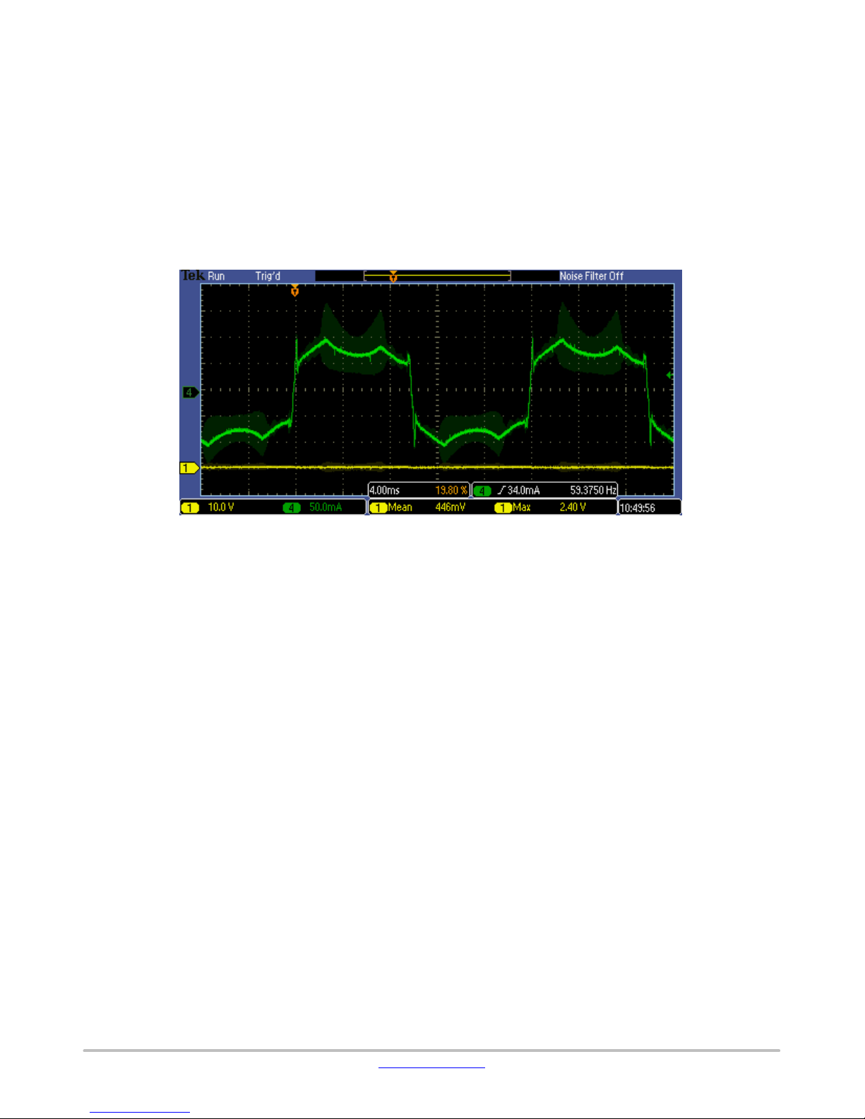
Figure 14. Output Ripple 75% Pk − Pk
www.onsemi.com
11
Page 12

NCL30073LED4GEVB
Figure 15.
Q1
R15, R29, R38
Figure 16. Thermal Image SMT Side
www.onsemi.com
12
Page 13

NCL30073LED4GEVB
ON Semiconductor and are trademarks of Semiconductor Components Industries, LLC dba ON Semiconductor or its subsidiaries in the United States and/or other countries.
ON Semiconductor owns the rights to a number of patents, trademarks, copyrights, trade secrets, and other intellectual property. A listing of ON Semiconductor’s product/patent
coverage may be accessed at www.onsemi.com/site/pdf/Patent−Marking.pdf
ON Semiconductor makes no warranty, representation or guarantee regarding the suitability of its products for any particular purpose, nor does ON Semiconductor assume any liability
arising out of the application or use of any product or circuit, and specifically disclaims any and all liability, including without limitation special, consequential or incidental damages.
Buyer is responsible for its products and applications using ON Semiconductor products, including compliance with all laws, regulations and safety requirements or standards,
regardless of any support or applications information provided by ON Semiconductor. “Typical” parameters which may be provided in ON Semiconductor data sheets and/or
specifications can and do vary in different applications and actual performance may vary over time. All operating parameters, including “Typicals” must be validated for each customer
application by customer’s technical experts. ON Semiconductor does not convey any license under its patent rights nor the rights of others. ON Semiconductor products are not
designed, intended, or authorized for use as a critical component in life support systems or any FDA Class 3 medical devices or medical devices with a same or similar classification
in a foreign jurisdiction or any devices intended for implantation in the human body. Should Buyer purchase or use ON Semiconductor products for any such unintended or unauthorized
application, Buyer shall indemnify and hold ON Semiconductor and its officers, employees, subsidiaries, affiliates, and distributors harmless against all claims, costs, damages, and
expenses, and reasonable attorney fees arising out of, directly or indirectly, any claim of personal injury or death associated with such unintended or unauthorized use, even if such
claim alleges that ON Semiconductor was negligent regarding the design or manufacture of the part. ON Semiconductor is an Equal Opportunity/Affirmative Action Employer. This
literature is subject to all applicable copyright laws and is not for resale in any manner.
PUBLICATION ORDERING INFORMATION
LITERATURE FULFILLMENT:
Literature Distribution Center for ON Semiconductor
19521 E. 32nd Pkwy, Aurora, Colorado 80011 USA
Phone: 303−675−2175 or 800−344−3860 Toll Free USA/Canada
Fax: 303−675−2176 or 800−344−3867 Toll Free USA/Canada
Email: orderlit@onsemi.com
◊
. ON Semiconductor reserves the right to make changes without further notice to any products herein.
N. American Technical Support: 800−282−9855 Toll Free
USA/Canada
Europe, Middle East and Africa Technical Support:
Phone: 421 33 790 2910
Japan Customer Focus Center
Phone: 81−3−5817−1050
www.onsemi.com
ON Semiconductor Website: www.onsemi.com
Order Literature: http://www.onsemi.com/orderlit
For additional information, please contact your local
Sales Representative
EVBUM2505/D
13
 Loading...