

Page 1
NCD9830GEVB
NCD9830 Evaluation Board
User's Manual
About This Manual
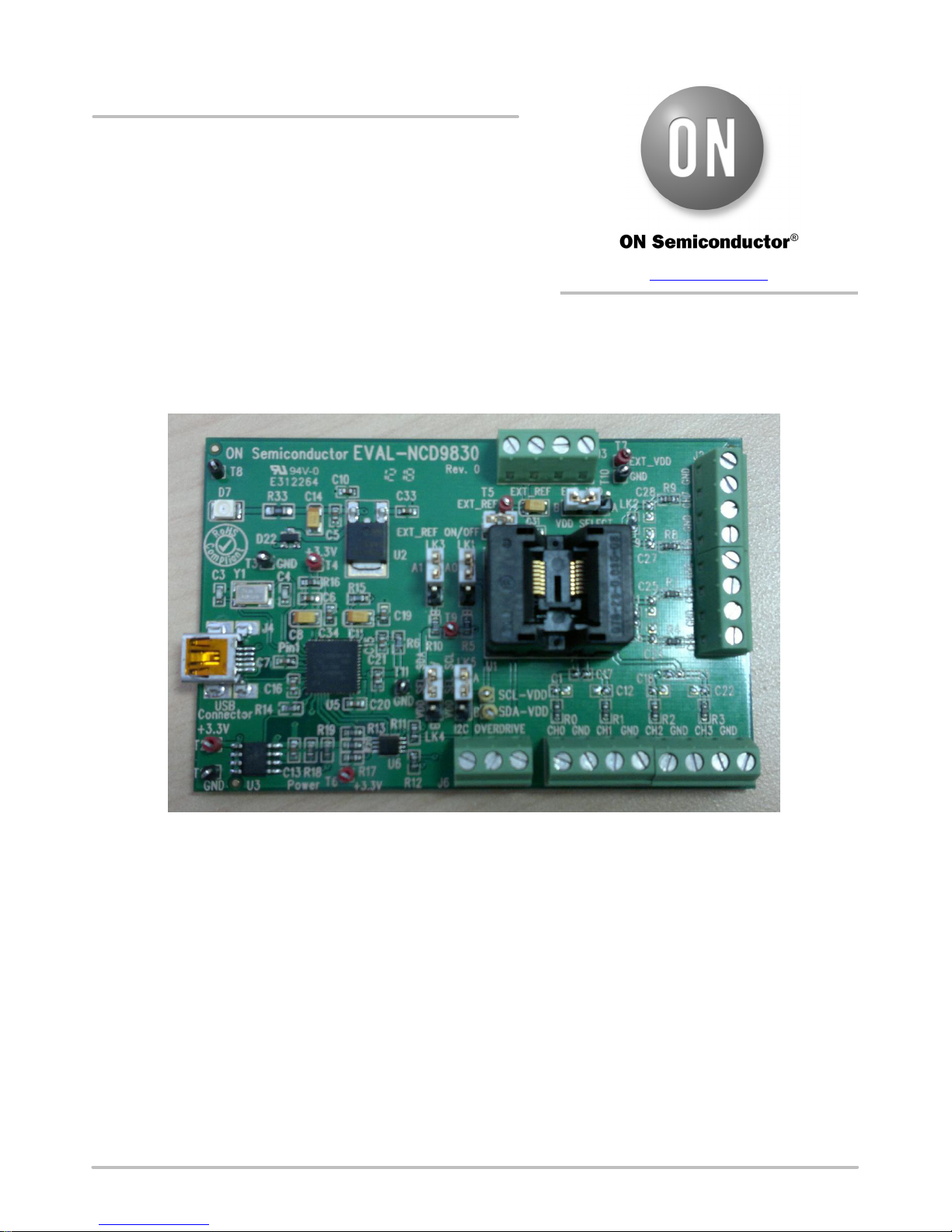
This manual will enable the user to use NCD9830
Evaluation Board to evaluate functional performance of
NCD9830. A TSSOP−16 socket is available on the board to
avoid the hassle of soldering the device. NCD9830 is tested
by using a digital interface cable along with the supported
software. The test results should be taken to judge the device
functional performance according the specification in the
technical datasheet.
www.onsemi.com
EVAL BOARD USER’S MANUAL
NCD9830 Product Information
The NCD9830 is a classic successive approximation
analog to digital converter with 8 bit resolution and an
internal 8 channel multiplexer. The converter contains
a capacitive DAC that eliminates the need of a separate
sample and hold circuit. The device has the capabilty to
generate an internal reference voltage for the built-in DAC.
Fast conversion time, low power dissipation and low noise
makes this device ideal for applications like sensors data
acquisition, battery monitoring, remote actuator interface
and gaming consoles/modules and telecommunications.
Communication with the NCD9830 is accomplished via the
2
I
C interface which is compatible with industry standard
© Semiconductor Components Industries, LLC, 2014
October, 2014 − Rev. 0
Figure 1. NCD9830 Evaluation Board
protocols. The NCD9830 is available in a 16 lead TSSOP
package.
Features
• 8 Bit Resolution with Internal 8 channel Multiplexer
• Low Power Operation with Guaranteed Low Noise
SNR
• No Missing Codes and Fast Conversion Time
• Internally Generated Clock and Reference Voltage
• Operational Supply Voltage from 2.7 to 5.5 V
• Meets I
2
C Standard, Fast and High Speed Operation
• Full ROHS Compliant
1 Publication Order Number:
EVBUM2270/D
Page 2
NCD9830GEVB
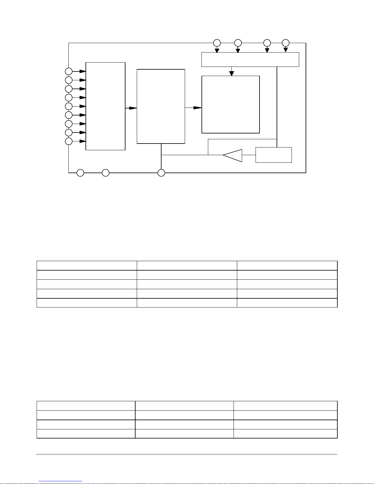
CH0
CH1
CH2
CH3
CH4
CH5
CH6
CH7
COM
A1
NCD9830
1
2
3
4
5
6
7
8
11
V
DD
Analog
MUX
GND
8-bit
A-to-D
Converter
1016 9
REFIN/REFOUT
Data Storage
A0
I
Temporary
2
C Interface
SDA SCL
14151213
2.5 V Ref
Figure 2. Block Diagram of NCD9830
HOW TO USE THIS MANUAL
Analog Interface
Two 8 way terminal blocks J1 & J2 are provided for
analog channels. They provide access to the analog input
Table 1. PIN CONFIGURATION OF J1 & J2
Pin Number Signal Notes
J1.1−J1.7 (Odd) CH0−CH3
J1.2−J1.8 (Even) GND Each Channel has Individual Ground
J2.1−J2.7 (Odd) CH4−CH7
J2.2−J2.8 (Even) GND Each Channel has Individual Ground
The analog inputs can be applied to J1 & J2 odd pins
e.g. J1.1 for CH0, J2.3 for CH5 and so on according to the
table above (Each channel name is marked explicitly on the
PCB). Even pins from J1.2−J1.8 & J2.2−J2.8 can be used as
ground for individual input channels.
Reference Voltage
The NCD9830 internal DAC can be configured with an
externally supplied (50 mV to 5 V) reference or an
internally generated reference voltage of 2.5 V. However, t o
pins of the ADC. The pin configurations of J1&J2 are
explained in Table 1.
avail of the full dynamic range an external reference of 5 V
must be used while operating the device at 5 V supply
voltage. The internal 2.5 V reference voltage is sufficient for
full dynamic range while operating the device at 2.7 V.
Jumper J5 is provided to switch external reference
ON/OFF. An inserted jumper corresponds to ON position
while it’s OFF otherwise. A 4 way terminal block J3 is
provided to supply external supply voltage (when a supply
voltage other than 3.3 V is used) and external reference
voltage. The pin configuration of J3 is explained in Table 2.
Table 2. PIN CONFIGURATION OF J3
Pin Number Signal Notes
J3.1 External Supply
J3.3 External Reference
J3.2 & J3.4 GND Individual Ground Provided for Easy Access
http://onsemi.com
2
Page 3
NCD9830GEVB
Power Supply
NCD9830 can be operated at supply voltage range
between 2.7V & 5V. The liberty of supply voltage variation
must be used with appropriate reference voltage selection
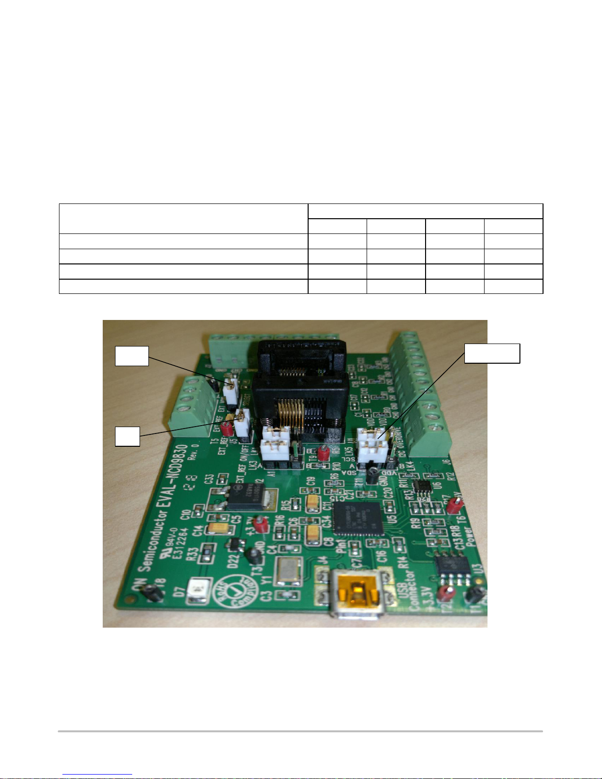
(see technical datasheet for more information). Link LK2 is
provided for appropriate supply voltage setting. Position B
corresponds to default value of 3.3V (internally generated)
while position A corresponds to externally supplied supply
voltage. The Board generates 3.3 V from the USB connector
provided. However, if any other operating voltage is
required then that must be supplied externally through J3.1
Table 3. LINKS POSITIONS SELECTION
Selection
3.3 V Supply Voltage with Internal Reference B A A OFF
3.3 V Supply Voltage with External Reference B A A ON
Externally Supplied Voltage with Internal Reference A B B OFF
Externally Supplied Voltage with External Reference A B B ON
and J3.3 as explained in Table 2. The digital interface of the
PCB is operated at 3.3 V. If NCD9830 supply voltage is
selected any value other than 3.3 V then appropriate
management of SCL and SDA signals is required to allow
proper I
2
C operation. Links LK4 & LK5 serve this purpose.
Position A corresponds to 3.3 V operation (default)
whereas, position B corresponds to all other externally
supplied voltages according to the technical datasheet.
A guide to proper selection of Links and jumper is shown in
Table 3.
Links Positions
LK2 LK4 LK5 J5
LK2
J5
LK4 & LK5
Figure 3. Photograph of PCB Side Showing J5, LK2, LK4 & LK5
http://onsemi.com
3
Page 4

NCD9830GEVB
Address Selection
Links LK1 & LK3 are provided for appropriate address
selection as explained in the technical data sheet. LK1
corresponds to A0 while LK3 corresponds to A1. Position A
Table 4. APPROPRIATE ADDRESS SELECTION
Address Selection
0x48 A A
0x49 A B
0x4A B A
0x4B B B
LK1 & LK3 for A0A1 Selection
corresponds to 0 (GND) while position B corresponds to 1
(VDD). The default position of these links is A0A1 = 00
which gives a hexadecimal address of 0x48.
Links Positions
LK1 LK3
Figure 4. Photograph of PCB Side Showing LK1 & LK3 (A0A1)
http://onsemi.com
4
Page 5
NCD9830GEVB
Digital Interface & Software
A USB cable is provided to interface the NCD9830 board
to computer. A software file NCD9830_REV5.exe along
with its associated .hex file is also provided. Save the .exe
This small green square shows that firmware is
downloaded successfully. If it is red check USB
connection and address settings.
file and the .hex file in the same folder for proper interfacing
of the device with the software. Double click the
NCD9830_REV5.exe file and the user graphical interface
window will open as shown in Figure 5 below.
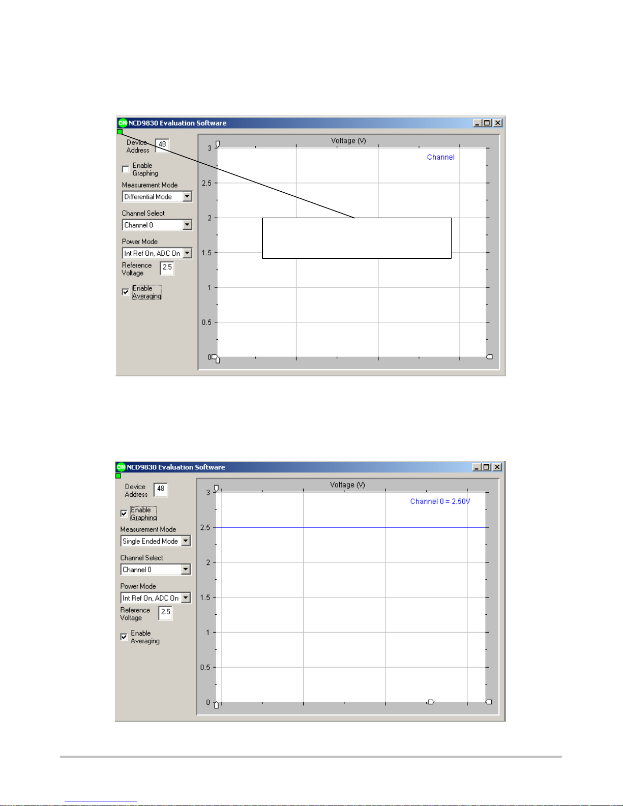
Figure 5. Graphical User Interface
Select “Measurement mode”, and “channel Select”
appropriately from drop down menu. The power mode
needs to b e a t “Int Ref On, ADC On” to allow operation with
internal reference. Check Enable Averaging for a better
averaged result of the output. Check Enable Graphing to see
the output value graphically as shown below in Figure 6.
Figure 6. Graphical User Interface Showing a Sample CH0 Output Value
http://onsemi.com
5
Page 6

NCD9830GEVB
EVALUATION BOARD SCHEMATIC
http://onsemi.com
6
Page 7

NCD9830GEVB
http://onsemi.com
7
Page 8

NCD9830GEVB
P
al
Table 5. BILL OF MATERIALS
Qty
1 Y1 Crystal SMD 24 MHz Abracorn Cooperation
1 U6 SN74LVC3G07DCTR Triple Buffer
1 U5 USB Microcontroller (CY7C68013A−56LTXC)
1 U1 NCD9830, 8 bit A/D Converter
1 U3 24LC64 64K I2C Serial EEPROM
1 U2 3.3 V Regulator NCP5501
1 U4 TSSOP16 Socket
5 T1, T3, T8, T10, T11 TERMINAL, PCB, BLACK, PK100 VERO
2 SCL−VDD, SDA−VDD TERMINAL, PCB, YELLOW, PK 100 VERO
6 T2, T4−7, T9 TERMINAL, PCB, RED, PK100 VERO
8 R0−4, R7−9, R16 Resistor 0R, 0603, 0.1W, 1%, CRCW06030000Z0EA Vishay
7 R11−13, R17−20
1 R16 Resistor 0R, 0603, 63 mW, 5%, Multicomp
1 R33
3 R5, R10, R14
2 R6, R15
1 J5 HEADER, 1ROW, 2WAY & JUMPER 2 PIN PCB
5 LK1−5 HEADER, 1ROW, 3WAY & JUMPER 2 PIN PCB
5 J1−3 TERMINAL BLOCK. PCB, 3.81MM, 4WAY Phoenix Contact
1 J4 USB Mini-B Receptacle Molex
1 J6 TERMINAL BLOCK, PCB, 3.81MM, 3WAY Phoenix Contact
1 D7 LED SMD GREEN OSRAM
1 D22 DIODE, SCHOTTKY, SOT−23
12 C1, C12, C17−18, C22−29 NOT POPULATED (Customer Selection)
4 C2, C11, C14, C31
2 C3−4 CAP 22 pF, 50 V, SMD Ceramic Capacitor Yageo
14 C5−7, C10, C13, C15−16,
1 C8
Reference Description
Resistor 3.3kW, 0603, 63 mW, 5%, Multicomp
Resistor 1kW, 0805, 100 mW, 1%, Multicomp
Resistor 10kW, 0603, 0.125 W, 1%, Multicomp
Resistor 100kW, 0603, 0.125, 1%, Multicomp
CAP 10 mF, 10 V SMD Tantalum Capacitor
CAPACITOR, 0603, 0.1 mF, 25V Multicomp
C19−21, C30, C32−34
CAP 2.2 mF, 10 V SMD Tantalum Capacitor
ON Semiconductor and the are registered trademarks of Semiconductor Components Industries, LLC (SCILLC) or its subsidiaries in the United States and/or other countries.
SCILLC owns the rights to a number of patents, trademarks, copyrights, trade secrets, and other intellectual property. A listing of SCILLC’s product/patent coverage may be accessed
at www.onsemi.com/site/pdf/ Patent− Marking.pdf . S CILLC reserves t he right to m ake changes wit hout further notice to any products h erein. SCILLC makes no warranty, representation
or guarantee regarding the suitability of its products for any particular purpose, nor does SCILLC assume any liability arising out of the application or use of any product or circuit, and
specifically disclaims any and all liability, including without limitation special, consequential or incidental damages. “Typical” parameters which may be provided in SCILLC data sheets
and/or specifications can and do vary in different applications and actual performance may vary over time. All operating parameters, including “Typicals” must be validated for each
customer application by customer’s technical e xperts. SCILLC does not convey any license u nder its patent rights nor the rights of others. SCILLC p roducts a re n ot d esigned, i ntended,
or authorized for use as components in systems intended for surgic al i mplant into the body, or other applications intended t o s upport o r s ust ain life, or for any other application in which
the failure of the SCILLC product could create a situation where personal injury or death may occur. Should Buyer purchase or use SCILLC products for any such unintended or
unauthorized application, Buyer shall indemnify and hold SCILLC and its officers, em ployees, subsidiaries, affiliates, and distributors harmless against all claims, costs, damages, and
expenses, and reasonable at torney f ees a r ising o ut o f, d irectly o r indirectly, any claim o f personal injury or death associated w ith s uch u nintended o r u nauthorized u se, e ven if such claim
alleges that SCILLC was negligent r egarding the design o r manuf acture o f t he p art. SCILLC is a n E qual O pportunity/Af firmative Ac tion Employer. This literature is subject to all a pplicable
copyright laws and is not for resale in any manner.
UBLICATION ORDERING INFORMATION
LITERATURE FULFILLMENT:
Literature Distribution Center for ON Semiconductor
P.O. Box 5163, Denver, Colorado 80217 USA
Phone: 303−675−2175 or 800−344−3860 Toll Free USA/Canada
Fax: 303−675−2176 or 800−344−3867 Toll Free USA/Canada
Email: orderlit@onsemi.com
N. American Technical Support: 800−282−9855 Toll Free
USA/Canada
Europe, Middle East and Africa Technical Support:
Phone: 421 33 790 2910
Japan Customer Focus Center
Phone: 81−3−5817−1050
http://onsemi.com
8
ON Semiconductor Website: www.onsemi.com
Order Literature: http://www.onsemi.com/orderlit
For additional information, please contact your loc
Sales Representative
EVBUM2270/D
 Loading...