

NCD57090A,NCV57090A,NCD57091A,NCV57091A,NCD57090B,NCV57090B,NCD57091B,NCV57091B,NCD57090C,NCV57090C,NCD57091C,NCV57091C,NCD57090D,NCV57090D,NCD57091D,NCV57091D,NCD57090E,NCV57090E,NCD57091E,NCV57091E,NCD57090F,NCV57090F,NCD57091F,NCV57091F
ON Semiconductor NCD57090A,NCV57090A,NCD57091A,NCV57091A,NCD57090B,NCV57090B,NCD57091B,NCV57091B,NCD57090C,NCV57090C,NCD57091C,NCV57091C,NCD57090D,NCV57090D,NCD57091D,NCV57091D,NCD57090E,NCV57090E,NCD57091E,NCV57091E,NCD57090F,NCV57090F,NCD57091F,NCV57091F User Manual
Page 1
Isolated High Current
IGBT/MOSFET Gate Driver
NCx57090y, NCx57091y
(x = D or V, y = A, B, C, D, E or F)
NCx57090y, NCx57091y are high−current single channel
IGBT/MOSFET gate drivers with 5 kVrms internal galvanic isolation,
designed for high system efficiency and reliability in high power
applications. The devices accept complementary inputs and depending
on the pin configuration, offer options such as Active Miller Clamp
(version A/D/F), negative power supply (version B) and separate high
and low (OUTH and OUTL) driver outputs (version C/E) for system
design convenience. The driver accommodate wide range of input
bias voltage and signal levels from 3.3 V to 20 V and they are
available in wide−body SOIC−8 package.
Features
• High Peak Output Current (+6.5 A/−6.5 A)
• Low Clamp Voltage Drop Eliminates the Need of Negative Power
Supply to Prevent Spurious Gate Turn−on (Version A/D/F)
• Short Propagation Delays with Accurate Matching
• IGBT/MOSFET Gate Clamping during Short Circuit
• IGBT/MOSFET Gate Active Pull Down
• Tight UVLO Thresholds for Bias Flexibility
• Wide Bias Voltage Range including Negative V
• 3.3 V, 5 V, and 15 V Logic Input
• 5 kVrms Galvanic Isolation
• High Transient Immunity
• High Electromagnetic Immunity
• NCV Prefix for Automotive and Other Applications Requiring
Unique Site and Control Change Requirements; AEC−Q100
Qualified and PPAP Capable
• These Devices are Pb−Free, Halogen Free/BFR Free and are RoHS
Compliant
Typical Applications
• Motor Control
• Uninterruptible Power Supplies (UPS)
• Automotive Applications
• Industrial Power Supplies
• Solar Inverters
(Version B)
EE2
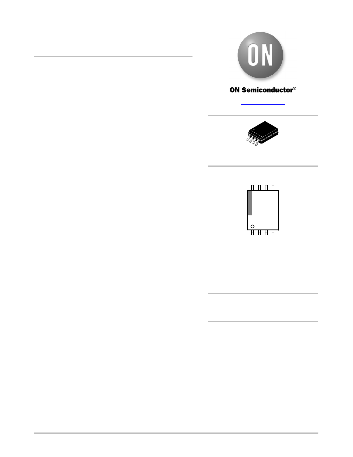
www.onsemi.com
SOIC8 WB
CASE 751EW
MARKING DIAGRAM
8
5709zy
ALYW
G
1
5709zy = Specific Device Code
z = 0/1
y = A/B/C/D/E/F
A = Assembly Location
L = Wafer Lot
Y = Year
W = Work Week
G = Pb−Free Package
PIN CONNECTIONS
See detailed pin connection information on page 2 of this
data sheet.
ORDERING INFORMATION
See detailed ordering and shipping information on page 23 of
this data sheet.
© Semiconductor Components Industries, LLC, 2019
April, 2021 − Rev. 0
1 Publication Order Number:
NCD57090A/D
Page 2
NCx57090y, NCx57091y
PIN CONNECTIONS
V
DD1
IN+
IN−
GND1
GND2
CLAMP
OUT
V
DD2
V
DD1
IN+
IN−
GND1
NCx57090A, NCx57091A NCx57090B, NCx57091B
V
DD1
IN+
IN−
GND1
NCx57090D
CLAMP
OUT
V
DD2
GND2
V
DD1
IN+
IN−
GND1
NCx57090E
NOTE: x = D or V
Figure 1. Pin Connections
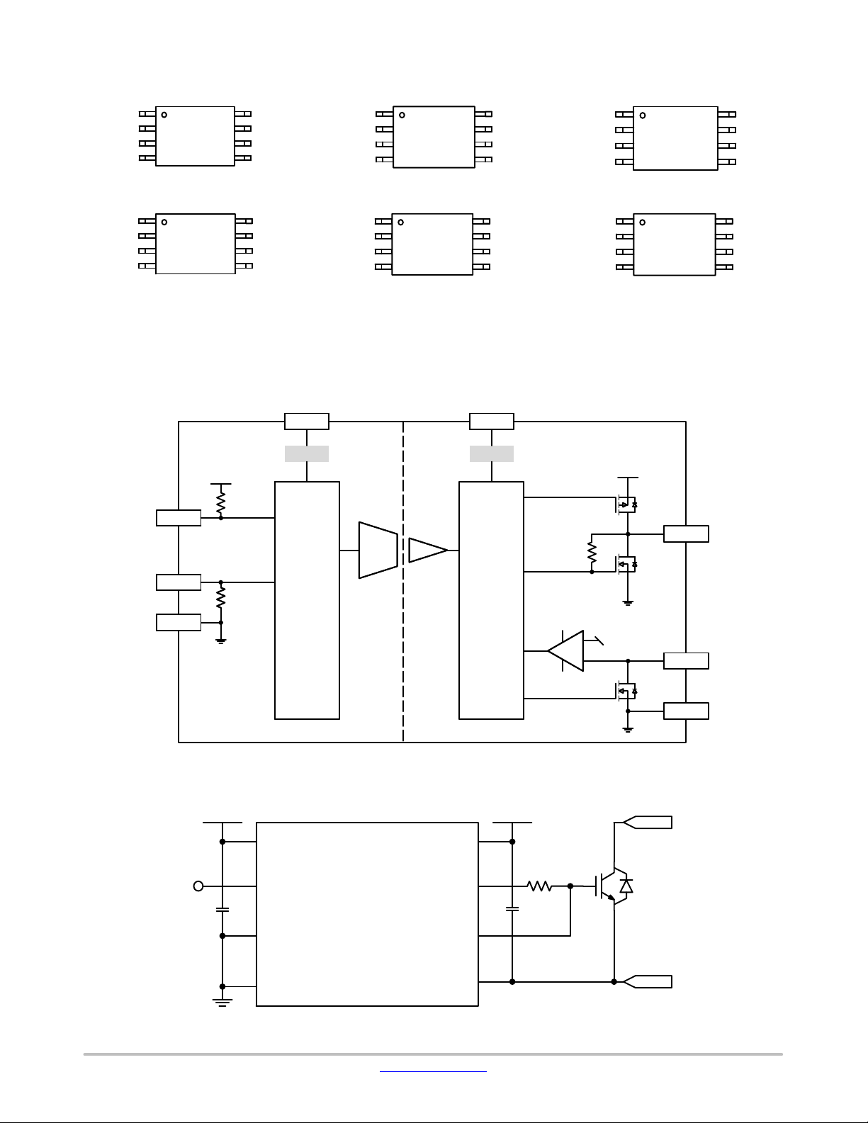
BLOCK DIAGRAM AND APPLICATION SCHEMATIC − VERSION A/D/F
V
DD1
UVLO1
V
DD1
IN−
V
GND2
OUT
V
OUTL
OUTH
V
GND2
V
DD2
UVLO2
EE2
DD2
DD2
V
DD1
IN+
IN−
GND1
NCx57090C, NCx57091C
V
DD1
IN+
IN−
GND1
NCx57090F
V
DD2
OUT
GND2
OUTL
OUTH
V
DD2
V
DD2
OUT
CLAMP
GND2
IN+
GND1
Logic
1
Logic
+
−
V
CLAMP−THR
2
CLAMP
GND2
2
Figure 2. Simplified Block Diagram, NCD57090A/D/F
V
DD1
V
DD1
V
DD2
OUTIN+
IN−
GND1
CLAMP
GND2
V
DD2
Figure 3. Simplified Application Schematics, Version A/D/F
www.onsemi.com
2
Page 3
NCx57090y, NCx57091y
BLOCK DIAGRAM AND APPLICATION SCHEMATIC − NCx57090B, NCx57091B
IN−
IN+
GND1
V
DD1
V
DD2
UVLO2UVLO1
V
V
DD1
DD2
OUT
Logic
Logic
V
EE2
1
GND2
2
Figure 4. Simplified Block Diagram, NCx57090B, NCx57091B
V
DD1
V
DD2
V
V
DD1
DD2
OUTIN+
IN−
GND1
GND2
V
EE2
Figure 5. Simplified Application Schematics, NCx57090B, NCx57091B
www.onsemi.com
3
Page 4
NCx57090y, NCx57091y
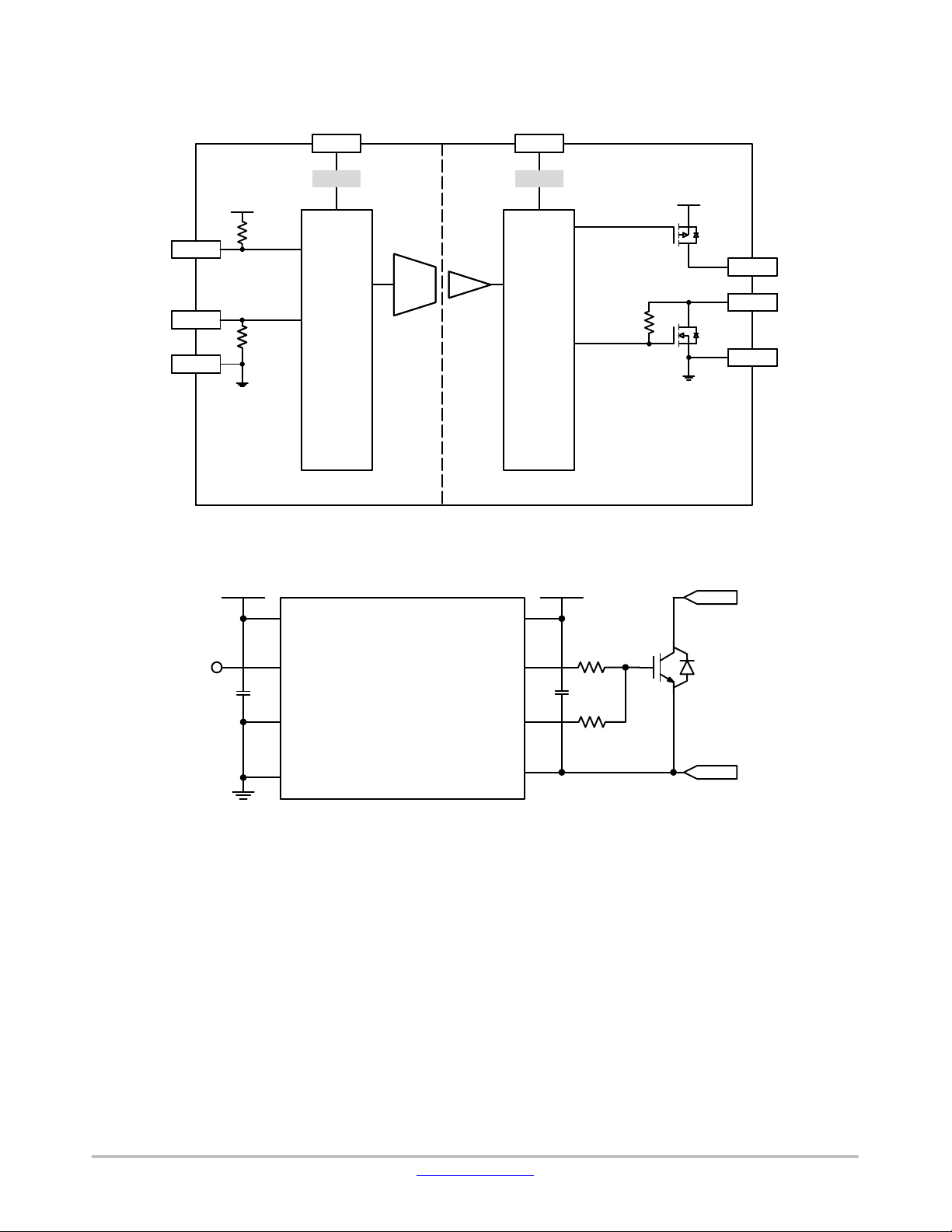
BLOCK DIAGRAM AND APPLICATION SCHEMATIC − VERSION C/E
IN−
IN+
GND1
V
DD1
V
DD2
UVLO2UVLO1
V
V
DD1
DD2
OUTH
OUTL
Logic
Logic
GND2
1
2
Figure 6. Simplified Block Diagram, Version C/E
V
DD1
V
DD2
V
V
DD1
DD2
OUTHIN+
IN−
GND1
OUTL
GND2
Figure 7. Simplified Application Schematics, Version C/E
www.onsemi.com
4
Page 5
NCx57090y, NCx57091y
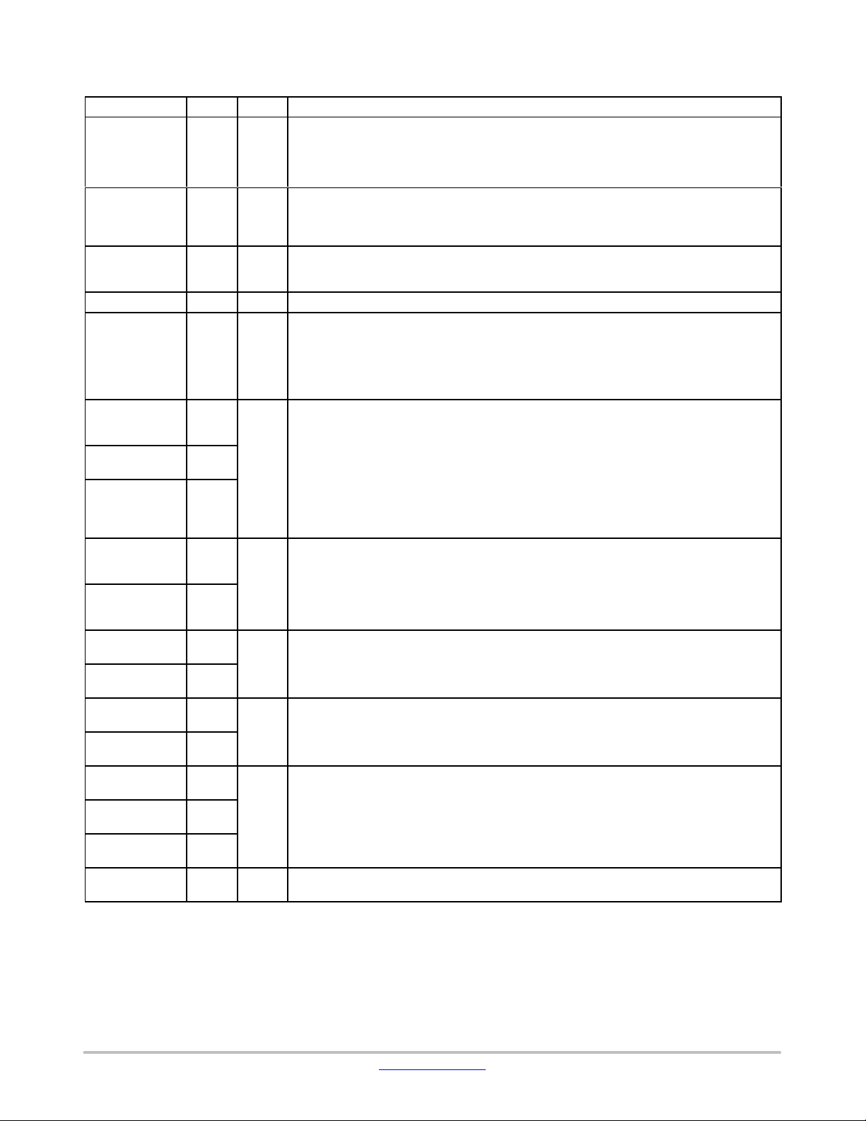
Table 1. FUNCTION DESCRIPTION
Pin Name No. I/O Description
V
DD1
IN+ 2 I Non inverted gate driver input. It is internally clamped to V
IN− 3 I Inverted gate driver input. It is internally clamped to V
GND1 4 Power Input side ground reference.
V
DD2
GND2
(NCD57090A,
NCD57090C)
GND2
(NCD57090B)
GND2
(NCD57090D,
NCD57090E,
NCD57090F)
OUT
(NCD57090A,
NCD57090B)
OUT
(NCD57090D,
NCD57090F)
OUTH
(NCD57090C)
OUTH
(NCD57090E)
OUTL
(NCD57090C)
OUTL
(NCD57090E)
CLAMP
(NCD57090A)
CLAMP
(NCD57090D)
CLAMP
(NCD57090F)
V
EE2
(NCD57090B)
1 Power Input side power supply. A good quality bypassing capacitor is required from this pin to GND1
and should be placed close to the pins for best results.
The under voltage lockout (UVLO) circuit enables the device to operate at power on when
a typical supply voltage higher than V
Please see Figures 9A and 9B for more details.
UVLO1−OUT−ON
pull−down resistor of 125 kW to ensure that output is low in the absence of an input signal.
A minimum positive or negative pulse−width is required at IN+ before OUT or OUTH/OUTL
responds.
resistor of 50 kW to ensure that output is low in the absence of an input signal. A minimum
positive or negative pulse−width is required at IN− before OUT or OUTH/OUTL responds.
5 Power Output side positive power supply. The operating range for this pin is from UVLO2 to its
maximum allowed value. A good quality bypassing capacitor is required from this pin to GND2
and should be placed close to the pins for best results.
The under voltage lockout (UVLO) circuit enables the device to operate at power on when
a typical supply voltage higher than V
for more details.
Power Output side gate drive reference connecting to IGBT emitter or MOSFET source.
8
UVLO2−OUT−ON
7
5
6
O Driver output that provides the appropriate drive voltage and source/sink current to the IGBT/
MOSFET gate. OUT is actively pulled low during start−up.
7
6
O Driver high output that provides the appropriate drive voltage and source current to the IGBT/
MOSFET gate.
7
7
O Driver low output that provides the appropriate drive voltage and sink current to the IGBT/
MOSFET gate. OUTL is actively pulled low during start−up.
8
7
O Provides clamping for the IGBT/MOSFET gate during the off period to protect it from parasitic
turn−on. Its internal N FET is turned on when the voltage of this pin falls below V
8
It is to be tied directly to IGBT/MOSFET gate with minimum trace length for best results.
6
8 Power Output side negative power supply. A good quality bypassing capacitor is required from this pin
to GND2 and should be placed close to the pins for best results.
is present.
and has an equivalent
DD1
and has an equivalent pull−up
DD1
is present. Please see Figure 9C and 9D
CLAMP−THR
.
www.onsemi.com
5
Page 6
NCx57090y, NCx57091y
Table 2. SAFETY AND INSULATION RATINGS
Symbol Parameter Value Unit
Installation Classifications per DIN VDE 0110/1.89
Table 1 Rated Mains
Voltage
CTI
Comparative Tracking Index (DIN IEC 112/VDE 0303 Part 1) 600
Climatic Classification 40/100/21
Pollution Degree (DIN VDE 0110/1.89) 2
V
V
V
V
E
PR
IORM
IOWM
IOTM
CR
E
Input−to−Output Test Voltage, Method b, V
100% Production Test with tm = 1 s, Partial Discharge < 5 pC
× 1.875 = VPR,
IORM
Maximum Repetitive Peak Voltage 1200 V
Maximum Working Voltage 870 V
Highest Allowable Over Voltage 8400 V
External Creepage 8.0 mm
External Clearance 8.0 mm
CL
DTI Insulation Thickness 17.3
T
Case
P
S,INPUT
P
S,OUTPUT
R
Safety Limit Values – Maximum Values in Failure; Case Temperature 150 °C
Safety Limit Values – Maximum Values in Failure; Input Power 121 mW
Safety Limit Values – Maximum Values in Failure; Output Power 1349 mW
Insulation Resistance at TS, VIO = 500 V 10
IO
< 150 V
< 300 V
< 450 V
< 600 V
< 1000 V
RMS
RMS
RMS
RMS
RMS
I − IV
I − IV
I − IV
I − IV
I − III
2250 V
9
pk
pk
RMS
pk
mm
W
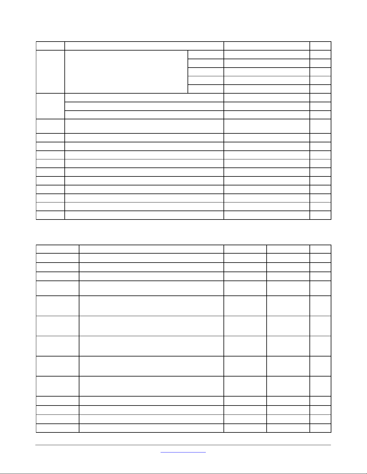
Table 3. ABSOLUTE MAXIMUM RATINGS (Note 1)
Over operating free−air temperature range unless otherwise noted.
Symbol
V
−GND1 Supply Voltage, Input Side −0.3 22 V
DD1
V
−GND2 Positive Power Supply, Output Side −0.3 32 V
DD2
V
−GND2 Negative Power Supply, Output Side −18 0.3 V
EE2
V
DD2−VEE2
(V
MAX2
)
Differential Power Supply, Output Side (NCD57090B) 0 36 V
Gate−driver Output High Voltage
V
V
OUTH
OUT
−GND2
−GND2
NCD57090A/B/D/F
NCD57090C/E
Gate−driver Output Low Voltage
V
−GND2
OUT
−GND2
V
OUTL
I
PK−SRC
I
PK−SNK
I
PK−CLAMP
t
CLP
V
−GND1 Voltage at IN+, IN− −0.3 V
LIM
V
−GND2 Clamp Voltage −0.3 V
CLAMP
P
D
NCD57090A/B/D/F
NCD57090C/E
Gate−driver Output Sourcing Current
(maximum pulse width = 10 ms, maximum duty cycle = 0.2%,
= 15 V, V
V
DD2
EE2
Gate−driver Output Sinking Current
(maximum pulse width = 10 ms, maximum duty cycle = 0.2%,
= 15 V, V
V
DD2
EE2
Clamp Sinking Current
(maximum pulse width = 10 ms, maximum duty cycle = 0.2%,
= 2.5 V)
V
CLAMP
Maximum Short Circuit Clamping Time (I
Power Dissipation (SOIC−8 Wide Package) − 1470 mW
Parameter Minimum Maximum Unit
−
−
V
DD2
−0.3
−
− 6.5 A
= 0 V)
− 6.5 A
= 0 V)
− 2.5 A
OUT_CLAMP
= 500 mA) − 10
DD1
DD2
+ 0.3
−
−
−
+ 0.3 V
+ 0.3 V
V
V
ms
www.onsemi.com
6
Page 7
NCx57090y, NCx57091y
Table 3. ABSOLUTE MAXIMUM RATINGS (Note 1) (continued)
Over operating free−air temperature range unless otherwise noted.
Symbol UnitMaximumMinimumParameter
TJ(max) Maximum Junction Temperature −40 150 °C
T
STG
ESDHBM ESD Capability, Human Body Model (Note 2) − ±2 kV
ESDCDM ESD Capability, Charged Device Model (Note 2) − ±2 kV
MSL Moisture Sensitivity Level − 1 −
T
SLD
Stresses exceeding those listed in the Maximum Ratings table may damage the device. If any of these limits are exceeded, device functionality
should not be assumed, damage may occur and reliability may be affected.
1. Refer to ELECTRICAL CHARACTERISTICS and APPLICATION INFORMATION for Safe Operating Area.
2. This device series incorporates ESD protection and is tested by the following methods:
ESD Human Body Model tested per AEC−Q100−002 (EIA/JESD22−A114).
ESD Charged Device Model tested per AEC−Q100−011 (EIA/JESD22−C101).
Latchup Current Maximum Rating: ≤ 100 mA per JEDEC standard: JESD78, 25°C.
3. For information, please refer to our Soldering and Mounting Techniques Reference Manual, SOLDERRM/D.
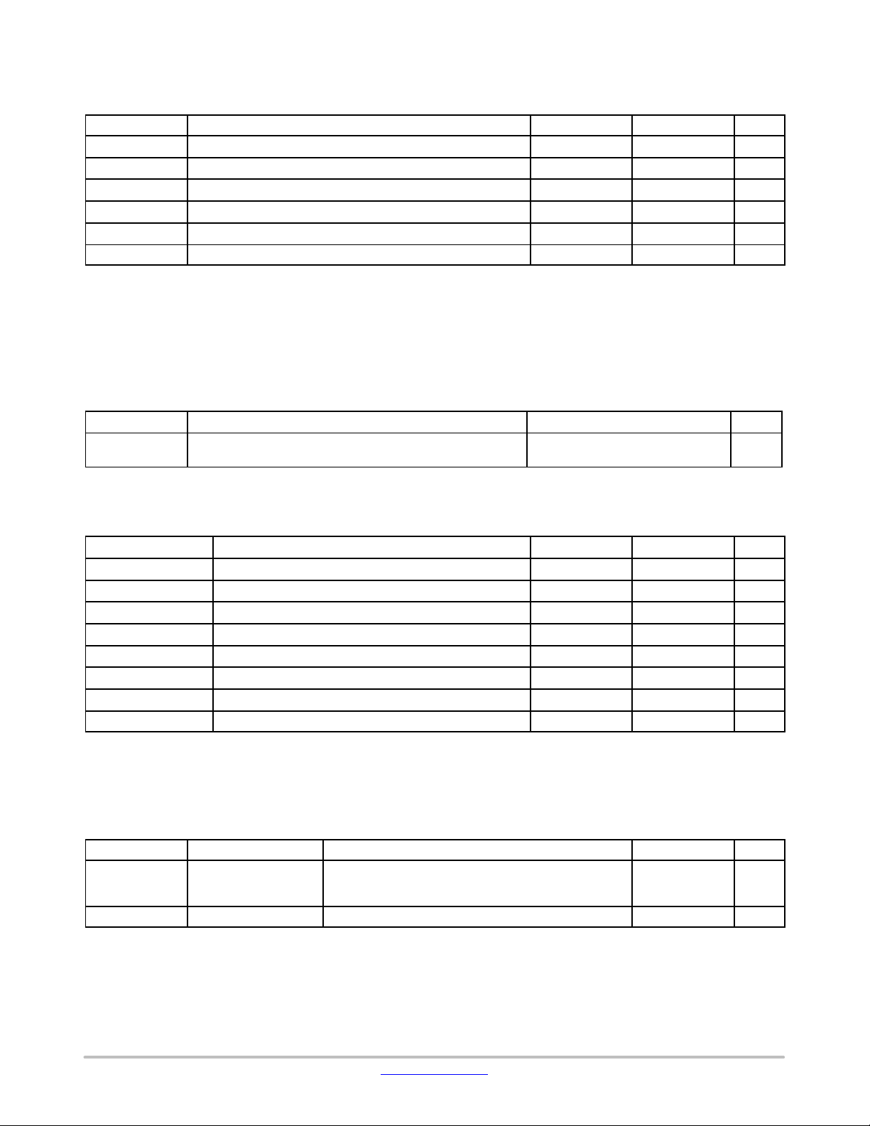
Table 4. THERMAL CHARACTERISTICS
Symbol Parameter Value Unit
RqJA Thermal Characteristics, SOIC−8 wide body (Note 4)
4. Refer to ELECTRICAL CHARACTERISTICS and APPLICATION INFORMATION for Safe Operating Area.
5. Values based on copper area of 100 mm
Storage Temperature Range −65 150 °C
Lead Temperature Soldering Reflow, Pb−Free (Note 3) − 260 °C
156 (1−Layer)
Thermal Resistance, Junction−to−Air (Note 5)
2
(or 0.16 in2) of 1 oz copper thickness and FR4 PCB substrate.
85 (4−Layer)
°C/W
Table 5. OPERATING RANGES (Note 6)
Symbol Parameter Min Max Unit
V
−GND1 Supply Voltage, Input Side UVLO1 20 V
DD1
V
−GND2 Positive Power Supply, Output Side UVLO2 30 V
DD2
V
−GND2 Negative Power Supply, Output Side (NCD57090B) −15 0 V
EE2
V
−VEE2 (V
DD2
|dV
V
V
ISO
IL
IH
) Differential Power Supply, Output Side (NCD57090B) 0 32 V
MAX2
Low Level Input Voltage at IN+, IN− (Note 7) 0 0.3 × V
High Level Input Voltage at IN+, IN− (Note 7) 0.7 × V
DD1
V
DD1
/dt| Common Mode Transient Immunity (Note 8) 100
DD1
V
V
kV/ms
TA Ambient Temperature −40 125 °C
Functional operation above the stresses listed in the Recommended Operating Ranges is not implied. Extended exposure to stresses beyond
the Recommended Operating Ranges limits may affect device reliability.
6. Refer to ELECTRICAL CHARACTERISTICS and APPLICATION INFORMATION for Safe Operating Area.
7. Table values are valid for 3.3 V and 5 V V
DD1, for higher VDD1 voltages, the threshold values are maintained at the 5 V VDD1 levels.
8. Was tested by ±1500 V pulses up to 100 kV/ms.
Table 6. ISOLATION CHARACTERISTICS
Symbol Parameter Conditions Value Unit
V
ISO, input−output
R
ISO
9. Device is considered a two−terminal device: pins 1 to 4 are shorted together and pins 5 to 9 are shorted together.
10.5,000 V
11. The input−output isolation voltage is a dielectric voltage rating per UL1577. It should not be regarded as an input−output continuous voltage
RMS
rating. For the continuous working voltage rating, refer to equipment−level safety specification or DIN VDE V 0884−11 Safety and Insulation
Ratings Table.
Input−Output Isolation
Voltage
TA = 25°C, Relative Humidity < 50%,
t = 1.0 minute, I
(Note 9, 10, 11)
Isolation Resistance V
= 500 V (Note 9) 10
I−O
for 1−minute duration is equivalent to 6,000 V
< 30 mA, 50 Hz
I−O
for 1−second duration.
RMS
5000 V
11
RMS
W
www.onsemi.com
7
Page 8
NCx57090y, NCx57091y
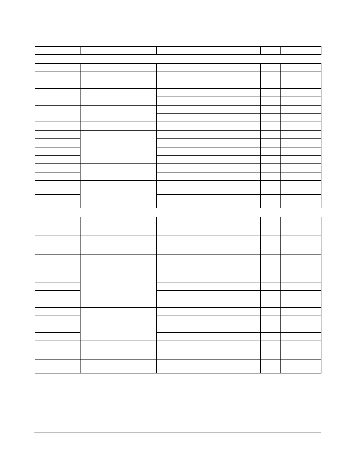
ELECTRICAL CHARACTERISTICS V
For typical values T
Symbol
VOLTAGE SUPPLY
V
UVLO1−OUT−ON
V
UVLO1−OUT−OFF
V
UVLO1−HYST
V
UVLO2−OUT−ON
V
UVLO2−OUT−OFF
V
UVLO2−HYST
I
DD1−0−3.3
I
DD1−0−5
I
DD1−0−15
I
DD1−100−5
I
DD2−0
I
DD2−100
I
EE2−0
I
EE2−100
LOGIC INPUT AND OUTPUT
V
IL
V
IH
V
IN−HYST
I
IN−L−3.3
I
IN−L−5
I
IN−L−15
I
IN−L−20
I
IN+H−3.3
I
IN+H−5
I
IN+H−15
I
IN+H−20
t
ON−MIN1
t
ON−MIN2
= 25°C, for min/max values, TA is the operating ambient temperature range that applies, unless otherwise noted.
A
Parameter Test Conditions Min Typ Max Unit
UVLO1 Output Enabled − − 3.1 V
UVLO1 Output Disabled 2.4 − − V
UVLO1 Hysteresis 0.1 − − V
UVLO2 Output Enabled
UVLO2 Output Disabled
UVLO2 Hysteresis 0.7 1 − V
Input Supply Quiescent Current
Output Positive Supply
Quiescent Current
Output Negative Supply
Quiescent Current (NCD57090B)
IN+, IN−, Low Input Voltage Level scale for V
IN+, IN−, High Input Voltage Level scale for V
Input Hysteresis Voltage Level scale for V
IN− Input Current
IN+ Input Current
Input Pulse Width of IN+, IN− for
Guaranteed No Response at
Output
Input Pulse Width of IN+, IN− for
Guaranteed Response at Output
DD1
= 5 V, V
= 15 V, (V
DD2
= 0 V for NCD57090B).
EE2
NCx57090y 12.4 12.9 13.4 V
NCx57091y 8.7 9 9.3 V
NCx57090y 11.5 12 12.5 V
NCx57091y 7.7 8 8.3 V
IN+ = Low, IN− = Low, V
= 3.3 V − − 2 mA
DD1
IN+ = Low, IN− = Low − − 2 mA
IN+ = Low, IN− = Low, V
= 15 V − − 2 mA
DD1
IN+ = High, IN− = Low − − 5.5 mA
IN+ = Low, IN− = Low, no load − − 2 mA
IN+ = High, IN− = Low, no load − − 2 mA
IN+ = Low, IN− = Low, no load,
V
= −8 V
EE2
IN+ = High, IN− = Low, no load, V
= −8 V
= 3.3 to 5 V
for V
> 5 V is the same as for
DDI
= 5 V
V
DDI
for V
> 5 V is the same as for
DDI
V
= 5 V
DDI
for V
> 5 V is the same as for
DDI
V
= 5 V
DDI
V
= 0 V, V
IN−
V
= 0 V − − 100
IN−
V
= 0 V, V
IN−
V
= 0 V, V
IN−
V
= V
IN+
V
= V
IN+
V
= V
IN+
V
= V
IN+
DDI
= 3.3 to 5 V
DDI
= 3.3 to 5 V
DDI
= 3.3 V − − 100
DD1
= 15 V − − 100
DD1
= 20 V − − 100
DD1
= 3.3 V − − 100
DD1
= 5 V − − 100
DD1
= 15 V − − 100
DD1
= 20 V − − 100
DD1
EE2
− − 2 mA
− − 2 mA
− − 0.3 ×
V
DD1
0.7 ×
V
DD1
− 0.15 ×
− − V
− V
V
DD1
− − 10 ns
40 − − ns
V
mA
mA
mA
mA
mA
mA
mA
mA
www.onsemi.com
8
Page 9

NCx57090y, NCx57091y
ELECTRICAL CHARACTERISTICS V
For typical values T
Symbol UnitMaxTypMinTest ConditionsParameter
DRIVER OUTPUT
V
OUTL1
V
OUTL2
V
OUTH1
V
OUTH2
I
PK−SNK1
I
PK−SRC1
MILLER CLAMP (NCD57090A)
V
CLAMP
V
CLAMP−THR
IGBT SHORT CIRCUIT CLAMPING
V
CLAMP−OUTH
V
CLAMP−OUTL
V
CLAMP−CLAMP
DYNAMIC CHARACTERISTIC
t
PD−ON−3.3
t
PD−ON−5
t
PD−ON−15
t
PD−ON−20
t
PD−OFF−3.3
t
PD−OFF−5
t
PD−OFF−15
t
PD−OFF−20
t
DISTORT
t
DISTORT_TOT
t
Rise Time (see Figure 8) C
RISE
= 25°C, for min/max values, TA is the operating ambient temperature range that applies, unless otherwise noted.
A
Output Low State
(V
– GND2 for
OUT
NCD57090A/D/F)
– V
(V
OUT
(V
OUTL
NCD57090C/E)
for NCD57090B)
EE2
– GND2 for
Output High State
(V
– V
– V
– V
OUT
OUT
OUTL
for
for NCD57090B)
for
DD2
NCD57090A/B/D/F)
(V
DD2
(V
DD2
NCD57090C/E)
Peak Driver Current, Sink
(Note 12)
Peak Driver Current, Source
(Note 12)
Clamp Voltage
Clamp Activation Threshold 1.5 2 2.5 V
Clamping Voltage, Sourcing
(V
/ V
OUTH
– V
DD2
OUT
Clamping Voltage, Sinking
(V
− V
OUTL
DD2
)
Clamping Voltage, Clamp
(V
(NCD57090A/D/F)
CLAMP
− V
DD2
)
IN+, IN− to Output High
Propagation Delay
IN+, IN− to Output Low
Propagation Delay
Propagation Delay Distortion
PD−ON
− t
PD−OFF
(= t
Prop Delay Distortion between
Parts
DD1
)
= 5 V, V
)
= 15 V, (V
DD2
I
= 200 mA − 0.15 0.3
SINK
I
= 1.0 A, TA = 25°C − − 0.8
SINK
I
= 200 mA − 0.2 0.35
SRC
I
= 1.0 A, TA = 25°C − − 1.0
SRC
= 0 V for NCD57090B).
EE2
− 6.5 − A
− 6.5 − A
I
= 2.5 A, TA = 25°C − 2 −
CLAMP
I
= 2.5 A,
CLAMP
T
= −40°C to 125°C
A
IN+ = Low, IN− = High,
I
CLAMP−OUT/OUTH
(pulse test, t
CLPmax
= 500 mA,
= 10 ms)
IN+ = High, IN− = Low,
I
CLAMP−OUTL
(pulse test, t
= 500 mA,
= 10 ms)
CLPmax
IN+ = High, IN− = Low,
I
CLAMP−CLAMP
(pulse test, t
C
LOAD
VIH to 10% of output change
CLPmax
= 10 nF
= 500 mA
= 10 ms)
− − 3.5
− 0.7 0.9 V
− 0.8 1.5 V
− 1.1 1.7 V
− − − −
Pulse Width > 150 ns.
V
= V
IN+
= V
IN+
= V
IN+
= V
IN+
= 10 nF
= V
IN+
= V
IN+
= V
IN+
= V
IN+
= 3.3V, V
= 5 V, V
= 15 V, V
= 20 V, V
= 3.3 V, V
= 5 V, V
= 15 V, V
= 20 V, V
DD1
V
DD1
V
DD1
V
DD1
C
LOAD
V
to 10% of output change
IH
Pulse Width > 150 ns.
V
DD1
V
DD1
V
DD1
V
DD1
= 0 V 40 60 90 ns
IN−
= 0 V 40 60 90 ns
IN−
= 0 V 40 60 90 ns
IN−
= 0 V 40 60 90 ns
IN−
− − − −
= 0 V 40 60 90 ns
IN−
= 0 V 40 60 90 ns
IN−
= 0 V 40 60 90 ns
IN−
= 0 V 40 60 90 ns
IN−
TA = 25°C, PW > 150 ns − 0 − ns
TA = −40°C to 125°C, PW > 150 ns −25 − 25 ns
PW > 150 ns −30 0 30 ns
= 1 nF,
LOAD
10% to 90% of Output Change
− 13 − ns
V
V
V
www.onsemi.com
9
Page 10

NCx57090y, NCx57091y
ELECTRICAL CHARACTERISTICS V
For typical values T
= 25°C, for min/max values, TA is the operating ambient temperature range that applies, unless otherwise noted.
A
DD1
= 5 V, V
= 15 V, (V
DD2
= 0 V for NCD57090B).
EE2
Symbol UnitMaxTypMinTest ConditionsParameter
DYNAMIC CHARACTERISTIC
t
FALL
t
UVF1
t
UVR1
t
UVF2
t
UVR2
Fall Time (see Figure 8) C
UVLO1 Fall Delay (Note 12) − 1500 − ns
UVLO1 Rise Delay (Note 12) − 770 − ns
UVLO2 Fall Delay (Note 12) − 1000 − ns
UVLO2 Rise Delay (Note 12) − 1000 − ns
= 1 nF,
LOAD
90% to 10% of Output Change
− 13 − ns
Product parametric performance is indicated in the Electrical Characteristics for the listed test conditions, unless otherwise noted. Product
performance may not be indicated by the Electrical Characteristics if operated under different conditions.
12.Values based on design and/or characterization.
www.onsemi.com
10
Page 11

IN+
NCx57090y, NCx57091y
V
IH
V
IL
t
ON−MIN2
t
PD−ON
OUT/OUTH
V
DD2
V
UVLO1−OUT−ON
V
UVLO1−OUT−OFF
V
DD1
t
RISE
t
FALL
90%
t
PD−OFF
10%
Figure 8. Propagation Delay, Rise and Fall time
V
UVLO1−HYST
t
UVR1
t
UVF1
t
UVR1
t
UVF1
t
ON−MIN1
t
ON−MIN1
t
UVR2
t
UVR1−spread
IN+
OUT/OUTH
Figure 9.
Output Ramp−up and Ramp−down Times during UVLO1
Figure 9A. UVLO1 and Associated Timing Waveforms
www.onsemi.com
11
Page 12

V
DD2
V
UVLO1−OUT−ON
V
UVLO1−OUT−OFF
V
DD1
IN+
t
UVR1
NCx57090y, NCx57091y
t
UVF1
t
UVF1
t
UVR1
t
UVR1
t
UVR1−spread
OUT/OUTH
V
DD1
V
UVLO2−OUT−ON
V
UVLO2−OUT−OFF
V
DD2
IN+
V
Glitch Filtering
DD1
Figure 9B. UVLO1 Waveforms Depicting V
V
UVLO2−HYST
t
UVR2
t
UVF2
t
UVR2
Glitch Filtering
DD1
t
UVF2
t
UVR2
t
UVR2−spread
OUT/OUTH
Output Ramp−up and Ramp−down Times during UVLO2
Figure 9C. UVLO2 and Associated Timing Waveforms
www.onsemi.com
12
Page 13

V
DD1
V
UVLO2−OUT−ON
V
UVLO2−OUT−OFF
V
DD2
IN+
t
UVR2
NCx57090y, NCx57091y
t
UVF2
t
UVR2
t
UVR2
t
UVR2
t
UVR2−spread
OUT/OUTH
V
Glitch Filtering
DD2
Figure 9D. UVLO2 Waveforms Depicting V
V
DD1
IN+
IN−
V
DD1
Clamping
Circuit
V
DD1
Clamping
Circuit
Figure 10. Input Pin Structure
Glitch Filtering
DD2
www.onsemi.com
13
Page 14

NCx57090y, NCx57091y
TYPICAL CHARACTERISTICS
6
(3)
5
4
(2)
3
(1)
2
Current [mA]
1
0
−40 −20 0 20 40 60 100 120
80
Temperature [°C]
(1) I
DD1−0−3.3
(2) I
DD1−50−3.3
(3) I
DD1−100−3.3
Figure 11. I
, IN+ = 3.3 V/200 kHz/50%
Supply Current V
DD1
DD1
5
(3)
4
3
(2)
2
Current [mA]
(1)
1
= 3.3 V
5
(3)
4
3
(2)
2
Current [mA]
(1)
1
0
−40 −20 0 20 40 60 100 12080
Temperature [°C]
(1) I
DD1−0−5
(2) I
DD1−50−5
(3) I
DD1−100−5
Figure 12. I
, IN+ = 5 V/200 kHz/50%
Supply Current V
DD1
20
15
10
Current [mA]
5
= 5 V
DD1
(2)(3)
(1)
0
−40 −20 0 20 40 60 100 12080
Temperature [°C]
(1) I
DD1−0−20
(2) I
DD1−50−20
(3) I
DD1−100−20
Figure 13. I
, IN+ = 20 V/200 kHz/50%
Supply Current V
DD1
2.5
2
1.5
(2)
1
Current [mA]
0.5
(1)
0
−40 −20 0 20 40 60 100 12080
Temperature [°C]
(1) I
DD2−0−15
(2) I
DD2−100−15
Figure 15. I
Supply Current V
DD2
0
1 10 100 1000
= 20 V Figure 14. I
DD1
2.5
(2)
2
1.5
1
Current [mA]
(1)
0.5
0
−40 −20 0 20 40 60 100 12080
DD2
= 15 V
Figure 16. I
(1) CG = 1 nF
(2) CG = 10 nF
(3) CG = 100 nF
DD2
Temperature [°C]
(1) I
DD2−0−30
(2) I
DD2−100−30
Supply Current V
DD2
Frequency [kHz]
vs. Switching Frequency
= 30 V
DD2
www.onsemi.com
14
Page 15

NCx57090y, NCx57091y
TYPICAL CHARACTERISTICS (continued)
2.9
2.8
(1)
Voltage [V]
2.7
(2)
2.6
−40 −20 0 20 40 60 100 12080
Temperature [°C]
(1) V
UVLO1−OUT−ON
(2) V
UVLO1−OUT−OFF
Figure 17. UVLO1 Threshold Voltage
3
2.5
2
Voltage [V]
1.5
1.5
1.4
(2)
1.3
1.2
1.1
Voltage [V]
(1)
1
0.9
0.8
−40 −20 0 20 40 60 100 12080
Temperature [°C]
(1) V
CLAMP−OUTH
(2) V
CLAMP−CLAMP
Figure 18. IGBT Short Circuit CLAMP
Voltage Drop
2.00
1.98
1.96
1.94
Voltage [V]
1.92
1
−40 −20 0 20 40 60 100 12080
Temperature [°C]
Figure 19a. Miller Clamp Voltage (2.5 A)
13.5
(1)
13
12.5
Voltage [V]
11.5
(2)
12
−40 −20 0 20 40 60 100 12080
Temperature [°C]
(1) V
UVLO2−OUT−ON
(2) V
UVLO2−OUT−OFF
Figure 20. NCx57090 UVLO2 Threshold Voltage
1.90
−40 −20 0 20 40 60 100 12080
Temperature [°C]
Figure 19b. Miller Clamp Activation
Voltage Threshold
9.5
(1)
9
8.5
Voltage [V]
(2)
8
7.5
−40 −20 0 20 40 60 100 12080
Temperature [°C]
(1) V
UVLO2−OUT−ON
(2) V
UVLO2−OUT−OFF
Figure 21. NCx57091 UVLO2 Threshold Voltage
www.onsemi.com
15
Page 16

72
70
NCx57090y, NCx57091y
TYPICAL CHARACTERISTICS (continued)
71
68
(2)
66
Time [ns]
64
(1)
62
−40 −20 0 20 40 60 100 12080
Temperature [°C]
(1) t
(2) t
PD−ON−5
PD−ON−5
, IN+
, IN−
Figure 22. Propagation Delay Turn−on Figure 23. Propagation Delay Turn−off
15
14
Time [ns]
13
(1)
(2)
12
−40 −20 0 20 40 60 100 12080
Temperature [°C] Temperature [°C]
(1) t
, IN+
RISE
(2) t
, IN−
RISE
Figure 24. Rise Time, V
DD1
= 5 V
69
(1)
Time [ns]
67
(2)
65
−40 −20 0 20 40 60 100 12080
Temperature [°C]
(1) t
(2) t
PD−OFF−5
PD−OFF−5
, IN+
, IN−
14
13
Time [ns]
(1)
(2)
12
−40 −20 0 20 40 60 100 12080
(1) t
(2) t
FALL
FALL
, IN+
, IN−
Figure 25. Fall Time, V
DD1
= 5 V
50
40
(3)
(4)
Current [mA]
(2)
30
(1)
20
−40 −20 0 20 40 60 100 12080
Temperature [°C]
(1) I
IN+H−3.3
(2) I
IN+H−5
(3) I
IN+H−15
(4) I
IN+H−20
Figure 26. Input Current – Positive Input Figure 27. Input Current – Negative Input
−35
−35
−40
−45
Current [mA]
−50
−55
−60
www.onsemi.com
16
(1)
(2)
(3)(4)
−40 −20 0 20 40 60 100 12080
(1) I
IN−L−3.3
(2) I
IN−L−5
(3) I
IN−L−15
(4) I
IN−L−20
Page 17

NCx57090y, NCx57091y
Under Voltage Lockout (Refer to Figure 9x)
UVLO ensures correct switching of IGBT/MOSFET
connected to the driver output.
• The IGBT/MOSFET is turned−off and the output is
disabled if the supply V
V
UVLO1−OUT−OFF
V
UVLO2−OUT−OFF
or V
.
drops below
DD1
drops below
DD2
• The driver output does not follow the input signal on
IN+ or IN− until the V
V
UVLOX−OUT−ON
and the input signal rising edge is
applied to the IN+ or IN−
• V
is not monitored (NCx5709zB)
EE2
With high loading gate capacitances over 10 nF it is
important to follow the decoupling capacitor routing
guidelines as shown on Figure 35/36. The decoupling
capacitor value should be at least 10 mF. Also gate resistor
rises above the
DDX
of minimal value of 2 W has to be used in order to avoid
interference of the high di/dt with internal circuitry (e.g.
UVLO2).
After the power−on of the driver there has to be a rising
edge applied to the IN+ or falling edge to the IN− in order
for the output to start following the inputs. This serves as a
protection against producing partial pulses at the output if
the V
DD1
or V
is applied in the middle of the input PWM
DD2
pulse.
If the V
will appear on the output after t
t
UVR2−spread
end of t
rises over V
DD2
UVLO2−OUT−ON
UVR2
level the PWM
+ t
UVR2−spread
time is variable and is defined as a time from
to first rising edge on IN+ input. If the V
UVR2
. The
DD2
is starting from 0 V the time until PWM is at the output of
the driver is longer than t
UVR2
+ t
UVR2−spread
. This is caused
by start up time of internal circuits of the driver.
www.onsemi.com
17
Page 18

NCx57090y, NCx57091y
ACTIVE MILER CLAMP PROTECTION (CLAMP)
NCx5709yB supports bipolar power supply to prevent
unintentional turning on.
For operation with bipolar supplies, the IGBT/MOSFET
is turned off with a negative voltage through OUT with
respect to its emitter. This prevents the IGBT/MOSFET
from unintentionally turning on because of current induced
from its collector to its gate due to Miller effect. Typical
values for bipolar operation are V
= 15 V and V
DD2
EE2
= −5
V with respect to GND2.
Driver version A/D/F supports unipolar power supply
with active Miller clamp.
OUT/OUTH
For operation with unipolar supply, typically,
V
= 15 V with respect to GND2, and V
DD2
= GND2. In
EE2
this case, the IGBT/MOSFET can turn on due to additional
charge from IGBT/MOSFET Miller capacitance caused by
a high voltage slew rate transition on the IGBT collector/
MOSFET drain. To prevent IGBT/MOSFET to turn on, the
CLAMP pin is connected directly to IGBT/MOSFET gate
and Miller current is sinked through a low impedance
CLAMP transistor. When the IGBT/MOSFET is turned−off
and the gate voltage transitions below V
CLAMP
, the CLAMP
output is activated.
OUT/OUTH
Figure 28. Current Path with Miler Clamp Protection Figure 29. Current Path without Miler Clamp Protection
Non−inverting and Inverting Input Pin (IN+, IN−)
The driver has two possible input modes to control
IGBT/MOSFET. Both inputs have defined minimum input
pulse width to filter occasional glitches.
• Non−inverting input IN+ controls the driver output
while inverting input IN− is set to LOW
• Inverting input IN− controls the driver output while
WARNING: When the application uses an independent
or separate power supply for the control
unit and the input side of the driver, all
inputs should be protected by a serial
resistor (In case of a power failure of the
driver, the driver may be damaged due to
overloading of the input protection circuits)
non−inverting input IN+ is set to HIGH
www.onsemi.com
18
Page 19

NCx57090y, NCx57091y
Power Supply (V
DD1
, V
DD2
, V
EE2
)
The driver variant A/C/D/E and F are designed to support
unipolar power supply.
The driver variant B is designed to support bipolar power
supply.
Suitable external power capacitors are required for
reliable driving of IGBT/MOSFET gate with high current.
Parallel combination of 100 nF + 4.7 mF low ESR ceramic
capacitors is optimal for a wide range of applications using
IGBT/MOSFET. For reliable driving of IGBT modules
(containing several parallel IGBT’s) with a gate capacitance
over 10 nF a higher decoupling capacity is required
(typically 100 nF + 10 mF). Capacitors should be as close as
possible to the driver’s power pins. The recommended
layout is provided in the Figure 35 and 36.
V
DD1
IN+
IN−
GND1
Figure 30. Bipolar Power Supply (Variant B)
+
−
V
DD1
100nF
10
mF
• In bipolar power supply the driver is typically supplied
with a positive voltage of 15 V at V
voltage −5 V at V
(Figure 30). Negative power supply
EE2
prevents a dynamic turn on through the internal
IGBT/MOSFET input capacitance
DD2
• In Unipolar power supply the driver is typically supplied
with a positive voltage of 15 V at V
turn−on caused by the internal IGBT/MOSFET Miller
capacitance could be prevented by Active Miler Clamp
function (variant A/D/F). CLAMP output should be
directly connected to IGBT/MOSFET gate (Figure 28)
V
EE2
GND2
OUT
V
DD2
10
mF
100nF
10
mF
100nF
V
DD2
+
−
V
EE2
−
+
and negative
. Unwanted
DD2
V
DD1
V
DD1
+
−
100nF
10
mF
IN+
IN−
GND1
GND2
CLAMP
OUT
V
DD2
10
mF
100nF
V
DD2
+
−
Figure 31. Unipolar Power Supply (Variant A/D/F)
V
DD1
V
DD1
+
−
100nF
10
mF
IN+
IN−
GND1
GND2
OUTL
OUTH
V
DD2
10
mF
100nF
V
DD2
+
−
Figure 32. Unipolar Power Supply (Variant C/E)
www.onsemi.com
19
Page 20

Common Mode Transient Immunity (CMTI)
10μF
5V
+
-
FLOATING
5V
+
-
FLOATING
+
S1
-
10μF
+
S1
-
NCx57090y, NCx57091y
VDD1
IN+
IN-
GND1
HV PULSE
VDD1
IN+
IN-
GND1
HV PULSE
GND2
CLAMP
OUT
VDD2
GND2
OUTL
OUTH
VDD2
OUT must remain stable
OUT must remain stable
10μF
10μF
15V
15V
+
-
+
-
5V
+
-
FLOATING
10μF
+
S1
-
VDD1
IN+
IN-
GND1
HV PULSE
VEE2
GND2
OUT
VDD2
OUT must remain stable
10μF
Figure 33. Common−Mode Transient Immunity Test Circuit
High-speed signals
10 mils
0.25 mm
40 mils
1mm
10 mils
0.25 mm
Keep this space free
10 mils
from traces, pads and
0.25 mm
vias
10 mils
0.25 mm
40 mils
1mm
10 mils
0.25 mm
Ground plane
Power plane
Low-speed signals
314 mils
(8 mm)
Figure 34. Recommended Layer Stack
15V
+
-
www.onsemi.com
20
Page 21

NCx57090y, NCx57091y
Figure 35. Recommended Layout for Version A/B/C
www.onsemi.com
21
Page 22

NCx57090y, NCx57091y
Figure 36. Recommended Layout for Version D/E/F
www.onsemi.com
22
Page 23

ORDERING INFORMATION
Device Package Shipping
NCD57090ADWR2G
NCD57090BDWR2G
NCD57090CDWR2G
NCD57090DDWR2G
NCD57090EDWR2G
NCD57090FDWR2G
NCx57090y, NCx57091y
SOIC−8 Wide Body
(Pb−Free)
†
2500 / Tape & Reel
NCV57090ADWR2G*
NCV57090BDWR2G*
NCV57090CDWR2G*
NCV57090DDWR2G*
NCV57090EDWR2G*
NCV57090FDWR2G*
NCD57091ADWR2G (In Development)
NCD57091BDWR2G (In Development)
NCD57091CDWR2G (In Development)
NCV57091ADWR2G* (In Development)
NCV57091BDWR2G* (In Development)
NCV57091CDWR2G* (In Development)
†For information on tape and reel specifications, including part orientation and tape sizes, please refer to our Tape and Reel Packaging
Specifications Brochure, BRD8011/D.
*NCV Prefix for Automotive and Other Applications Requiring Unique Site and Control Change Requirements; AEC−Q100 Qualified and PPAP
Capable.
SOIC−8 Wide Body
(Pb−Free)
SOIC−8 Wide Body
(Pb−Free)
SOIC−8 Wide Body
(Pb−Free)
2500 / Tape & Reel
2500 / Tape & Reel
2500 / Tape & Reel
www.onsemi.com
23
Page 24

NCx57090y, NCx57091y
PACKAGE DIMENSIONS
SOIC8 WB
CASE 751EW
ISSUE A
q
q
www.onsemi.com
24
Page 25

NCx57090y, NCx57091y
ON Semiconductor and are trademarks of Semiconductor Components Industries, LLC dba ON Semiconductor or its subsidiaries in the United States and/or other countries.
ON Semiconductor owns the rights to a number of patents, trademarks, copyrights, trade secrets, and other intellectual property. A listing of ON Semiconductor’s product/patent
coverage may be accessed at www.onsemi.com/site/pdf/Patent−Marking.pdf
ON Semiconductor makes no warranty, representation or guarantee regarding the suitability of its products for any particular purpose, nor does ON Semiconductor assume any liability
arising out of the application or use of any product or circuit, and specifically disclaims any and all liability, including without limitation special, consequential or incidental damages.
Buyer is responsible for its products and applications using ON Semiconductor products, including compliance with all laws, regulations and safety requirements or standards,
regardless of any support or applications information provided by ON Semiconductor. “Typical” parameters which may be provided in ON Semiconductor data sheets and/or
specifications can and do vary in different applications and actual performance may vary over time. All operating parameters, including “Typicals” must be validated for each customer
application by customer’s technical experts. ON Semiconductor does not convey any license under its patent rights nor the rights of others. ON Semiconductor products are not
designed, intended, or authorized for use as a critical component in life support systems or any FDA Class 3 medical devices or medical devices with a same or similar classification
in a foreign jurisdiction or any devices intended for implantation in the human body. Should Buyer purchase or use ON Semiconductor products for any such unintended or unauthorized
application, Buyer shall indemnify and hold ON Semiconductor and its officers, employees, subsidiaries, affiliates, and distributors harmless against all claims, costs, damages, and
expenses, and reasonable attorney fees arising out of, directly or indirectly, any claim of personal injury or death associated with such unintended or unauthorized use, even if such
claim alleges that ON Semiconductor was negligent regarding the design or manufacture of the part. ON Semiconductor is an Equal Opportunity/Affirmative Action Employer. This
literature is subject to all applicable copyright laws and is not for resale in any manner.
. ON Semiconductor reserves the right to make changes without further notice to any products herein.
PUBLICATION ORDERING INFORMATION
LITERATURE FULFILLMENT:
Email Requests to: orderlit@onsemi.com
ON Semiconductor Website: www.onsemi.com
◊
TECHNICAL SUPPORT
North American Technical Support:
Voice Mail: 1 800−282−9855 Toll Free USA/Canada
Phone: 011 421 33 790 2910
www.onsemi.com
Europe, Middle East and Africa Technical Support:
Phone: 00421 33 790 2910
For additional information, please contact your local Sales Representative
25
 Loading...