

Page 1
NCD5703A, NCD5703B,
NCD5703C
High Current IGBT Gate
Drivers
The NCD5703A, NCD5703B and NCD5703C are high−current,
high−performance stand−alone IGBT drivers for high power
applications that include solar inverters, motor control and
uninterruptible power supplies. The devices offer a cost−effective
solution by eliminating external output buffer. Devices protection
features include accurate Under−voltage−lockout (UVLO),
desaturation protection (DESAT) and Active open−drain FAULT
output. The drivers also feature an accurate 5.0 V output. The drivers
are designed to accommodate a wide voltage range of bias supplies
including unipolar and NCD5703B even bipolar voltages.
Depending on the pin configuration the devices also include Active
Miller Clamp (NCD5703A) and separate high and low (V
driver outputs for system design convenience (NCD5703C).
All three available pin configuration variants have 8−pin SOIC
package.
Features
• High Current Output (+4/−6 A) at IGBT Miller Plateau voltages
• Low Output Impedance for Enhanced IGBT Driving
• Short Propagation Delay with Accurate Matching
• Direct Interface to Digital Isolator/Opto−coupler/Pulse Transformer
for Isolated Drive, Logic Compatibility for Non−isolated Drive
• DESAT Protection with Programmable Delay
• Tight UVLO Thresholds for Bias Flexibility
• Wide Bias Voltage Range
• This Device is Pb−Free, Halogen−Free and RoHS Compliant
NCD5703A Features
• Active Miller Clamp to Prevent Spurious Gate Turn−on
NCD5703B Features
• Negative Output Voltage for Enhanced IGBT Driving
NCD5703C Features
• Separate Outputs for V
OL
and V
OH
Typical Applications
• Solar Inverters
• Motor Control
• Uninterruptible Power Supplies (UPS)
• Rapid Shutdown for Photovoltaic Systems
and VOL)
OH
www.onsemi.com
MARKING
8
1
SOIC−8
D SUFFIX
CASE 751
NCD5703 = Specific Device Code
X = A, B or C
A = Assembly Location
L = Wafer Lot
Y = Year
W = Work Week
G = Pb−Free Package
DIAGRAM
8
NCD5703X
ALYW
G
1
PIN CONNECTIONS
VIN
VREF
FLT
DESAT
VIN
VREF
FLT
DESAT
VIN
VREF
FLT
DESAT
1
2
3
4
NCD5703A
1
2
3
4
NCD5703B
1
2
3
4
NCD5703C
8
7
6
5
8
7
6
5
8
7
6
5
CLAMP
GND
VO
VCC
VEE
GND
VO
VCC
GND
VOL
VOH
VCC
ORDERING INFORMATION
See detailed ordering and shipping information on page 9 of
this data sheet.
© Semiconductor Components Industries, LLC, 2018
August, 2019 − Rev. 1
1 Publication Order Number:
NCD5703/D
Page 2
NCD5703A, NCD5703B, NCD5703C
NCD5703A
DESAT
VREF
VCC
VIN
FLT
VCC
VO
CLAMP
GND
NCD5703B
VREF
VIN
FLT
DESAT
VCC
VO
GND
VEE
NCD5703C
VREF
VIN
DESAT
VCC
VOH
VOL
GND
VCC
VEE
VCC
FLT
Figure 1. Simplified Application Schematics
www.onsemi.com
2
Page 3
NCD5703A, NCD5703B, NCD5703C
FLT
DESAT
V
V
REF
V
SET
Q S
CLR
Q R
TSD
NCD5703A
I
DESAT-CHG
V
DESAT-THR
V
REF
IN
R
IN-
+
-
Bandgap
V
UVLO
-
CC
+
SET
S Q
CLR
R Q
DELAY
DELAY
-
+
V
MC-THR
SET
S Q
CLR
R Q
V
CC
V
O
CLAMP
GND
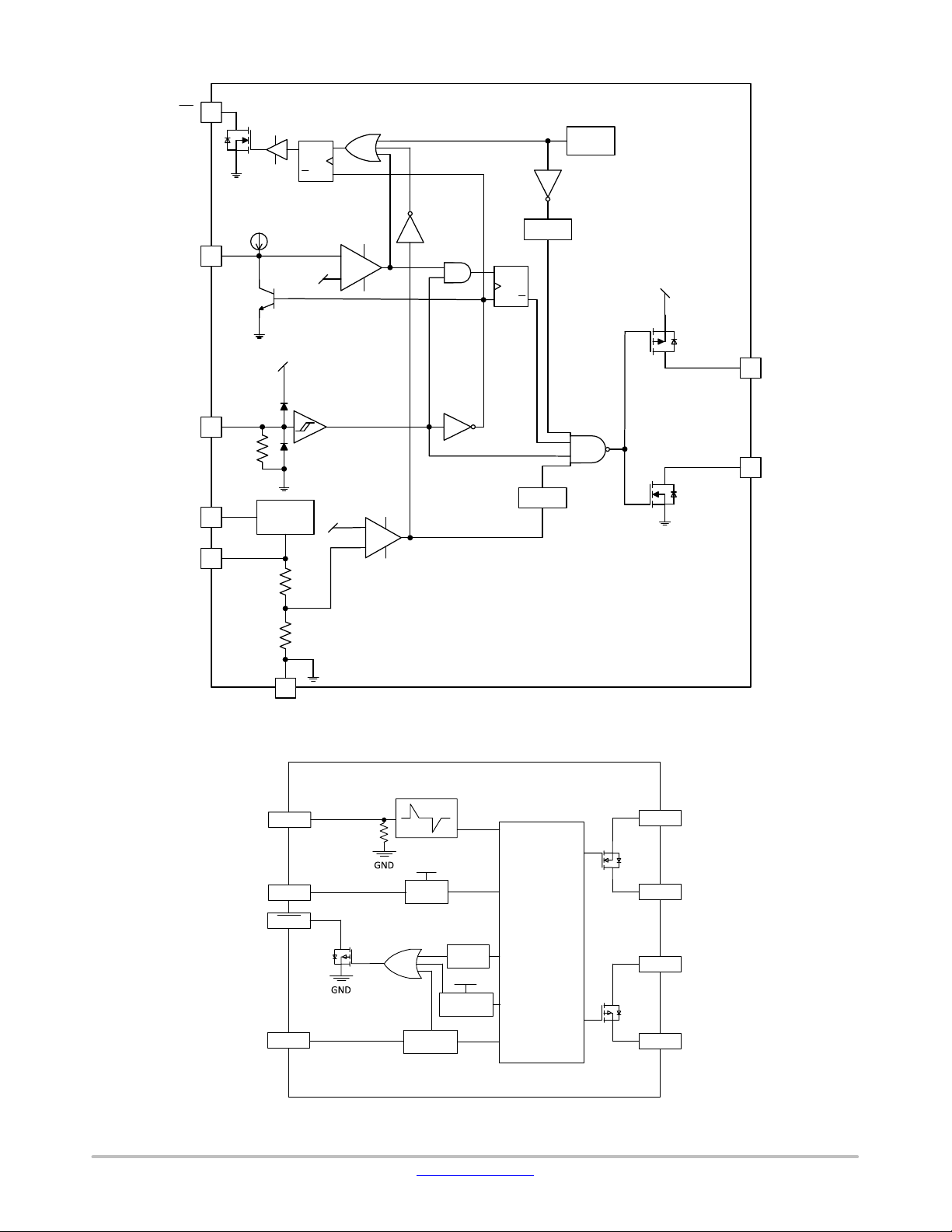
Figure 2(a). Detailed Block Diagram NCD5703A
NCD5703A
CLAMP
VIN
VCC
VREF
FLT
LDO
TSD
VCC
Logic Unit
UVLO
DESAT
Figure 2(b). Simplified Block Diagram NCD5703A
DESAT
CLAMP
GND
VO
VCC
www.onsemi.com
3
Page 4
FLT
NCD5703A, NCD5703B, NCD5703C
DESAT
V
V
V
CC
REF
SET
Q S
CLR
Q R
I
DESAT-CHG
V
DESAT-THR
V
IN
R
IN-L
+
-
REF
Bandgap
V
UVLO
-
+
SET
S Q
CLR
R Q
DELAY
DELAY
TSD
NCD5703B
V
CC
V
EE
V
O
GND
Figure 3(a). Detailed Block Diagram NCD5703B
NCD5703B
VIN
VCC
VREF
FLT
LDO
TSD
VCC
Logic Unit
UVLO
DESAT
Figure 3(b). Simplified Block Diagram NCD5703B
DESAT
VEE
GND
VO
VCC
V
EE
www.onsemi.com
4
Page 5
FLT
NCD5703A, NCD5703B, NCD5703C
DESAT
V
V
REF
V
SET
Q S
CLR
Q R
I
DESAT-CHG
V
DESAT-THR
V
REF
IN
R
IN-L
+
-
SET
S Q
CLR
R Q
DELAY
TSD
NCD5703C
V
CC
V
OH
V
OL
DELAY
Bandgap
CC
V
UVLO
-
+
GND
Figure 4(a). Detailed Block Diagram NCD5703C
NCD5703C
VIN
VCC
VREF
FLT
LDO
TSD
VCC
UVLO
DESAT
Figure 4(b). Simplified Block Diagram NCD5703C
DESAT
Logic Unit
GND
VOL
VOH
VCC
www.onsemi.com
5
Page 6
NCD5703A, NCD5703B, NCD5703C
Table 1. PIN FUNCTION DESCRIPTION
Pin Name No. I/O/x Description
VIN 1 I Input signal to control the output. In applications which require galvanic isolation, VIN is generat-
VREF 2 O 5 V Reference generated within the driver is brought out to this pin for external bypassing and
FLT 3 O Fault open drain output (active low) that allows communication to the main controller that the
DESAT 4 I Input for detecting the desaturation of IGBT due to a fault condition. A capacitor connected to
VCC 5 x Positive bias supply for the driver. The operating range for this pin is from UVLO to the maxi-
VO
(NCD5703A,
NCD5703B)
VOH
(NCD5703C)
VOL
(NCD5703C)
GND
(NCD5703A,
NCD5703B)
GND
(NCD5703C)
VEE
(NCD5703B)
CLAMP
(NCD5703A)
6 O Driver output that provides the appropriate drive voltage, source and sink current to the IGBT
6 O Driver high output that provides the appropriate drive voltage and source current to the IGBT
7 O Driver low output that provides the appropriate drive voltage and sink current to the IGBT gate.
7 x This pin should connect to the IGBT Emitter with a short trace. All power pin bypass capacitors
8 x This pin should connect to the IGBT Emitter with a short trace. All power pin bypass capacitors
8 x A negative voltage with respect to GND can be applied to this pin and that will allow VO to go to
8 I/O Provides clamping for the IGBT gate during the off period to protect it from parasitic turn−on. To
ed at the opto output, the pulse transformer secondary or the digital isolator output. VO (VOH/
VOL) signal is in phase with VIN. VIN is internally clamped to GND and has a pull−down resistor
of 1 MW to ensure that an output is low in the absence of an input signal. A minimum pulse−
width is required at VIN before VO (VOH/VOL) is activated.
for powering low bias circuits (such as digital isolators).
driver has encountered a fault condition and has deactivated the output. Open drain allows easy
setting of (inactive) high level and parallel connection of multiple fault signals.
Connect to 10k pull−up resistor recommended. Truth Table is provided in the datasheet to indicate conditions under which this signal is asserted. Capable of driving optos or digital isolators
when isolation is required.
this pin allows a programmable blanking delay every ON cycle before DESAT fault is processed,
thus preventing false triggering.
mum. A good quality bypassing capacitor is required from this pin to GND and should be placed
close to the pins for best results.
gate. VO is actively pulled low during start−up and under Fault conditions.
gate.
VOL is actively pulled low during start−up and under Fault conditions.
should be referenced to this pin and kept at a short distance from the pin.
should be referenced to this pin and kept at a short distance from the pin.
a negative voltage during OFF state. A good quality bypassing capacitor is needed from VEE to
GND. If a negative voltage is not applied or available, this pin must be connected to GND.
be tied directly to IGBT gate with minimum trace length for best results.
www.onsemi.com
6
Page 7
NCD5703A, NCD5703B, NCD5703C
Table 2. ABSOLUTE MAXIMUM RATINGS (Note 1)
Parameter Symbol Minimum Maximum Unit
Differential Power Supply VCC−VEE (V
Positive Power Supply VCC−GND −0.3 22 V
Negative Power Supply VEE−GND −18 0.3 V
Gate Output High (VO, VOH)−GND VCC + 0.3 V
Gate Output Low (VO, VOL)−GND VEE − 0.3 V
Input Voltage VIN−GND −0.3 5.5 V
DESAT Voltage V
DESAT
FLT current
Sink
Power Dissipation
I
FLT−SINK
PD 700 mW
SO−8 package
Maximum Junction Temperature T
J(max)
Storage Temperature Range TSTG −65 to 150 °C
ESD Capability, Human Body Model (Note 2) ESDHBM 4 kV
ESD Capability, Machine Model (Note 2) ESDMM 200 V
Moisture Sensitivity Level MSL 1 −
Lead Temperature Soldering
Reflow (SMD Styles Only), Pb−Free Versions (Note 3)
T
SLD
Stresses exceeding those listed in the Maximum Ratings table may damage the device. If any of these limits are exceeded, device functionality
should not be assumed, damage may occur and reliability may be affected.
1. Refer to ELECTRICAL CHARACTERISTICS and APPLICATION INFORMATION for Safe Operating Area.
2. This device series incorporates ESD protection and is tested by the following methods:
ESD Human Body Model tested per AEC−Q100−002 (EIA/JESD22−A114)
ESD Machine Model tested per AEC−Q100−003 (EIA/JESD22−A115)
Latchup Current Maximum Rating: ≤100 mA per JEDEC standard: JESD78, 25°C
3. For information, please refer to our Soldering and Mounting Techniques Reference Manual, SOLDERRM/D.
) 0 36 V
max
−GND −0.3 VCC + 0.3 V
mA
20
150 °C
260 °C
Table 3. THERMAL CHARACTERISTICS
Parameter Symbol Value Unit
Thermal Characteristics, SOIC−8 (Note 4)
Thermal Resistance, Junction−to−Air (Note 5)
4. Refer to ELECTRICAL CHARACTERISTICS and APPLICATION INFORMATION for Safe Operating Area.
5. Values based on copper area of 100 mm
2
(or 0.16 in2) of 1 oz copper thickness and FR4 PCB substrate.
R
q
JA
176
°C/W
Table 4. OPERATING RANGES (Note 6)
Parameter
Differential Power Supply VCC−VEE (V
Positive Power Supply V
Negative Power Supply V
Input Voltage V
Input pulse width t
Ambient Temperature T
6. Refer to ELECTRICAL CHARACTERISTICS and APPLICATION INFORMATION for Safe Operating Area.
Functional operation above the stresses listed in the Recommended Operating Ranges is not implied. Extended exposure to stresses beyond
the Recommended Operating Ranges limits may affect device reliability.
Symbol Min Max Unit
) 30 V
max
CC
EE
IN
on
A
UVLO 20 V
−15 0 V
0 5 V
40 ns
−40 125 °C
www.onsemi.com
7
Page 8
NCD5703A, NCD5703B, NCD5703C
Table 5. ELECTRICAL CHARACTERISTICS V
for min/max values, T
Parameter
LOGIC INPUT and OUTPUT
Input Threshold Voltages
High−state (Logic 1) Required
Low−state (Logic 0) Required
No state change
Input Current
High−state
Low−state
Input Pulse−Width
No Response at the Output
Guaranteed Response at the
Output
FLT Threshold Voltage
Low State
High State
DRIVE OUTPUT
Output Low State
Output High State
Peak Driver Current, Sink
(Note 7)
Peak Driver Current, Source
(Note 7)
DYNAMIC CHARACTERISTICS
Turn−on Delay
(see timing diagram)
Turn−off Delay
(see timing diagram)
Propagation Delay Distortion
− t
(=t
pd−on
pd−off
Prop Delay Distortion between
Parts (Note 7)
Rise Time (Note 7)
(see timing diagram)
Fall Time (Note 7)
(see timing diagram)
Delay from FLT under UVLO/
TSD to VO/VOL
Delay from DESAT to VO/VOL
(Note 7)
7. Values based on design and/or characterization.
is the operating ambient temperature range that applies, unless otherwise noted.
A
Test Conditions Symbol Min Ty p Max Unit
Pulse−Width = 150 ns, V
Voltage applied to get output to go high
Voltage applied to get output to go low
Voltage applied without change in output state
V
= 4.5 V
IN−H
V
= 0.5 V
IN−L
Voltage thresholds consistent with input
specs
(I
FLT−SINK
= 15 mA)
External pull−up
I
= 200 mA, TA = 25°C
sink
I
= 200 mA, TA = −40°C to 125°C
sink
I
= 1.0 A, TA = 25°C
sink
I
= 200 mA, TA = 25°C
src
I
= 200 mA, TA = −40°C to 125°C
src
I
= 1.0 A, TA = 25°C
src
RG = 0.1 W, VCC = 15 V, VEE = −8 V
V
= 13 V
O
V
= 9 V (near Miller Plateau)
O
RG = 0.1 W, VCC = 15 V, VEE = −8 V
V
= −5 V
O
V
= 9 V (near Miller Plateau)
O
Negative input pulse width = 10 ms
Positive input pulse width = 10 ms
For input or output pulse width > 150 ns,
)
= 25°C
T
A
T
= −40°C to 125°C
A
C
= 1.0 nF t
load
C
= 1.0 nF t
load
= 15 V, VEE = 0 V, Kelvin GND connected to VEE. For typical values TA = 25°C,
CC
= 5 V
EN
V
IN−H1
V
IN−L1
V
IN−NC
I
IN−H
I
IN−L
t
on−min1
t
on−min2
V
FLT−L
V
FLT−H
V
OL1
V
OL2
V
OL3
V
OH1
V
OH2
V
OH3
I
PK−snk1
I
PK−snk2
I
PK−src1
I
PK−src2
t
pd−on
t
pd−off
t
distort1
t
distort2
t
distort −tot
rise
fall
t
d1−OUT
t
d2−OUT
4.3
0.75
1.2
3.7
10
1
15
35
0.5 1.0
V
+0.3
CC
14.5
14.2
13.8
0.1
0.2
0.8
14.8
14.7
14.1
0.2
0.5
1.2
6.8
6.1
7.8
4.0
45 59 75 ns
45 54 75 ns
−5
−25
5 15
25
−30 0 30 ns
9.2 ns
7.9 ns
10 12 15
220 ns
V
mA
ns
V
V
V
A
A
ns
ms
www.onsemi.com
8
Page 9

NCD5703A, NCD5703B, NCD5703C
Table 5. ELECTRICAL CHARACTERISTICS V
for min/max values, T
is the operating ambient temperature range that applies, unless otherwise noted.
A
= 15 V, VEE = 0 V, Kelvin GND connected to VEE. For typical values TA = 25°C,
CC
Parameter UnitMaxTypMinSymbolTest Conditions
DYNAMIC CHARACTERISTICS
Delay from UVLO/TSD to FLT
(Note 7)
t
d3−FLT
7.3
ms
MILLER CLAMP (NCD5703A ONLY)
I
Clamp Voltage
= 500 mA, TA = 25°C
sink
I
= 500 mA, TA = −40°C to 125°C
sink
Clamp Activation Threshold V
V
clamp
MC−THR
1.2 1.4
2.2
1.8 2.0 2.2 V
V
DESAT PROTECTION
DESAT Threshold Voltage
Blanking Charge Current I
Blanking Discharge Current I
V
DESAT−THR
DESAT−CHG
DESAT−DIS
6.0 6.35 7.0 V
0.20 0.24 0.28 mA
30 mA
UVLO
UVLO Startup Voltage
V
UVLO Disable Voltage V
UVLO Hysteresis V
UVLO−OUT−ON
UVLO−OUT−OFF
UVLO−HYST
13.2 13.5 13.8 V
12.2 12.5 12.8 V
1.0 V
VREF
I
Voltage Reference
= 10 mA V
REF
Reference Output Current
(Note 7)
Recommended Capacitance C
REF
I
REF
VREF
4.85 5.00 5.15 V
20 mA
100 nF
SUPPLY CURRENT
Current Drawn from V
Current Drawn from V
(NCD5703B ONLY)
CC
EE
VCC = 15 V
Standby (No load on output, FLT
VEE = −10 V
Standby (No load on output, FLT
, VREF)
, VREF)
I
CC−SB
I
EE−SB
0.9 1.5 mA
−0.2 −0.14 mA
THERMAL SHUTDOWN
Thermal Shutdown Temperature
(Note 7)
Thermal Shutdown Hysteresis
(Note 7)
T
SD
T
SH
188 °C
33 °C
7. Values based on design and/or characterization.
Product parametric performance is indicated in the Electrical Characteristics for the listed test conditions, unless otherwise noted. Product
performance may not be indicated by the Electrical Characteristics if operated under different conditions.
ORDERING INFORMATION
Device Package Shipping
NCD5703ADR2G SOIC−8
2500 / Tape & Reel
(Pb−Free)
NCD5703BDR2G SOIC−8
2500 / Tape & Reel
(Pb−Free)
NCD5703CDR2G SOIC−8
2500 / Tape & Reel
(Pb−Free)
†For information on tape and reel specifications, including part orientation and tape sizes, please refer to our Tape and Reel Packaging
Specifications Brochure, BRD8011/D.
†
www.onsemi.com
9
Page 10
NCD5703A, NCD5703B, NCD5703C
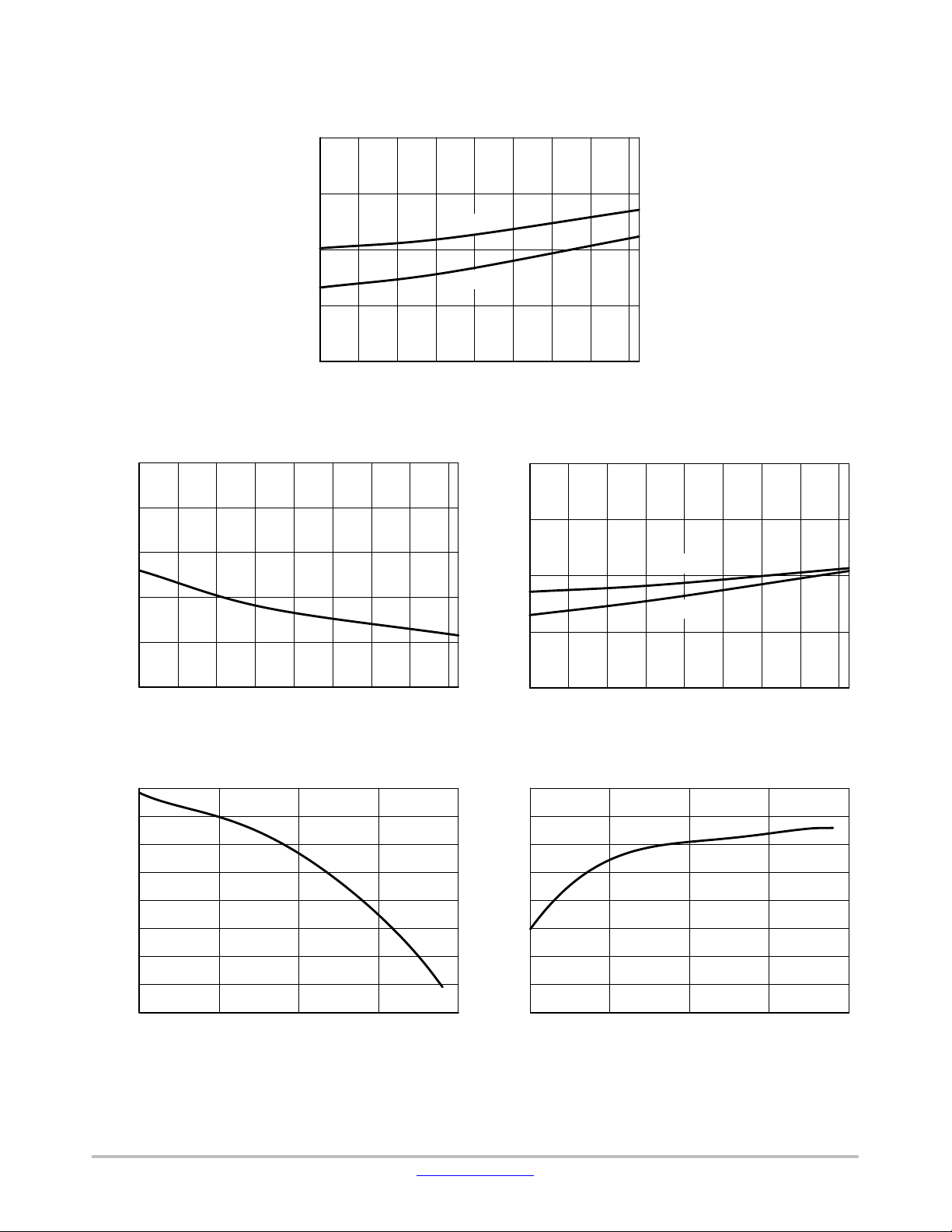
TYPICAL CHARACTERISTICS
80
70
t
pd−on
60
t
pd−off
50
PROPAGATION DELAY (ns)
40
TEMPERATURE (°C)
120
100806040200−20−40
Figure 5. Propagation Delay vs. Temperature
15
14
13
12
11
FAULT TO OUTPUT DELAY (ms)
10
TEMPERATURE (°C)
120
100806040200−20−40
20
15
10
5
RISE/FALL TIME (ns)
0
t
fall
t
rise
TEMPERATURE (°C)
120
100806040200−20−40
Figure 6. Fault to Output Low Delay Figure 7. Output Rise/Fall Time
8
7
8
7
(A)
O
I
6
5
4
3
2
1
0
VO (V, VCC = 15 V, VEE = −8 V) VO (V, VCC = 15 V, VEE = −8 V)
Figure 8. Output Source Current vs. Output
Voltage
6
5
(A)
4
O
I
3
2
1
151050−5
0
www.onsemi.com
10
151050−5
Figure 9. Output Sink Current vs. Output
Voltage
Page 11
NCD5703A, NCD5703B, NCD5703C
TYPICAL CHARACTERISTICS
(V)
REF
V
(mA)
DESET−CHG
I
5.05
5.04
5.03
5.02
5.01
5.00
4.99
4.98
4.97
4.96
4.95
260
250
Figure 10. V
5.05
5.04
5.03
5.02
V
@ I
V
REF
REF
@ I
5.01
(V)
5.00
REF
V
4.99
4.98
4.97
4.96
4.95
1086420
I
(mA) TEMPERATURE (°C)
REF
Voltage vs. Current Figure 11. V
REF
Voltage vs. Temperature
REF
6.5
6.4
(V)
DESAT
V
6.3
REF
REF
= 0 mA
= 10 mA
100806040200−20−40
120
240
15
10
5
, OUTPUT VOLTAGE (V)
O
V
0
100806040200−20−40
120
TEMPERATURE (°C) TEMPERATURE (°C)
6.2
Figure 12. DESAT Charge Current vs.
Temperature
Figure 13. DESAT Threshold Voltage vs.
Temperature
20
15
10
(V)
O
V
UVLO−OUT−OFF UVLO−OUT−ON
5
0
−5
151413121110
VCC, SUPPLY VOLTAGE (V) VIN (V)
Figure 14. UVLO Threshold Voltages Figure 15. VO vs. VIN at 255C
(V
= 15 V, VEE = 0 V)
CC
100806040200−20−40
120
543210
www.onsemi.com
11
Page 12

NCD5703A, NCD5703B, NCD5703C
TYPICAL CHARACTERISTICS
(V)
FLT−L
V
1.0
0.5
0
TEMPERATURE (°C)
Figure 16. Fault Output, Sinking 15 mA
1.4
1.2
1.0
0.8
2.5
2.0
(V)
1.5
CLAMP
V
1.0
120
100806040200−20−40
0.5
TEMPERATURE (°C)
Figure 17. V
I
CC
at 0.5 A (NCD5703A Only)
CLAMP
120
100806040200−20−40
0.6
0.4
SUPPLY CURRENT (mA)
0.2
0
Figure 18. Supply Current vs. Switching
Frequency (V
IEE (NCD5703B Only)
FREQUENCY (kHz)
= 15 V, VEE = −10 V, 255C)
CC
100806040200
www.onsemi.com
12
Page 13

NCD5703A, NCD5703B, NCD5703C
Applications and Operating Information
This section lists the details about key features and
operating guidelines for the NCD5703.
High Drive Current Capability
The NCD5703 driver family is equipped with many
features which facilitate a superior performance IGBT
driving circuit. Foremost amongst these features is the high
drive current capability. The drive current of an IGBT driver
is a function of the differential voltage on the output pin
(V
−VOH/VO for source current, VOL/VO−VEE for sink
CC
current) as shown in Figure 19. Figure 19 also indicates that
for a given VOH/VOL value, the drive current can be
increased by using higher V
CC/VEE
drive current tends to drop off as the output voltage goes up
(for turn−on event) or goes down (for turn−off event). As
explained in many IGBT application notes, the most critical
phase of IGBT switching event is the Miller plateau region
where the gate voltage remains constant at a voltage
(typically in 9−11 V range depending on IGBT design and
the collector current), but the gate drive current is used to
charge/discharge the Miller capacitance (C
providing a high drive current in this region, a gate driver can
significantly reduce the duration of the phase and help
reducing the switching losses. The NCD5703 addresses this
requirement by providing and specifying a high drive
current in the Miller plateau region. Most other gate driver
ICs merely specify peak current at the start of switching –
which may be a high number, but not very relevant to the
application requirement. It must be remembered that other
considerations such as EMI, diode reverse recovery
performance, etc., may lead to a system level decision to
trade off the faster switching speed against low EMI and
reverse recovery. However, the use of NCD5703 does not
preclude this trade−off as the user can always tune the drive
current by employing external series gate resistor. Important
thing to remember is that by providing a high internal drive
current capability, the NCD5703 facilitates a wide range of
gate resistors. Another value of the high current at the Miller
plateau is that the initial switching transition phase is shorter
and more controlled. Finally, the high gate driver current
(which is facilitated by low impedance internal FETs),
ensures that even at high switching frequencies, the power
dissipation from the drive circuit is primarily in the external
series resistor and more easily manageable. Experimental
results have shown that the high current drive results in
reduced turn−on energy (E
) for the IGBT switching.
ON
power supply). The
). By
GC
Figure 19. Output Current vs. Output Voltage Drop
When driving larger IGBTs for higher current
applications, the drive current requirement is higher, hence
lower R
is used. Larger IGBTs typically have high input
G
capacitance. On the other hand, if the NCD5703 is used to
drive smaller IGBT (lower input capacitance), the drive
current requirement is lower and a higher R
is used. Thus,
G
for most typical applications, the driver load RC time
constant remains fairly constant. Caution must be exercised
when using the NCD5703 with a very low load RC time
constant. Such a load may trigger internal protection
circuitry within the driver and disable the device. Figure 20
shows the recommended minimum gate resistance as a
function of IGBT gate capacitance and gate drive trace
inductance.
Figure 20. Recommended Minimum Gate Resistance
as a Function of IGBT Gate Capacitance
www.onsemi.com
13
Page 14

NCD5703A, NCD5703B, NCD5703C
Gate Voltage Range
The negative drive voltage for gate (with respect to GND,
or Emitter of the IGBT) is a robust way to ensure that the gate
voltage does not rise above the threshold voltage due to the
Miller effect. In systems where the negative power supply is
available, the VEE option offered by NCD5703B allows not
only a robust operation, but also a higher drive current for
turn−off transition. Adequate bypassing between VEE pin
and GND pin is essential if this option is used.
The V
range for the NCD5703 is quite wide and allows
CC
the user the flexibility to optimize the performance or use
available power supplies for convenience.
Under Voltage Lock Out (UVLO)
This feature ensures reliable switching of the IGBT
connected to the driver output. At the start of the driver’s
operation when V
remains turned−off. This is regardless of the signals on V
is applied to the driver, the output
CC
IN
until the VCC reaches the UVLO Output Enabled
(V
UVLO−OUT−ON
V
UVLO−OUT−ON
state of the output is controlled by signal at V
If the V
(V
UVLO−OUT−OFF
) level. After the VCC rises above the
level, the driver is in normal operation. The
.
IN
falls below the UVLO Output Disabled
CC
) level during the normal operation of the
driver, the Fault output is activated and the output is shut−down
(after a delay) and remains in this state. The driver output
does not start to react to the input signal on V
rises above the V
UVLO−OUT−ON
again. The waveform
until the V
IN
CC
showing the UVLO behavior of the driver is in Figure 21.
In an IGBT drive circuit, the drive voltage level is
important for drive circuit optimization. If V
UVLO−OUT−OFF
is too low, it will lead to IGBT being driven with insufficient
gate voltage. A quick review of IGBT characteristics can
reveal that driving IGBT with low voltage (in 10−12 V
range) can lead to a significant increase in conduction loss.
So, it is prudent to guarantee V
UVLO−OUT−OFF
at a
reasonable level (above 12 V), so that the IGBT is not forced
to operate at a non−optimum gate voltage. On the other hand,
having a very high drive voltage ends up increasing
switching losses without much corresponding reduction in
conduction loss. So, the V
UVLO−OUT−ON
value should not
be too high (generally, well below 15 V). These conditions
lead to a tight band for UVLO enable and disable voltages,
while guaranteeing a minimum hysteresis between the two
values to prevent hiccup mode operation. The NCD5703
meets these tight requirements and ensures smooth IGBT
operation. It ensures that a 15 V supply with ±8% tolerance
will work without degrading IGBT performance, and
guarantees that a fault will be reported and the IGBT will be
turned off when the supply voltage drops below 12.2 V.
A UVLO event (V
also triggers activation of FLT
voltage going below V
CC
output after a delay of t
UVLO−OUT−OFF
d3−FLT
This indicates to the controller that the driver has
encountered an issue and corrective action needs to be taken.
However, a nominal delay t
between the initiation of the FLT
= 12 ms is introduced
d1−OUT
output and actual turning
off of the output. This delay provides adequate time for the
controller to initiate a more orderly/sequenced shutdown. In
case the controller fails to do so, the driver output shutdown
ensures IGBT protection after t
Figure 21. UVLO Function and Limits
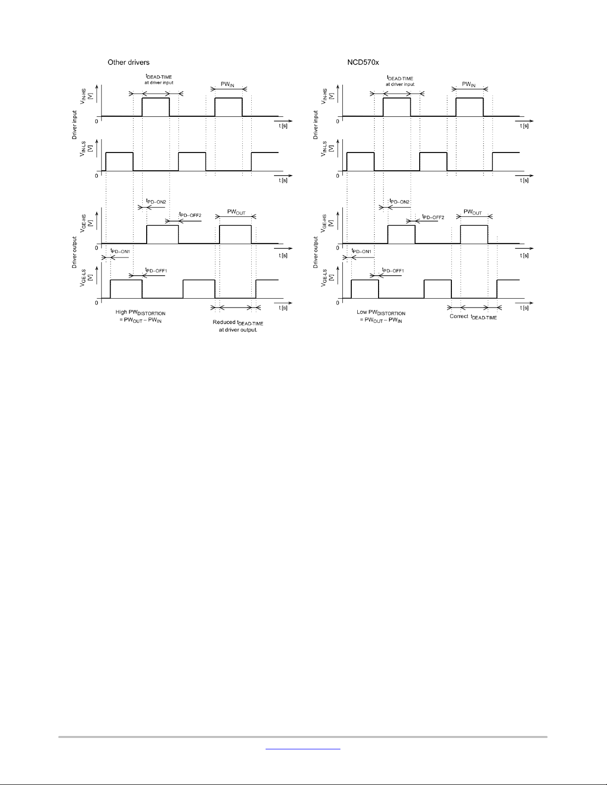
Timing Delays and Impact on System Performance
d1−OUT
.
The gate driver is ideally required to transmit the input
signal pulse to its output without any delay or distortion. In
the context of a high−power system where IGBTs are
typically used, relatively low switching frequency (in tens of
kHz) means that the delay through the driver itself may not
be as significant, but the matching of the delay between
different drivers in the same system as well as between
different edges has significant importance. With reference to
Figure 22(a), two input waveforms are shown. They are
typical complementary inputs for high−side (HS) and
low−side (LS) of a half−bridge switching configuration. The
dead−time between the two inputs ensures safe transition
between the two switches. However, once these inputs are
through the driver, there is potential for the actual gate
voltages for HS and LS to be quite different from the
intended input waveforms as shown in Figure 22(a). The end
result could be a loss of the intended dead−time and/or
pulse−width distortion. The pulse−width distortion can
create an imbalance that needs to be corrected, while the loss
of dead−time can eventually lead to cross−conduction of the
switches and additional power losses or damage to the
)
system.
.
The NCD5703 driver is designed to address these timing
challenges by providing a very low pulse−width distortion
and excellent delay matching. As an example, the delay
matching is guaranteed to t
DISTORT2
= ±25 ns while many
of competing driver solutions can be >250 ns.
www.onsemi.com
14
Page 15
NCD5703A, NCD5703B, NCD5703C
Figure 22(a). Timing Waveforms (Other Drivers) Figure 22(b). NCD5703 Timing Waveforms
Active Miller Clamp Protection
This feature (offered by NCD5703A) is a cost savvy
alternative to a negative gate voltage. The main requirement
is to hold the gate of the turned−off (for example low−side)
IGBT below the threshold voltage during the turn−on of the
opposite−side (in this example high−side) IGBT in the half
bridge. The turn−on of the high−side IGBT causes high dv/dt
transition on the collector of the turned−off low−side IGBT.
This high dv/dt then induces current (Miller current) through
the C
capacitance (Miller capacitance) to the gate
GC
capacitance of the low−side IGBT as shown in Figure 23. If
the path from gate to GND has critical impedance (caused
by R
) the Miller current could rise the gate voltage above
G
the threshold level. As a consequence the low−side IGBT
could be turned on for a few tens or hundreds of
An alternative way is to provide an additional path from
gate to GND with very low impedance. This is exactly what
Active Miller Clamp protection does. Additional trace from
the gate of the IGBT to the Clamp pin of the gate driver is
introduced. After the V
Miler Clamp threshold V
output has gone below the Active
O
MC−THR
the Clamp pin is shorted
to GND and thus prevents the voltage on the gate of the
IGBT to rise above the threshold voltage as shown in
Figure 24. The Clamp pin is disconnected from GND as
soon as the signal to turn on the IGBT arrives to the gate
driver input. The fact that the Clamp pin is engaged only
after the gate voltage drops below the V
ensures that the function of this pin does not interfere with
the normal turn−off switching performance that is user
controllable by choice of R
.
G
nanoseconds. This causes higher switching losses. One way
to avoid this situation is to use negative gate voltage, but this
requires second DC source for the negative gate voltage.
MC−THR
threshold
www.onsemi.com
15
Page 16

NCD5703A, NCD5703B, NCD5703C
Figure 23. Current Path without Miller Clamp
Protection
Desaturation Protection (DESAT)
This feature monitors the collector−emitter voltage of the
IGBT in the turned−on state. When the IGBT is fully turned
on, it operates in a saturation region. Its collector−emitter
voltage (called saturation voltage) is usually low, well below
3 V for most modern IGBTs. It could indicate an overcurrent
or similar stress event on the IGBT if the collector−emitter
voltage rises above the saturation voltage, after the IGBT is
fully turned on. Therefore the DESAT protection circuit
compares the collector−emitter voltage with a voltage level
V
DESAT−THR
to check if the IGBT didn’t leave the saturation
region. It will activate FLT output and shut down driver
output (thus turn−off the IGBT), if the saturation voltage
rises above the V
DESAT−THR
. This protection works on
every turn−on phase of the IGBT switching period.
At the beginning of turning−on of the IGBT, the
collector−emitter voltage is much higher than the saturation
voltage level which is present after the IGBT is fully turned
on. It takes almost 1 ms between the start of the IGBT turn−on
and the moment when the collector−emitter voltage falls to
the saturation level. Therefore the comparison is delayed by
a configurable time period (blanking time) to prevent false
triggering of DESAT protection before the IGBT
collector−emitter voltage falls below the saturation level.
Blanking time is set by the value of the capacitor C
BLANK
The exact principle of operation of DESAT protection is
described with reference to Figure 25.
At the turned−off output state of the driver, the DESAT pin
is shorted to ground via the discharging transistor (Q
DIS
Therefore, the inverting input holds the comparator output
at low level.
Figure 24. Current Path with Miller Clamp Protection
At the turned−on output state of the driver, the current
I
DESAT−CHG
blanking capacitor C
from current source starts to flow to the
, connected to DESAT pin.
BLANK
Appropriate value of this capacitor has to be selected to
ensure that the DESAT pin voltage does not rise above the
threshold level V
DESAT−THR
before the IGBT fully turns on.
The blanking time is given by following expression.
According to this expression, a 47 pF C
BLANK
a blanking time of (47p *6.5/0.25m =) 1.22 ms.
V
t
+ C
BLANK
BLANK
After the IGBT is fully turned−on, the I
DESAT−THR
@
I
DESAT−CHG
DESAT−CHG
through the DESAT pin to the series resistor R
through the high voltage diode and then through the
collector and IGBT to the emitter. Care must be taken to
select the resistor R
S−DESAT
value so that the sum of the
saturation voltage, drop on the HV diode and drop on the
R
S−DESAT
caused by current I
DESAT−CHG
DESAT source current is smaller than the DESAT threshold
voltage. Following expression can be used:
V
DESAT−THR
R
S−DESAT
.
Important part for DESAT protection to work properly is
u
@ I
DESAT−CHG
) V
F_HV diode
) V
the high voltage diode. It must be rated for at least same
voltage as the low side IGBT. The safety margin is
application dependent.
).
The typical waveforms for IGBT overcurrent condition
are outlined in Figure 26.
will provide
flows
S−DESAT
and
flowing from
CESAT_IGBT
www.onsemi.com
16
Page 17

NCD5703A, NCD5703B, NCD5703C
Figure 25. Desaturation Protection Schematic
Figure 26. Desaturation Protection Waveforms
www.onsemi.com
17
Page 18

NCD5703A, NCD5703B, NCD5703C
Input Signal
The input signal controls the gate driver output. Figure 27
shows the typical connection diagrams for isolated
Figure 27. Opto−coupler or Pulse Transformer At Input
applications where the input is coming through an
opto−coupler or a pulse transformer.
The relationship between gate driver input signal from a
pulse transformer (Figure 28) or opto−coupler (Figure 29)
and the output is defined by many time and voltage values.
The time values include output turn−on and turn−off delays
(t
pd−on
and t
), output rise and fall times (t
pd−off
and minimum input pulse−width (t
V
IN-H1
V
IN-NC
V
IN
t
pd-on
V
OUT
t
rise
Figure 28. Input and Output Signal Parameters for Pulse Transformer
on−min
V
IN-L1
t
pd-on
and t
rise
fall
). Note that the
t
fall
delay times are defined from 50% of input transition to first
10% of the output transition to eliminate the load
dependency. The input voltage parameters include input
high (V
input range for which no output change is initiated
)
(V
IN−NC
) and low (V
IN−H1
).
) thresholds as well as the
IN−L1
t
on-min
90%
10%
www.onsemi.com
18
Page 19

NCD5703A, NCD5703B, NCD5703C
V
IN-H1
V
IN-NC
V
IN
t
V
pd-on
OUT
t
rise
Use of VREF Pin
The NCD5703 provides an additional 5.0 V output
(VREF) that can serve multiple functions. This output is
capable of sourcing up to 10 mA current for functions such
as opto−coupler interface or external comparator interface.
The VREF pin should be bypassed with at least a 100 nF
capacitor (higher the better) irrespective of whether it is
being utilized for external functionality or not. VREF is
V
IN-L1
t
t
pd-on
fall
Figure 29. Input and Output Signal Parameters for Opto−coupler
t
on-min
90%
10%
highly stable over temperature and line/load variations (see
characteristics curves for details)
Fault Output Pin
This pin provides the feedback to the controller about the
driver operation. The situations in which the FLT
signal
becomes active (low value) are summarized in the Table 6.
Table 6. FLT LOGIC TRUTH TABLE
VIN UVLO DESAT Internal TSD VOUT FLT Notes
L Inactive L L L Open drain Normal operation − Output Low
H Inactive L L H Open drain Normal operation − Output High
X Active X L L L
H Inactive H L L L DESAT activated (only when VIN is High) − Output
X Inactive X H L L
UVLO activated − FLT Low (t
+ t
(t
d3-FLT
Low (t
d2_OUT
Internal Thermal Shutdown − FLT Low (t
put Low (t
d1−OUT
), FLT Low
d3-FLT
)
+ t
d1−OUT
)
d3-FLT
), Output Low
Thermal Shutdown
The NCD5703 also offers thermal shutdown function that
is primarily meant to self−protect the driver in the event that
the internal temperature gets excessive. Once the
temperature crosses the T
activated after a delay of t
threshold, the FLT output is
SD
. After a delay of t
d3-FLT
d1−OUT
(12 ms), the output is pulled low and many of the internal
circuits are turned off. The 12 ms delay is meant to allow the
controller to perform an orderly shutdown sequence as
appropriate. Once the temperature goes below the second
threshold, the part becomes active again.
d3-FLT
), Out-
www.onsemi.com
19
Page 20

MECHANICAL CASE OUTLINE
PACKAGE DIMENSIONS
8
1
SCALE 1:1
−Y−
−Z−
−X−
A
58
B
1
4
G
H
D
0.25 (0.010) Z
M
SOLDERING FOOTPRINT*
7.0
0.275
SOIC−8 NB
CASE 751−07
ISSUE AK
DATE 16 FEB 2011
NOTES:
1. DIMENSIONING AND TOLERANCING PER
ANSI Y14.5M, 1982.
2. CONTROLLING DIMENSION: MILLIMETER.
3. DIMENSION A AND B DO NOT INCLUDE
MOLD PROTRUSION.
4. MAXIMUM MOLD PROTRUSION 0.15 (0.006)
PER SIDE.
5. DIMENSION D DOES NOT INCLUDE DAMBAR
S
0.25 (0.010)
M
M
Y
K
Y
C
SXS
SEATING
PLANE
0.10 (0.004)
N
X 45
_
M
J
PROTRUSION. ALLOWABLE DAMBAR
PROTRUSION SHALL BE 0.127 (0.005) TOTAL
IN EXCESS OF THE D DIMENSION AT
MAXIMUM MATERIAL CONDITION.
6. 751−01 THRU 751−06 ARE OBSOLETE. NEW
STANDARD IS 751−07.
MILLIMETERS
DIMAMIN MAX MIN MAX
4.80 5.00 0.189 0.197
B 3.80 4.00 0.150 0.157
C 1.35 1.75 0.053 0.069
D 0.33 0.51 0.013 0.020
G 1.27 BSC 0.050 BSC
H 0.10 0.25 0.004 0.010
J 0.19 0.25 0.007 0.010
K 0.40 1.27 0.016 0.050
M 0 8 0 8
____
N 0.25 0.50 0.010 0.020
S 5.80 6.20 0.228 0.244
INCHES
GENERIC
MARKING DIAGRAM*
8
XXXXXX
AYWW
1
Discrete
(Pb−Free)
G
1.52
0.060
4.0
0.155
8
XXXXX
ALYWX
1
8
XXXXX
ALYWX
G
1
IC
IC
(Pb−Free)
XXXXX = Specific Device Code
A = Assembly Location
L = Wafer Lot
Y = Year
W = Work Week
G = Pb−Free Package
8
XXXXXX
AYWW
1
Discrete
XXXXXX = Specific Device Code
A = Assembly Location
Y = Year
WW = Work Week
G = Pb−Free Package
0.6
0.024
1.270
0.050
SCALE 6:1
ǒ
inches
mm
Ǔ
*This information is generic. Please refer to
device data sheet for actual part marking.
Pb−Free indicator, “G” or microdot “G”, may
or may not be present. Some products may
not follow the Generic Marking.
*For additional information on our Pb−Free strategy and soldering
details, please download the ON Semiconductor Soldering and
Mounting Techniques Reference Manual, SOLDERRM/D.
STYLES ON PAGE 2
DOCUMENT NUMBER:
DESCRIPTION:
ON Semiconductor and are trademarks of Semiconductor Components Industries, LLC dba ON Semiconductor or its subsidiaries in the United States and/or other countries.
ON Semiconductor reserves the right to make changes without further notice to any products herein. ON Semiconductor makes no warranty, representation or guarantee regarding
the suitability of its products for any particular purpose, nor does ON Semiconductor assume any liability arising out of the application or use of any product or circuit, and specifically
disclaims any and all liability, including without limitation special, consequential or incidental damages. ON Semiconductor does not convey any license under its patent rights nor the
rights of others.
© Semiconductor Components Industries, LLC, 2019
98ASB42564B
SOIC−8 NB
Electronic versions are uncontrolled except when accessed directly from the Document Repository.
Printed versions are uncontrolled except when stamped “CONTROLLED COPY” in red.
PAGE 1 OF 2
www.onsemi.com
Page 21

STYLE 1:
PIN 1. EMITTER
2. COLLECTOR
3. COLLECTOR
4. EMITTER
5. EMITTER
6. BASE
7. BASE
8. EMITTER
STYLE 5:
PIN 1. DRAIN
2. DRAIN
3. DRAIN
4. DRAIN
5. GATE
6. GATE
7. SOURCE
8. SOURCE
STYLE 9:
PIN 1. EMITTER, COMMON
2. COLLECTOR, DIE #1
3. COLLECTOR, DIE #2
4. EMITTER, COMMON
5. EMITTER, COMMON
6. BASE, DIE #2
7. BASE, DIE #1
8. EMITTER, COMMON
STYLE 13:
PIN 1. N.C.
2. SOURCE
3. SOURCE
4. GATE
5. DRAIN
6. DRAIN
7. DRAIN
8. DRAIN
STYLE 17:
PIN 1. VCC
2. V2OUT
3. V1OUT
4. TXE
5. RXE
6. VEE
7. GND
8. ACC
STYLE 21:
PIN 1. CATHODE 1
2. CATHODE 2
3. CATHODE 3
4. CATHODE 4
5. CATHODE 5
6. COMMON ANODE
7. COMMON ANODE
8. CATHODE 6
STYLE 25:
PIN 1. VIN
2. N/C
3. REXT
4. GND
5. IOUT
6. IOUT
7. IOUT
8. IOUT
STYLE 29:
PIN 1. BASE, DIE #1
2. EMITTER, #1
3. BASE, #2
4. EMITTER, #2
5. COLLECTOR, #2
6. COLLECTOR, #2
7. COLLECTOR, #1
8. COLLECTOR, #1
STYLE 2:
PIN 1. COLLECTOR, DIE, #1
2. COLLECTOR, #1
3. COLLECTOR, #2
4. COLLECTOR, #2
5. BASE, #2
6. EMITTER, #2
7. BASE, #1
8. EMITTER, #1
STYLE 6:
PIN 1. SOURCE
2. DRAIN
3. DRAIN
4. SOURCE
5. SOURCE
6. GATE
7. GATE
8. SOURCE
STYLE 10:
PIN 1. GROUND
2. BIAS 1
3. OUTPUT
4. GROUND
5. GROUND
6. BIAS 2
7. INPUT
8. GROUND
STYLE 14:
PIN 1. N−SOURCE
2. N−GATE
3. P−SOURCE
4. P−GATE
5. P−DRAIN
6. P−DRAIN
7. N−DRAIN
8. N−DRAIN
STYLE 18:
PIN 1. ANODE
2. ANODE
3. SOURCE
4. GATE
5. DRAIN
6. DRAIN
7. CATHODE
8. CATHODE
STYLE 22:
PIN 1. I/O LINE 1
2. COMMON CATHODE/VCC
3. COMMON CATHODE/VCC
4. I/O LINE 3
5. COMMON ANODE/GND
6. I/O LINE 4
7. I/O LINE 5
8. COMMON ANODE/GND
STYLE 26:
PIN 1. GND
2. dv/dt
3. ENABLE
4. ILIMIT
5. SOURCE
6. SOURCE
7. SOURCE
8. VCC
STYLE 30:
PIN 1. DRAIN 1
2. DRAIN 1
3. GATE 2
4. SOURCE 2
5. SOURCE 1/DRAIN 2
6. SOURCE 1/DRAIN 2
7. SOURCE 1/DRAIN 2
8. GATE 1
SOIC−8 NB
CASE 751−07
ISSUE AK
STYLE 3:
STYLE 7:
STYLE 11:
STYLE 15:
PIN 1. DRAIN, DIE #1
2. DRAIN, #1
3. DRAIN, #2
4. DRAIN, #2
5. GATE, #2
6. SOURCE, #2
7. GATE, #1
8. SOURCE, #1
PIN 1. INPUT
2. EXTERNAL BYPASS
3. THIRD STAGE SOURCE
4. GROUND
5. DRAIN
6. GATE 3
7. SECOND STAGE Vd
8. FIRST STAGE Vd
PIN 1. SOURCE 1
2. GATE 1
3. SOURCE 2
4. GATE 2
5. DRAIN 2
6. DRAIN 2
7. DRAIN 1
8. DRAIN 1
PIN 1. ANODE 1
2. ANODE 1
3. ANODE 1
4. ANODE 1
5. CATHODE, COMMON
6. CATHODE, COMMON
7. CATHODE, COMMON
8. CATHODE, COMMON
STYLE 19:
PIN 1. SOURCE 1
2. GATE 1
3. SOURCE 2
4. GATE 2
5. DRAIN 2
6. MIRROR 2
7. DRAIN 1
8. MIRROR 1
STYLE 23:
PIN 1. LINE 1 IN
2. COMMON ANODE/GND
3. COMMON ANODE/GND
4. LINE 2 IN
5. LINE 2 OUT
6. COMMON ANODE/GND
7. COMMON ANODE/GND
8. LINE 1 OUT
STYLE 27:
PIN 1. ILIMIT
2. OVLO
3. UVLO
4. INPUT+
5. SOURCE
6. SOURCE
7. SOURCE
8. DRAIN
DATE 16 FEB 2011
STYLE 4:
PIN 1. ANODE
2. ANODE
3. ANODE
4. ANODE
5. ANODE
6. ANODE
7. ANODE
8. COMMON CATHODE
STYLE 8:
PIN 1. COLLECTOR, DIE #1
2. BASE, #1
3. BASE, #2
4. COLLECTOR, #2
5. COLLECTOR, #2
6. EMITTER, #2
7. EMITTER, #1
8. COLLECTOR, #1
STYLE 12:
PIN 1. SOURCE
2. SOURCE
3. SOURCE
4. GATE
5. DRAIN
6. DRAIN
7. DRAIN
8. DRAIN
STYLE 16:
PIN 1. EMITTER, DIE #1
2. BASE, DIE #1
3. EMITTER, DIE #2
4. BASE, DIE #2
5. COLLECTOR, DIE #2
6. COLLECTOR, DIE #2
7. COLLECTOR, DIE #1
8. COLLECTOR, DIE #1
STYLE 20:
PIN 1. SOURCE (N)
2. GATE (N)
3. SOURCE (P)
4. GATE (P)
5. DRAIN
6. DRAIN
7. DRAIN
8. DRAIN
STYLE 24:
PIN 1. BASE
2. EMITTER
3. COLLECTOR/ANODE
4. COLLECTOR/ANODE
5. CATHODE
6. CATHODE
7. COLLECTOR/ANODE
8. COLLECTOR/ANODE
STYLE 28:
PIN 1. SW_TO_GND
2. DASIC_OFF
3. DASIC_SW_DET
4. GND
5. V_MON
6. VBULK
7. VBULK
8. VIN
DOCUMENT NUMBER:
DESCRIPTION:
ON Semiconductor and are trademarks of Semiconductor Components Industries, LLC dba ON Semiconductor or its subsidiaries in the United States and/or other countries.
ON Semiconductor reserves the right to make changes without further notice to any products herein. ON Semiconductor makes no warranty, representation or guarantee regarding
the suitability of its products for any particular purpose, nor does ON Semiconductor assume any liability arising out of the application or use of any product or circuit, and specifically
disclaims any and all liability, including without limitation special, consequential or incidental damages. ON Semiconductor does not convey any license under its patent rights nor the
rights of others.
© Semiconductor Components Industries, LLC, 2019
98ASB42564B
SOIC−8 NB
Electronic versions are uncontrolled except when accessed directly from the Document Repository.
Printed versions are uncontrolled except when stamped “CONTROLLED COPY” in red.
PAGE 2 OF 2
www.onsemi.com
Page 22

ON Semiconductor and are trademarks of Semiconductor Components Industries, LLC dba ON Semiconductor or its subsidiaries in the United States and/or other countries.
ON Semiconductor owns the rights to a number of patents, trademarks, copyrights, trade secrets, and other intellectual property. A listing of ON Semiconductor’s product/patent
coverage may be accessed at www.onsemi.com/site/pdf/Patent−Marking.pdf
ON Semiconductor makes no warranty, representation or guarantee regarding the suitability of its products for any particular purpose, nor does ON Semiconductor assume any liability
arising out of the application or use of any product or circuit, and specifically disclaims any and all liability, including without limitation special, consequential or incidental damages.
Buyer is responsible for its products and applications using ON Semiconductor products, including compliance with all laws, regulations and safety requirements or standards,
regardless of any support or applications information provided by ON Semiconductor. “Typical” parameters which may be provided in ON Semiconductor data sheets and/or
specifications can and do vary in different applications and actual performance may vary over time. All operating parameters, including “Typicals” must be validated for each customer
application by customer’s technical experts. ON Semiconductor does not convey any license under its patent rights nor the rights of others. ON Semiconductor products are not
designed, intended, or authorized for use as a critical component in life support systems or any FDA Class 3 medical devices or medical devices with a same or similar classification
in a foreign jurisdiction or any devices intended for implantation in the human body. Should Buyer purchase or use ON Semiconductor products for any such unintended or unauthorized
application, Buyer shall indemnify and hold ON Semiconductor and its officers, employees, subsidiaries, affiliates, and distributors harmless against all claims, costs, damages, and
expenses, and reasonable attorney fees arising out of, directly or indirectly, any claim of personal injury or death associated with such unintended or unauthorized use, even if such
claim alleges that ON Semiconductor was negligent regarding the design or manufacture of the part. ON Semiconductor is an Equal Opportunity/Affirmative Action Employer. This
literature is subject to all applicable copyright laws and is not for resale in any manner.
. ON Semiconductor reserves the right to make changes without further notice to any products herein.
PUBLICATION ORDERING INFORMATION
LITERATURE FULFILLMENT:
Email Requests to: orderlit@onsemi.com
ON Semiconductor Website: www.onsemi.com
TECHNICAL SUPPORT
North American Technical Support:
Voice Mail: 1 800−282−9855 Toll Free USA/Canada
Phone: 011 421 33 790 2910
Europe, Middle East and Africa Technical Support:
Phone: 00421 33 790 2910
For additional information, please contact your local Sales Representative
◊
www.onsemi.com
1
 Loading...