

Page 1
TinyLogic UHS Dual Buffer
NC7WZ16
Description
The NC7WZ16 is a dual buffer from ON Semiconductor’s
Ultra−High Speed Series of TinyLogic. The device is fabricated with
advanced CMOS technology to achieve ultra−high speed with high
output drive while maintaining low static power dissipation over a
very broad V
over the 1.65 V to 5.5 V V
impedance when V
independent of V
Features
• Ultra−High Speed: t
• High Output Drive: ±24 mA at 3 V V
• Broad V
• Matches Performance of LCX when Operated at 3.3 V V
• Power Down High−Impedance Inputs / Outputs
• Over−Voltage Tolerance Inputs Facilitate 5 V to 3 V Translation
• Proprietary Noise / EMI Reduction Circuitry
• Ultra−Small MicroPak Packages
• Space−Saving SC−88 Package
• These Devices are Pb−Free, Halogen Free/BFR Free and are RoHS
Compliant
operating range. The device is specified to operate
CC
range. The inputs and outputs are high
CC
is 0 V. Inputs tolerate voltages up to 5.5 V
CC
operating voltage.
CC
= 2.4 ns (Typical) into 50 pF at 5 V V
PD
CC
Operating Range: 1.65 V to 5.5 V
CC
CC
CC
www.onsemi.com
SIP6 1.45x1.0
CASE 127EB
Pin 1
UDFN6
1.0X1.0, 0.35P
CASE 517DP
Pin 1
SC−88
CASE 419B−02
MARKING
DIAGRAMS
C7KK
XYZ
C7KK
XYZ
6
Z16MG
G
1
IEEC / IEC
A
1
A
2
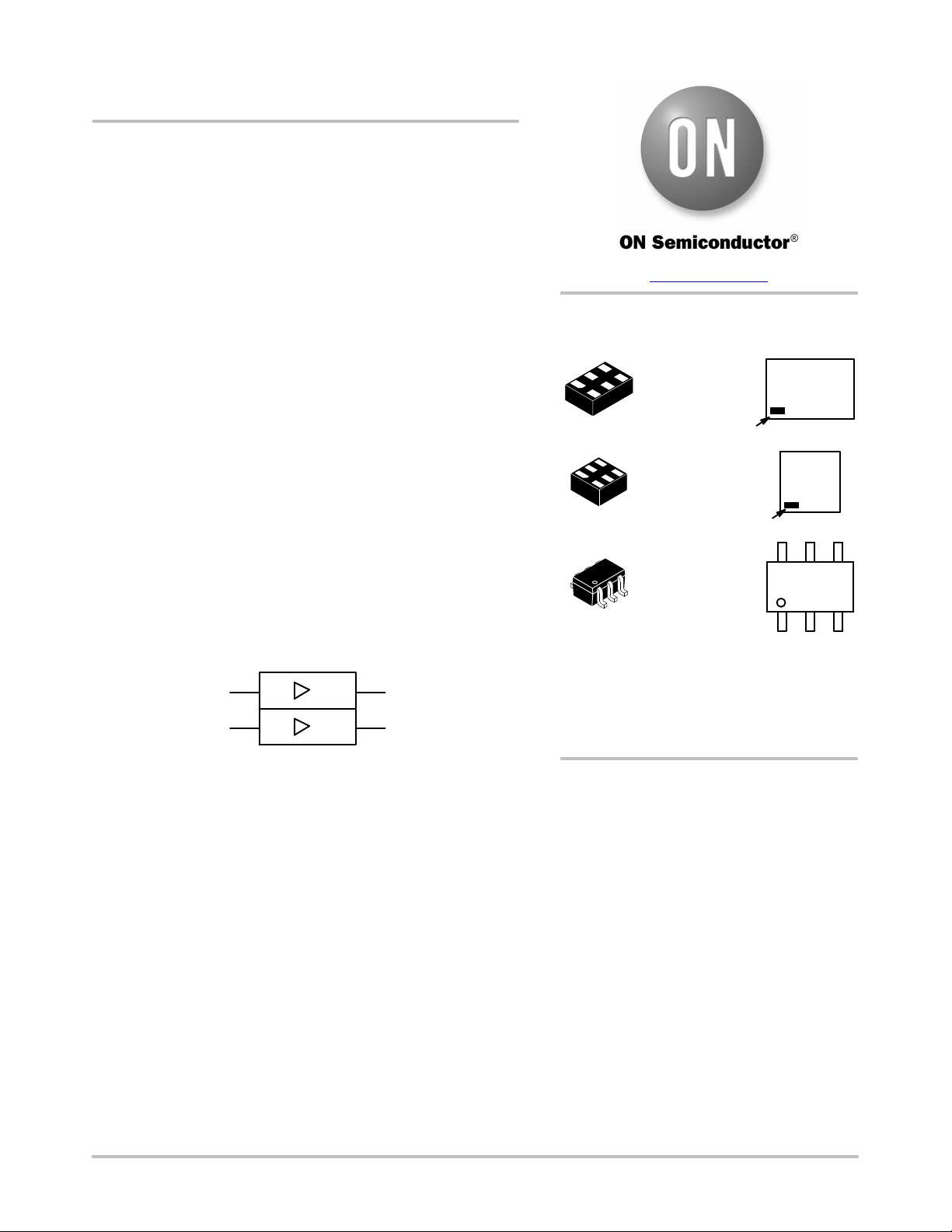
Figure 1. Logic Symbol
1
1
C7, Z16 = Specific Device Code
KK = 2−Digit Lot Run Traceability Code
Y
1
Y
2
XY = 2−Digit Date Code Format
Z = Assembly Plant Code
M = Assembly Operation Month
G = Pb−Free Package
ORDERING INFORMATION
See detailed ordering, marking and shipping information in the
package dimensions section on page 6 of this data sheet.
Semiconductor Components Industries, LLC, 1999
February, 2021 − Rev. 4
1 Publication Order Number:
NC7WZ16/D
Page 2
Pin Configurations
NC7WZ16
A
1
1
GND V
2
A
3
2
Y
6
1
5
CC
Y
4
2
Figure 2. SC−88 (Top View)
(Top View) AAA
Pin One
NOTES:
1. AAA represents product code top mark (see ordering table).
2. Orientation of Top Mark determines Pin One location. Read the
top product code mark left to right, Pin One is the lower left pin.
Figure 4. Pin 1 Orientation
PIN DEFINITIONS
Pin # SC−88 Pin # MicroPak Name Description
1 1 A
2 2 GND Ground
3 3 A
4 4 Y
5 5 V
6 6 Y
1
2
2
CC
1
Input
Input
Output
Supply Voltage
Output
A1 1 6 Y
GND 2 5 V
A2 3 4 Y
Figure 3. MicroPak (Top Through View)
FUNCTION TABLE (Y = A)
Inputs
A Y
L L
H H
H = HIGH Logic Level
L LOW Logic Level
1
CC
2
Output
www.onsemi.com
2
Page 3
NC7WZ16
ABSOLUTE MAXIMUM RATINGS
Symbol Parameter Min Max Unit
V
CC
V
IN
V
OUT
I
IK
I
OK
I
OUT
ICC or I
T
STG
T
J
T
L
P
D
ESD
Stresses exceeding those listed in the Maximum Ratings table may damage the device. If any of these limits are exceeded, device functionality
should not be assumed, damage may occur and reliability may be affected.
Supply Voltage −0.5 6.5 V
DC Input Voltage −0.5 6.5 V
DC Output Voltage −0.5 6.5 V
DC Input Diode Current VIN < 0 V − −50 mA
DC Output Diode Current V
< 0 V − −50 mA
OUT
DC Output Source / Sink Current − ±50 mA
DC VCC or Ground Current − ±50 mA
GND
Storage Temperature Range −65 +150 °C
Junction Temperature Under Bias − +150 °C
Junction Lead Temperature (Soldering, 10 Seconds) − +260 °C
Power Dissipation in Still Air
SC−88 − 332
MicroPak−6 − 812
MicroPak2−6 − 812
Human Body Model, JEDEC: JESD22−A114 − 4000
Charge Device Model, JEDEC: JESD22−C101 − 2000
mW
V
RECOMMENDED OPERATING CONDITIONS
Symbol Parameter Conditions Min Max Unit
V
CC
Supply Voltage Operating 1.65 5.50
Supply Voltage Data Retention 1.50 5.50
V
V
OUT
tr, t
IN
Input Voltage 0 5.5 V
Output Voltage 0 V
Input Rise and Fall Times
f
VCC = 1.8 V, 2.5 V ±0.2 V 0 20
CC
VCC = 3.3 V ±0.3 V 0 10
VCC = 5.5 V ±0.5 V 0 5
T
q
JA
Operating Temperature −40 +125 °C
A
Thermal Resistance
SC−88 − 377
MicroPak − 154
MicroPak2 − 154 °C/W
Functional operation above the stresses listed in the Recommended Operating Ranges is not implied. Extended exposure to stresses beyond
the Recommended Operating Ranges limits may affect device reliability.
3. Unused inputs must be held HIGH or LOW. They may not float.
V
V
ns/V
°C/W
www.onsemi.com
3
Page 4
DC ELECTICAL CHARACTERISTICS
Symbol Parameter V
V
IH
HIGH Level
Control Input
Voltage
V
IL
LOW Level
Control Input
Voltage
V
V
I
OFF
I
I
OH
OL
IN
CC
HIGH Level
Output Voltage
LOW Level
Output Voltage
Input Leakage
Current
Power Off
Leakage Current
Quiescent
Supply Current
(V) Conditions
CC
1.65 to 1.95 0.65 V
2.3 to 5.5 0.70 V
1.65 to 1.95 − − 0.35 V
2.3 to 5.5 − − 0.30 V
1.65
1.80 1.70 1.80 − 1.70 −
2.30 2.20 2.30 − 2.20 −
3.00 2.90 3.00 − 2.90 −
4.50 4.40 4.50 − 4.40 −
1.65 I
2.30 I
3.00 I
3.00 I
4.50 I
1.65
1.80 − 0.00 0.10 − 0.10
2.30 − 0.00 0.10 − 0.10
3.00 − 0.00 0.10 − 0.10
4.50 − 0.00 0.10 − 0.10
1.65 I
2.30 I
3.00 I
3.00 I
4.50 I
1.65 to 5.5 0 ≥ VIN ≥ 5.5 V − − ±0.1 − ±1.0
0 VIN or
1.65 to 5.50 V
V
IN
or V
V
IN
or V
= V
= V
NC7WZ16
TA = 25°C TA = −40 to 85°C
Min Typ Max Min Max
− − 0.65 V
CC
− − 0.70 V
CC
CC
CC
I
= −100 mA 1.55 1.65 − 1.55 −
IH
OH
IL
= −4 mA 1.29 1.52 − 1.21 −
OH
= −8 mA 1.90 2.14 − 1.90 −
OH
= −16 mA 2.40 2.75 − 2.40 −
OH
= −24 mA 2.30 2.62 − 2.30 −
OH
= −32 mA 3.80 4.13 − 3.80 −
OH
I
= 100 mA − 0.00 0.10 − 0.10
IH
OL
IL
= 4 mA − 0.08 0.24 − 0.24
OL
= 8 mA − 0.10 0.30 − 0.30
OL
= 16 mA − 0.16 0.40 − 0.40
OL
= 24 mA − 0.24 0.55 − 0.55
OL
= 32 mA − 0.25 0.55 − 0.55
OL
CC
CC
− 0.35 V
− 0.30 V
− − 1.0 − 10
V
= 5.5 V
OUT
= 5.5 V, GND − − 1.0 − 10
IN
Unit
−
V
−
V
CC
CC
V
V
mA
mA
mA
www.onsemi.com
4
Page 5

NC7WZ16
AC ELECTRICAL CHARACTERISTICS
TA = 25°C TA = −40 to 85°C
Symbol Parameter V
t
, t
PLH
C
C
Propagation Delay
PHL
(Figure 5, 6)
Input Capacitance 0 − 2.5 − − − pF
IN
Power Dissipation Capacitance
PD
(Note 4)
(Figure 7)
4. CPD is defined as the value of the internal equivalent capacitance which is derived from dynamic operating current consumption (I
no output loading and operating at 50% duty cycle. C
= (CPD) (VCC) (fIN) + (ICCstatic).
I
CCD
(V) Conditions Min Typ Max Min Max Unit
CC
C
1.65
1.80 − 4.6 8.0 − 8.8
L
R
L
= 15 pF,
= 1 MW
− 5.5 9.6 − 10.6
2.50 ±0.20 − 3.0 5.2 − 5.8
3.30 ±0.30 − 2.3 3.6 − 4.0
5.00 ±0.50 − 1.8 2.9 − 3.2
C
3.30 ±0.30
5.00 ±0.50 − 2.4 3.8 − 4.2
L
R
L
= 50 pF,
= 500 W
− 3.0 4.6 − 5.1
3.30 − 10 − − −
5.00 − 12 − − −
is related to I
PD
dynamic operating current by the expression:
CCD
CCD
ns
pF
) at
= 3 ns
t
V
CC
INPUT OUTPUT
C
R
L
L
NOTE:
includes load and stray capacitance;
5. C
L
inputs PRR = 1.0 MHz, t
= 500 ns.
W
r
INPUT
OUTPUT
10%
90%
50% 50%
t
PHL
50%
Figure 5. AC Test Circuit Figure 6. AC Waveforms
V
CC
A
INPUT
NOTE:
6. Input = AC Waveform; t
PRR = 10 MHz; Duty Cycle = 50%.
Figure 7. I
CCD
= t
= 1.8 ns;
r
f
Test Circuit
tf = 3 ns
V
90%
t
PLH
10%
t
W
CC
GND
V
OH
50%
V
OL
www.onsemi.com
5
Page 6

NC7WZ16
DEVICE ORDERING INFORMATION
Device Top Mark Packages Shipping
NC7WZ16P6X Z16 6−Lead SC70, EIAJ SC−88, 1.25 mm Wide 3000 / Tape & Reel
NC7WZ16L6X C7 6−Lead MicroPak, 1.00 mm Wide 5000 / Tape & Reel
NC7WZ16FHX C7 6−Lead, MicroPak2, 1x1 mm Body, .35 mm Pitch 5000 / Tape & Reel
†For information on tape and reel specifications, including part orientation and tape sizes, please refer to our Tape and Reel Packaging
Specifications Brochure, BRD8011/D.
†
MicroPak and MicroPak2 are trademarks of Semiconductor Components Industries, LLC (SCILLC) or its subsidiaries in the United States and/or other
countries.
www.onsemi.com
6
Page 7

MECHANICAL CASE OUTLINE
PACKAGE DIMENSIONS
SIP6 1.45X1.0
CASE 127EB
ISSUE O
DATE 31 AUG 2016
DOCUMENT NUMBER:
DESCRIPTION:
ON Semiconductor and are trademarks of Semiconductor Components Industries, LLC dba ON Semiconductor or its subsidiaries in the United States and/or other countries.
ON Semiconductor reserves the right to make changes without further notice to any products herein. ON Semiconductor makes no warranty, representation or guarantee regarding
the suitability of its products for any particular purpose, nor does ON Semiconductor assume any liability arising out of the application or use of any product or circuit, and specifically
disclaims any and all liability, including without limitation special, consequential or incidental damages. ON Semiconductor does not convey any license under its patent rights nor the
rights of others.
© Semiconductor Components Industries, LLC, 2019
98AON13590G
SIP6 1.45X1.0
Electronic versions are uncontrolled except when accessed directly from the Document Repository.
Printed versions are uncontrolled except when stamped “CONTROLLED COPY” in red.
PAGE 1 OF 1
www.onsemi.com
Page 8

MECHANICAL CASE OUTLINE
PACKAGE DIMENSIONS
SC−88/SC70−6/SOT−363
1
SCALE 2:1
D
A
654
E
123
2X
bbb H
D
e
B
TOP VIEW
6X
ccc
C
SIDE VIEW END VIEW
RECOMMENDED
SOLDERING FOOTPRINT*
6X
0.30
0.65
PITCH
*For additional information on our Pb−Free strategy and soldering
details, please download the ON Semiconductor Soldering and
Mounting Techniques Reference Manual, SOLDERRM/D.
2X
aaa H D
D
E1
L2
aaa C
2X 3 TIPS
b
6X
M
A2
A
A1
C
6X
0.66
SEATING
PLANE
2.50
DIMENSIONS: MILLIMETERS
Cddd
A-B D
DETAIL A
CASE 419B−02
ISSUE Y
H
L
DETAIL A
GAGE
PLANE
DATE 11 DEC 2012
NOTES:
1. DIMENSIONING AND TOLERANCING PER ASME Y14.5M, 1994.
2. CONTROLLING DIMENSION: MILLIMETERS.
3. DIMENSIONS D AND E1 DO NOT INCLUDE MOLD FLASH,
PROTRUSIONS, OR GATE BURRS. MOLD FLASH, PROTRUSIONS, OR GATE BURRS SHALL NOT EXCEED 0.20 PER END.
4. DIMENSIONS D AND E1 AT THE OUTERMOST EXTREMES OF
THE PLASTIC BODY AND DATUM H.
5. DATUMS A AND B ARE DETERMINED AT DATUM H.
6. DIMENSIONS b AND c APPLY TO THE FLAT SECTION OF THE
LEAD BETWEEN 0.08 AND 0.15 FROM THE TIP.
7. DIMENSION b DOES NOT INCLUDE DAMBAR PROTRUSION.
ALLOWABLE DAMBAR PROTRUSION SHALL BE 0.08 TOTAL IN
EXCESS OF DIMENSION b AT MAXIMUM MATERIAL CONDITION. THE DAMBAR CANNOT BE LOCATED ON THE LOWER
RADIUS OF THE FOOT.
MILLIMETERS
DIM MIN NOM MAX
A −−− −−− 1.10
A1 0.00 −−− 0.10
A2 0.70 0.90 1.00 0.027 0.035 0.039
b 0.15 0.20 0.25
C 0.08 0.15 0.22
D 1.80 2.00 2.20
E
2.00 2.10 2.20
E1 1.15 1.25 1.35
e 0.65 BSC
L 0.26 0.36 0.46
L2 0.15 BSC 0.006 BSC
aaa 0.15 0.006
bbb 0.30 0.012
ccc 0.10 0.004
ddd
c
0.10 0.004
INCHES
MIN NOM MAX
−−− −−− 0.043
0.000 −−− 0.004
0.006 0.008 0.010
0.003 0.006 0.009
0.070 0.078 0.086
0.078 0.082 0.086
0.045 0.049 0.053
0.026 BSC
0.010 0.014 0.018
GENERIC
MARKING DIAGRAM*
6
XXXMG
G
1
XXX = Specific Device Code
M = Date Code*
G = Pb−Free Package
(Note: Microdot may be in either location)
*Date Code orientation and/or position may
vary depending upon manufacturing location.
*This information is generic. Please refer to
device data sheet for actual part marking.
Pb−Free indicator, “G” or microdot “G”, may
or may not be present. Some products may
not follow the Generic Marking.
STYLES ON PAGE 2
DOCUMENT NUMBER:
DESCRIPTION:
ON Semiconductor and are trademarks of Semiconductor Components Industries, LLC dba ON Semiconductor or its subsidiaries in the United States and/or other countries.
ON Semiconductor reserves the right to make changes without further notice to any products herein. ON Semiconductor makes no warranty, representation or guarantee regarding
the suitability of its products for any particular purpose, nor does ON Semiconductor assume any liability arising out of the application or use of any product or circuit, and specifically
disclaims any and all liability, including without limitation special, consequential or incidental damages. ON Semiconductor does not convey any license under its patent rights nor the
rights of others.
© Semiconductor Components Industries, LLC, 2019
98ASB42985B
SC−88/SC70−6/SOT−363
Electronic versions are uncontrolled except when accessed directly from the Document Repository.
Printed versions are uncontrolled except when stamped “CONTROLLED COPY” in red.
PAGE 1 OF 2
www.onsemi.com
Page 9

SC−88/SC70−6/SOT−363
CASE 419B−02
ISSUE Y
DATE 11 DEC 2012
STYLE 1:
PIN 1. EMITTER 2
2. BASE 2
3. COLLECTOR 1
4. EMITTER 1
5. BASE 1
6. COLLECTOR 2
STYLE 7:
PIN 1. SOURCE 2
2. DRAIN 2
3. GATE 1
4. SOURCE 1
5. DRAIN 1
6. GATE 2
STYLE 13:
PIN 1. ANODE
2. N/C
3. COLLECTOR
4. EMITTER
5. BASE
6. CATHODE
STYLE 19:
PIN 1. I OUT
2. GND
3. GND
4. V CC
5. V EN
6. V REF
STYLE 25:
PIN 1. BASE 1
2. CATHODE
3. COLLECTOR 2
4. BASE 2
5. EMITTER
6. COLLECTOR 1
STYLE 2:
CANCELLED
STYLE 8:
CANCELLED
STYLE 14:
PIN 1. VREF
2. GND
3. GND
4. IOUT
5. VEN
6. VCC
STYLE 20:
PIN 1. COLLECTOR
2. COLLECTOR
3. BASE
4. EMITTER
5. COLLECTOR
6. COLLECTOR
STYLE 26:
PIN 1. SOURCE 1
2. GATE 1
3. DRAIN 2
4. SOURCE 2
5. GATE 2
6. DRAIN 1
STYLE 3:
CANCELLED
STYLE 9:
PIN 1. EMITTER 2
2. EMITTER 1
3. COLLECTOR 1
4. BASE 1
5. BASE 2
6. COLLECTOR 2
STYLE 15:
PIN 1. ANODE 1
2. ANODE 2
3. ANODE 3
4. CATHODE 3
5. CATHODE 2
6. CATHODE 1
STYLE 21:
PIN 1. ANODE 1
2. N/C
3. ANODE 2
4. CATHODE 2
5. N/C
6. CATHODE 1
STYLE 27:
PIN 1. BASE 2
2. BASE 1
3. COLLECTOR 1
4. EMITTER 1
5. EMITTER 2
6. COLLECTOR 2
STYLE 4:
PIN 1. CATHODE
2. CATHODE
3. COLLECTOR
4. EMITTER
5. BASE
6. ANODE
STYLE 10:
PIN 1. SOURCE 2
2. SOURCE 1
3. GATE 1
4. DRAIN 1
5. DRAIN 2
6. GATE 2
STYLE 16:
PIN 1. BASE 1
2. EMITTER 2
3. COLLECTOR 2
4. BASE 2
5. EMITTER 1
6. COLLECTOR 1
STYLE 22:
PIN 1. D1 (i)
2. GND
3. D2 (i)
4. D2 (c)
5. VBUS
6. D1 (c)
STYLE 28:
PIN 1. DRAIN
2. DRAIN
3. GATE
4. SOURCE
5. DRAIN
6. DRAIN
Note: Please refer to datasheet for
style callout. If style type is not called
out in the datasheet refer to the device
datasheet pinout or pin assignment.
STYLE 5:
PIN 1. ANODE
2. ANODE
3. COLLECTOR
4. EMITTER
5. BASE
6. CATHODE
STYLE 11:
PIN 1. CATHODE 2
2. CATHODE 2
3. ANODE 1
4. CATHODE 1
5. CATHODE 1
6. ANODE 2
STYLE 17:
PIN 1. BASE 1
2. EMITTER 1
3. COLLECTOR 2
4. BASE 2
5. EMITTER 2
6. COLLECTOR 1
STYLE 23:
PIN 1. Vn
2. CH1
3. Vp
4. N/C
5. CH2
6. N/C
STYLE 29:
PIN 1. ANODE
2. ANODE
3. COLLECTOR
4. EMITTER
5. BASE/ANODE
6. CATHODE
STYLE 6:
PIN 1. ANODE 2
2. N/C
3. CATHODE 1
4. ANODE 1
5. N/C
6. CATHODE 2
STYLE 12:
PIN 1. ANODE 2
2. ANODE 2
3. CATHODE 1
4. ANODE 1
5. ANODE 1
6. CATHODE 2
STYLE 18:
PIN 1. VIN1
2. VCC
3. VOUT2
4. VIN2
5. GND
6. VOUT1
STYLE 24:
PIN 1. CATHODE
2. ANODE
3. CATHODE
4. CATHODE
5. CATHODE
6. CATHODE
STYLE 30:
PIN 1. SOURCE 1
2. DRAIN 2
3. DRAIN 2
4. SOURCE 2
5. GATE 1
6. DRAIN 1
DOCUMENT NUMBER:
DESCRIPTION:
ON Semiconductor and are trademarks of Semiconductor Components Industries, LLC dba ON Semiconductor or its subsidiaries in the United States and/or other countries.
ON Semiconductor reserves the right to make changes without further notice to any products herein. ON Semiconductor makes no warranty, representation or guarantee regarding
the suitability of its products for any particular purpose, nor does ON Semiconductor assume any liability arising out of the application or use of any product or circuit, and specifically
disclaims any and all liability, including without limitation special, consequential or incidental damages. ON Semiconductor does not convey any license under its patent rights nor the
rights of others.
© Semiconductor Components Industries, LLC, 2019
98ASB42985B
SC−88/SC70−6/SOT−363
Electronic versions are uncontrolled except when accessed directly from the Document Repository.
Printed versions are uncontrolled except when stamped “CONTROLLED COPY” in red.
PAGE 2 OF 2
www.onsemi.com
Page 10

MECHANICAL CASE OUTLINE
PACKAGE DIMENSIONS
UDFN6 1.0X1.0, 0.35P
CASE 517DP
ISSUE O
DATE 31 AUG 2016
DOCUMENT NUMBER:
DESCRIPTION:
ON Semiconductor and are trademarks of Semiconductor Components Industries, LLC dba ON Semiconductor or its subsidiaries in the United States and/or other countries.
ON Semiconductor reserves the right to make changes without further notice to any products herein. ON Semiconductor makes no warranty, representation or guarantee regarding
the suitability of its products for any particular purpose, nor does ON Semiconductor assume any liability arising out of the application or use of any product or circuit, and specifically
disclaims any and all liability, including without limitation special, consequential or incidental damages. ON Semiconductor does not convey any license under its patent rights nor the
rights of others.
© Semiconductor Components Industries, LLC, 2019
98AON13593G
UDFN6 1.0X1.0, 0.35P
Electronic versions are uncontrolled except when accessed directly from the Document Repository.
Printed versions are uncontrolled except when stamped “CONTROLLED COPY” in red.
PAGE 1 OF 1
www.onsemi.com
Page 11

ON Semiconductor and are trademarks of Semiconductor Components Industries, LLC dba ON Semiconductor or its subsidiaries in the United States and/or other countries.
ON Semiconductor owns the rights to a number of patents, trademarks, copyrights, trade secrets, and other intellectual property. A listing of ON Semiconductor’s product/patent
coverage may be accessed at www.onsemi.com/site/pdf/Patent−Marking.pdf
ON Semiconductor makes no warranty, representation or guarantee regarding the suitability of its products for any particular purpose, nor does ON Semiconductor assume any liability
arising out of the application or use of any product or circuit, and specifically disclaims any and all liability, including without limitation special, consequential or incidental damages.
Buyer is responsible for its products and applications using ON Semiconductor products, including compliance with all laws, regulations and safety requirements or standards,
regardless of any support or applications information provided by ON Semiconductor. “Typical” parameters which may be provided in ON Semiconductor data sheets and/or
specifications can and do vary in different applications and actual performance may vary over time. All operating parameters, including “Typicals” must be validated for each customer
application by customer’s technical experts. ON Semiconductor does not convey any license under its patent rights nor the rights of others. ON Semiconductor products are not
designed, intended, or authorized for use as a critical component in life support systems or any FDA Class 3 medical devices or medical devices with a same or similar classification
in a foreign jurisdiction or any devices intended for implantation in the human body. Should Buyer purchase or use ON Semiconductor products for any such unintended or unauthorized
application, Buyer shall indemnify and hold ON Semiconductor and its officers, employees, subsidiaries, affiliates, and distributors harmless against all claims, costs, damages, and
expenses, and reasonable attorney fees arising out of, directly or indirectly, any claim of personal injury or death associated with such unintended or unauthorized use, even if such
claim alleges that ON Semiconductor was negligent regarding the design or manufacture of the part. ON Semiconductor is an Equal Opportunity/Affirmative Action Employer. This
literature is subject to all applicable copyright laws and is not for resale in any manner.
. ON Semiconductor reserves the right to make changes without further notice to any products herein.
PUBLICATION ORDERING INFORMATION
LITERATURE FULFILLMENT:
Email Requests to: orderlit@onsemi.com
ON Semiconductor Website: www.onsemi.com
TECHNICAL SUPPORT
North American Technical Support:
Voice Mail: 1 800−282−9855 Toll Free USA/Canada
Phone: 011 421 33 790 2910
Europe, Middle East and Africa Technical Support:
Phone: 00421 33 790 2910
For additional information, please contact your local Sales Representative
◊
www.onsemi.com
1
 Loading...