

ON Semiconductor NC7SZ175 Product information
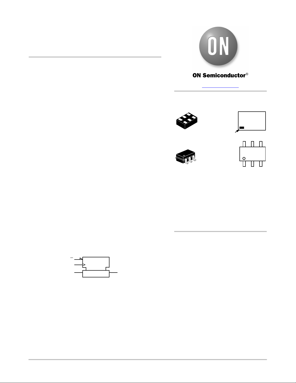
TinyLogic UHS D-Type
Flip-Flop with
Asynchronous Clear
NC7SZ175
Description
The NC7SZ175 is a single positive edge−triggered D−type CMOS
Flip−Flop with Asynchronous Clear from ON Semiconductor’s Ultra
High Speed Series of TinyLogic in the space saving SC70 6−lead
package. The device is fabricated with advanced CMOS technology to
achieve ultra high speed with high output drive while maintaining low
static power dissipation over a very broad V
device is specified to operate over the 1.65 V to 5.5 V V
inputs and output are high impedance when V
voltages up to 5.5 V independent of V
operating range. The
CC
range. The
CC
is 0 V. Inputs tolerate
CC
operating voltage. This
CC
single flip−flop will store the state of the D input that meets the setup
and hold time requirements on the LOW−to−HIGH Clock (CP)
transition. A LOW input to Clear sets the Q output to LOW level. The
Clear input is independent of clock.
Features
• Space Saving SC−88 6−Lead Package
• Ultra Small MicroPak™ Leadless Package
• Ultra High Speed: t
• High Output Drive: ±24 mA at 3 V V
• Broad V
Operating Range: 1.65 V to 5.5 V
CC
• Matches the Performance of LCX when Operated at 3.3 V V
= 2.6 ns Typ into 50 pF at 5 V V
PD
CC
CC
CC
• Power Down High Impedance Inputs / Output
• Overvoltage Tolerant Inputs Facilitate 5 V to 3 V Translation
• Proprietary Noise / EMI Reduction Circuitry Implemented
• These Devices are Pb−Free, Halogen Free/BFR Free and are RoHS
Compliant
IEEC / IEC
C
CP
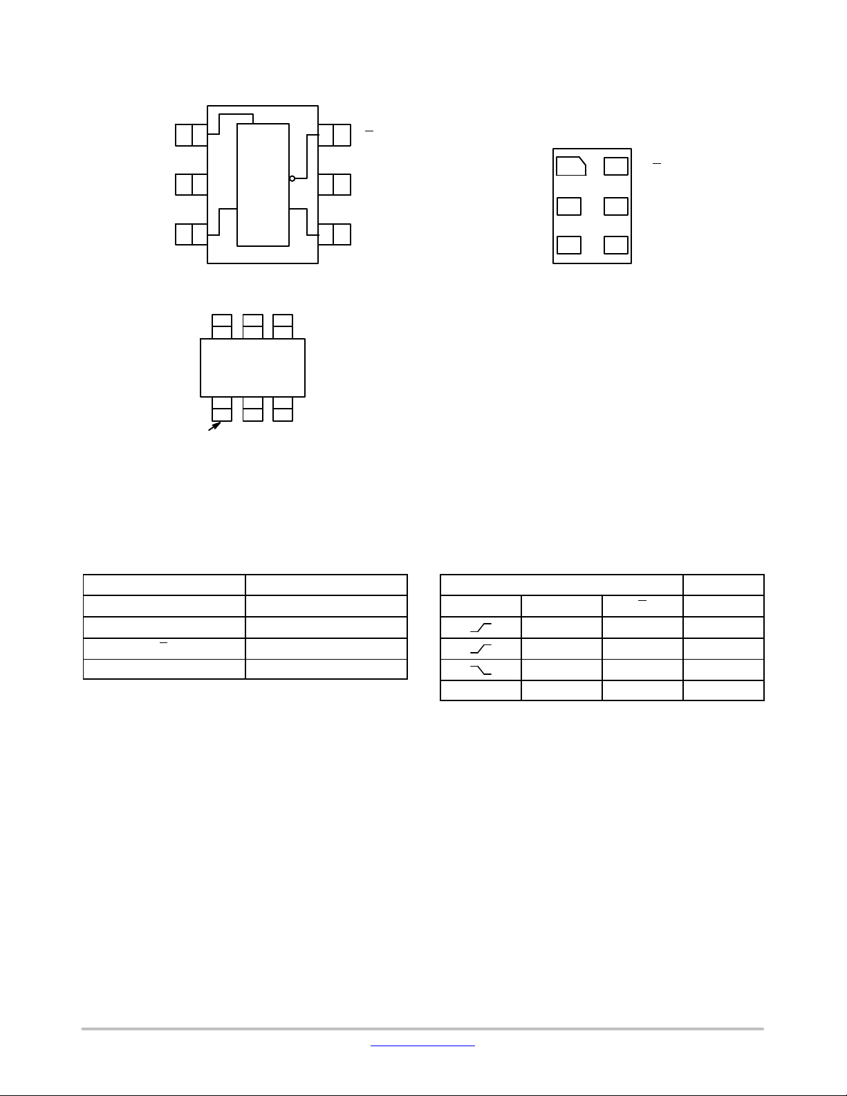
www.onsemi.com
MARKING
DIAGRAMS
SIP6 1.45x1.0
CASE 127EB
Pin 1
SC−88
CASE 419B−02
C4, Z75 = Specific Device Code
KK = 2−Digit Lot Run Traceability Code
XY = 2−Digit Date Code Format
Z = Assembly Plant Code
M = Date Code*
G = Pb−Free Package
(Note: Microdot may be in either location)
*Date Code orientation and/or position may
vary depending upon manufacturing location.
ORDERING INFORMATION
See detailed ordering, marking and shipping information in the
package dimensions section on page 6 of this data sheet.
C4KK
XYZ
6
G
Z75M
G
1
D
Figure 1. Logic Symbol
© Semiconductor Components Industries, LLC, 2004
January, 2021 − Rev. 4
Q
1 Publication Order Number:
NC7SZ175/D
Connection Diagrams
NC7SZ175
CP C
1
GND V
2
DQ
3
CP
C
D Q
6
5
CC
4
Figure 2. SC70 (Top View)
(Top View) AAA
Pin One
AAA represents Product Code Top Mark − see ordering code.
NOTE: Orientation of Top Mark determines Pin One location.
Read the Top Product Code Mark left to right, Pin One
is the lower left pin (see diagram).
Figure 3. Pin 1 Orientation
CP 1 6 C
GND 2 5 V
D 3 4 Q
CC
Figure 4. MicroPak (Top Through View)
PIN DESCRIPTIONS
Pin Name Description
D Data Input
CP Clock Pulse Input
C Clear Input
Q Flip−Flop Output
FUNCTION TABLE
Inputs Output
CP D C Q
L H L
H H H
X H Qn
X X L L
H = HIGH Logic Level Qn = No Change in Data
L = LOW Logic Level X = Immaterial
www.onsemi.com
2
NC7SZ175
ABSOLUTE MAXIMUM RATINGS
Symbol Parameter Min Max Unit
V
CC
V
IN
V
OUT
I
IK
I
OK
I
OUT
ICC / I
T
STG
T
J
T
L
P
D
Stresses exceeding those listed in the Maximum Ratings table may damage the device. If any of these limits are exceeded, device functionality
should not be assumed, damage may occur and reliability may be affected.
RECOMMENDED OPERATING CONDITIONS
Symbol Parameter Conditions Min Max Unit
V
CC
V
IN
V
OUT
tr, t
f
T
A
q
JA
Functional operation above the stresses listed in the Recommended Operating Ranges is not implied. Extended exposure to stresses beyond
the Recommended Operating Ranges limits may affect device reliability.
1. Unused inputs must be held HIGH or LOW. They may not float.
Supply Voltage −0.5 +6.5 V
DC Input Voltage −0.5 +6.5 V
DC Output Voltage −0.5 +6.5 V
DC Input Diode Current VIN < 0 V − −50 mA
DC Output Diode Current V
< 0 V − −50 mA
OUT
DC Output Source / Sink Current − ±50 mA
DC VCC / GND Current − ±50 mA
GND
Storage Temperature Range −65 +150 °C
Junction Temperature under Bias − 150 °C
Junction Lead Temperature (Soldering, 10 Seconds) − 260 °C
Power Dissipation in Still Air
SC−88 − 332
MicroPak−6 − 812
Supply Voltage Operating 1.65 5.5
Supply Voltage Data Retention 1.5 5.5
Input Voltage 0 5.5 V
Output Voltage 0 V
Input Rise and Fall Time
VCC = 1.8 V, 2.5 V ±0.2 V 0 20
CC
VCC = 3.3 V ±0.3 V 0 10
V
= 5.5 V ±0.5 V 0 5
CC
Operating Temperature −40 +85 °C
Thermal Resistance
SC−88 − 377
MicroPak−6 − 154
mW
V
V
ns/V
°C/W
www.onsemi.com
3
 Loading...