ON Semiconductor NC7S04 User Manual

TinyLogic HS Inverter
NC7S04
Description
The NC7S04 is a single high performance CMOS Inverter.
Advanced Silicon Gate CMOS fabrication assures high speed and low
power circuit operation over a broad V
diodes inherently guard both input and output with respect to the V
and GND rails. Three stages of gain between input and output assures
high noise immunity and reduced sensitivity to input edge rate.
Features
• Space−Saving SC−74A and SC−88A 5−Lead Package
• Ultra−Small MicroPak™ Leadless Package
• High Speed: t
• Low Quiescent Power: I
• Balanced Output Drive: 2 mA I
• Broad V
CC
= 3 ns Typ
PD
< 1 mA
CC
, −2 mA I
OL
Operating Range: 2 V – 6 V
• Balanced Propagation Delays
• Specified for 3 V Operation
• These Devices are Pb−Free, Halogen Free/BFR Free and are RoHS
Compliant
range. ESD protection
CC
OH
CC
www.onsemi.com
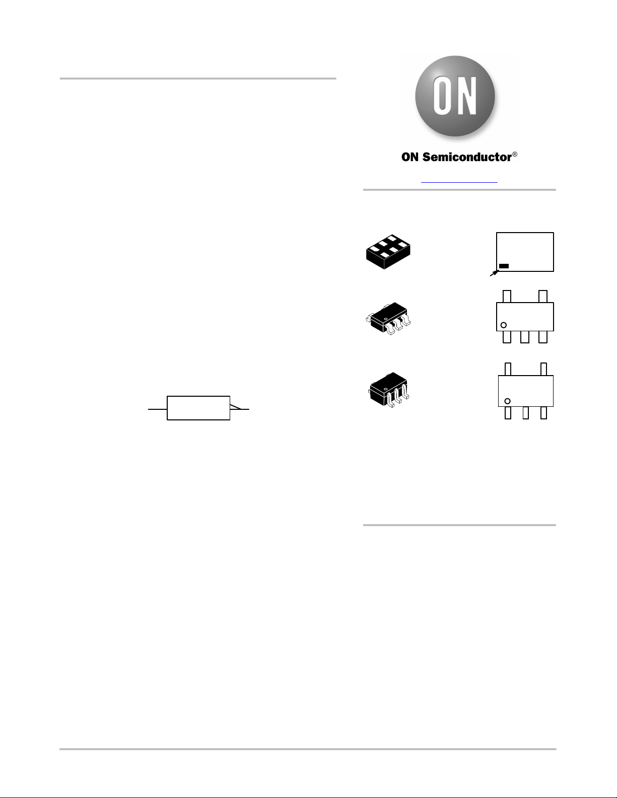
SIP6
CASE 127EB
Pin 1
SC−74A
CASE 318BQ
MARKING
DIAGRAMS
AAKK
XYZ
7S04MG
G
IEEE / IEC
1
Figure 1. Logic Symbol
SC−88A
CASE 419A−02
YA
AA, 7S04, S04 = Specific Device Code
KK = 2−Digit Lot Run Traceability Code
XY = 2−Digit Date Code Format
Z = Assembly Plant Code
M = Date Code*
*Date Code orientation and/or position may
vary depending upon manufacturing location.
ORDERING INFORMATION
See detailed ordering, marking and shipping information in the
package dimensions section on page 5 of this data sheet.
S04MG
G
© Semiconductor Components Industries, LLC, 2004
January, 2021 − Rev. 2
1 Publication Order Number:
NC7S04/D

Pin Configurations
NC7S04
NC
A
GND Y
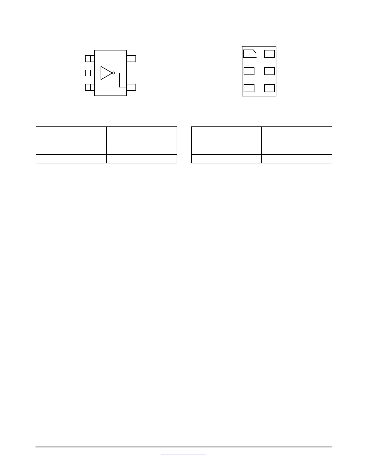
Figure 2. SC−88A and SC−74A (Top View)
PIN DESCRIPTIONS
Name Description
A Input
Y Output
NC No Connect
1
2
3
5
V
CC
4
NC 1 6 V
A 2 5 NC
GND 3 4 Y
CC
Figure 3. MicroPak (Top Through View)
FUNCTION TABLE (Y = A)
Input
A Y
L H
H L
H = HIGH Logic Level
L = LOW Logic Level
Output
www.onsemi.com
2

NC7S04
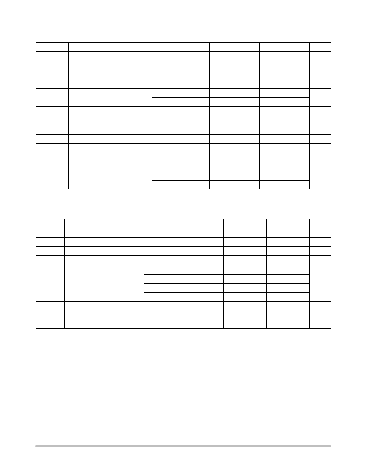
ABSOLUTE MAXIMUM RATINGS
Symbol Parameter Min Max Unit
V
CC
I
IK
V
IN
I
OK
V
OUT
I
OUT
ICC or I
T
STG
T
J
T
L
P
D
Stresses exceeding those listed in the Maximum Ratings table may damage the device. If any of these limits are exceeded, device functionality
should not be assumed, damage may occur and reliability may be affected.
Supply Voltage −0.5 6.5 V
DC Input Diode Current
DC Input Voltage −0.5 V
DC Output Diode Current
DC Output Voltage −0.5 V
VIN < 0 V − −20
VIN > V
CC
V
< 0 V − −20
OUT
V
> V
OUT
CC
− +20
CC
− +20
CC
+ 0.5 V
+ 0.5 V
DC Output Source or Sink Current − ±12.5 mA
DC VCC or Ground Current per Output Pin − ±25 mA
GND
Storage Temperature −65 +150 °C
Junction Temperature − +150 °C
Lead Temperature (Soldering, 10 Seconds) − +260 °C
Power Dissipation in Still Air
SC−74A − 390
SC−88A − 332
MicroPak−6 − 812
mA
mA
mW
RECOMMENDED OPERATING CONDITIONS
Symbol Parameter Conditions Min Max Unit
V
CC
V
IN
V
OUT
T
tr, t
q
JA
Functional operation above the stresses listed in the Recommended Operating Ranges is not implied. Extended exposure to stresses beyond
the Recommended Operating Ranges limits may affect device reliability.
1. Unused inputs must be held HIGH or LOW. They may not float.
Supply Voltage 2.0 6.0 V
Input Voltage 0 V
Output Voltage 0 V
Operating Temperature −40 +85 °C
A
Input Rise and Fall Times
f
VCC at 2.0 V 0 20
VCC at 3.0 V 0 20
VCC at 4.5 V 0 10
VCC at 6.0 V 0 5
Thermal Resistance
SC−74A − 320
SC−88A − 377
MicroPak−6 − 154
CC
CC
V
V
ns
°C/W
www.onsemi.com
3
 Loading...