

NB6N11S
3.3 V 1:2 AnyLevelE Input
to LVDS Fanout Buffer /
Translator
Description
The NB6N11S is a differential 1:2 Clock or Data Receiver and will
accept AnyLevel input signals: LVPECL, CML, LVCMOS, LVTTL,
or LVDS. These signals will be translated to LVDS and two identical
copies of Cloc k o r D a t a will be distributed, operating up to 2.0 GHz or
2.5 Gb/s, respectively. As such, the NB6N11S is ideal for SONET,
GigE, Fiber Channel, Backplane and other Clock or Data distribution
applications.
The NB6N11S has a wide input common mode range from
GND + 50 mV to V
termination resistors at the inputs, the NB6N11S is ideal for
translating a variety of differential or single−ended Clock or Data
signals to 350 mV typical LVDS output levels.
The NB6N11S is functionally equivalent to the EP11, LVEP11,
SG11 or 7L11M devices and is offered in a small, 3 mm X 3 mm,
16−QFN package. Application notes, models, and support
documentation are available at www.onsemi.com
The NB6N11S is a member of the ECLinPS MAX™ family of high
performance products.
Features
• Maximum Input Clock Frequency > 2.0 GHz
• Maximum Input Data Rate > 2.5 Gb/s
• 1 ps Maximum of RMS Clock Jitter
• Typically 10 ps of Data Dependent Jitter
• 380 ps Typical Propagation Delay
• 120 ps Typical Rise and Fall Times
• Functionally Compatible with Existing 3.3 V LVEL, LVEP, EP, and
SG Devices
• These are Pb−Free Devices
− 50 mV. Combined with the 50 W internal
CC
.
http://onsemi.com
MARKING
DIAGRAM*
16
1
1
QFN−16
MN SUFFIX
CASE 485G
A = Assembly Location
L = Wafer Lot
Y = Year
W = Work Week
G = Pb−Free Package
(Note: Microdot may be in either location)
*For additional marking information, refer to
Application Note AND8002/D.
V
TD
D
D
NB6N
11S
ALYWG
G
Q0
Q0
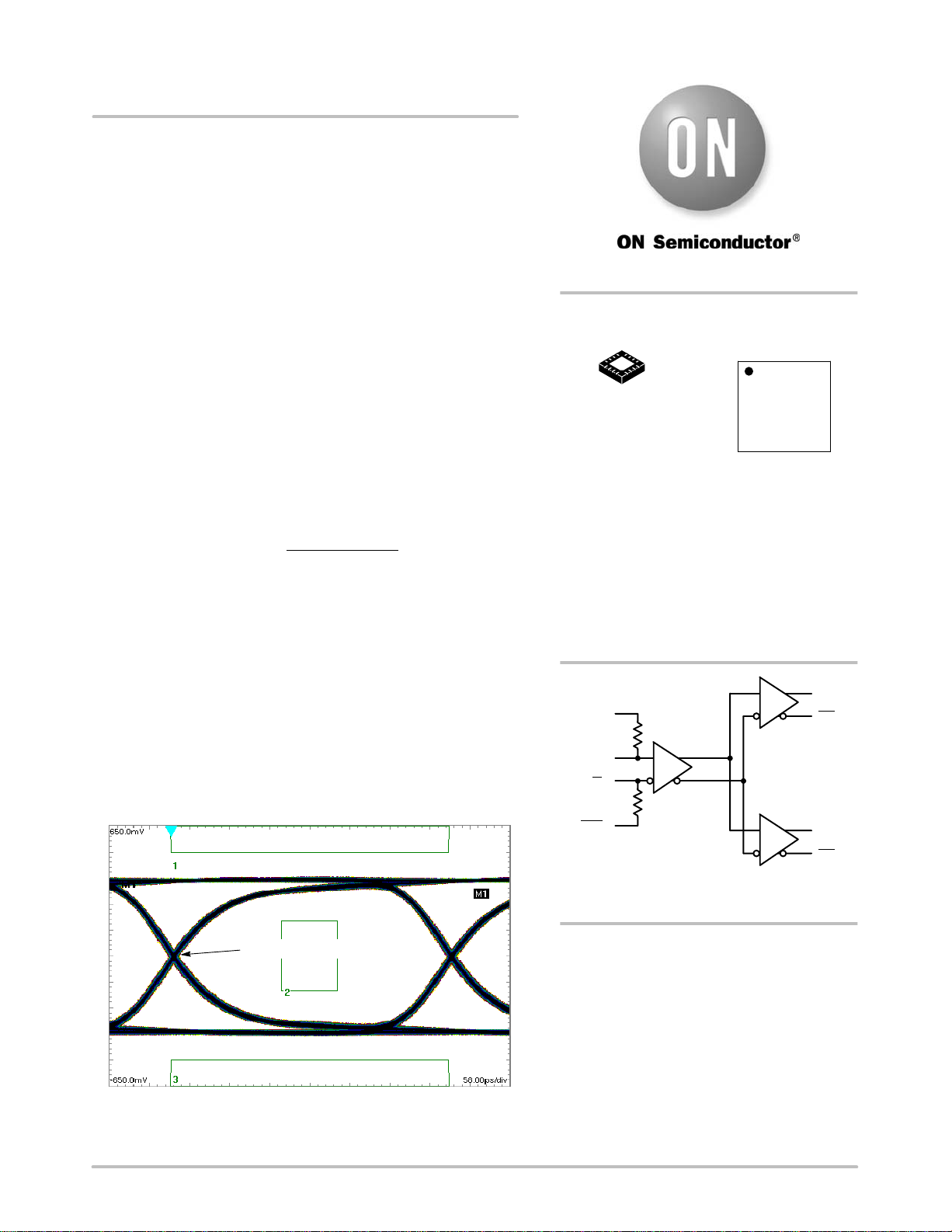
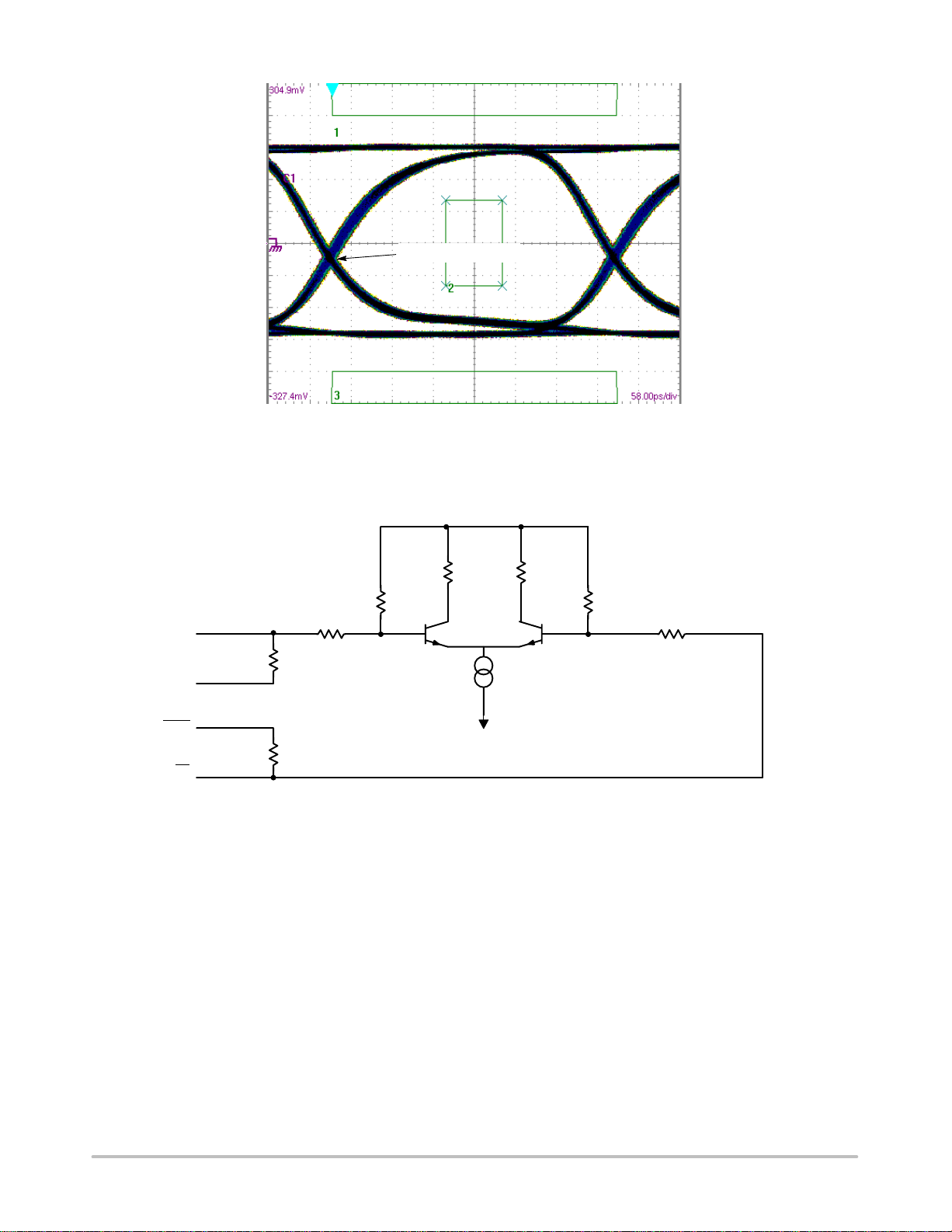
Device DDJ = 10 ps
VOLTAGE (130 mV/div)
TIME (58 ps/div)
Figure 2. Typical Output Waveform at 2.488 Gb/s with
PRBS 2
© Semiconductor Components Industries, LLC, 2007
April, 2007 − Rev. 1
23−1
(V
= 400 mV; Input Signal DDJ = 14 ps)
INPP
V
TD
Figure 1. Logic Diagram
ORDERING INFORMATION
See detailed ordering and shipping information in the package
dimensions section on page 8 of this data sheet.
1 Publication Order Number:
Q1
Q1
NB6N11S/D
NB6N11S
Exposed Pad (EP)
VCCVCCV
CC
V
CC
16 15 14 13
Q0
Q0
1
2
12
11
V
TD
D
NB6N11S
Q1
Q1
3
4
10
D
V
9
TD
5678
V
NC VEEV
CC
EE
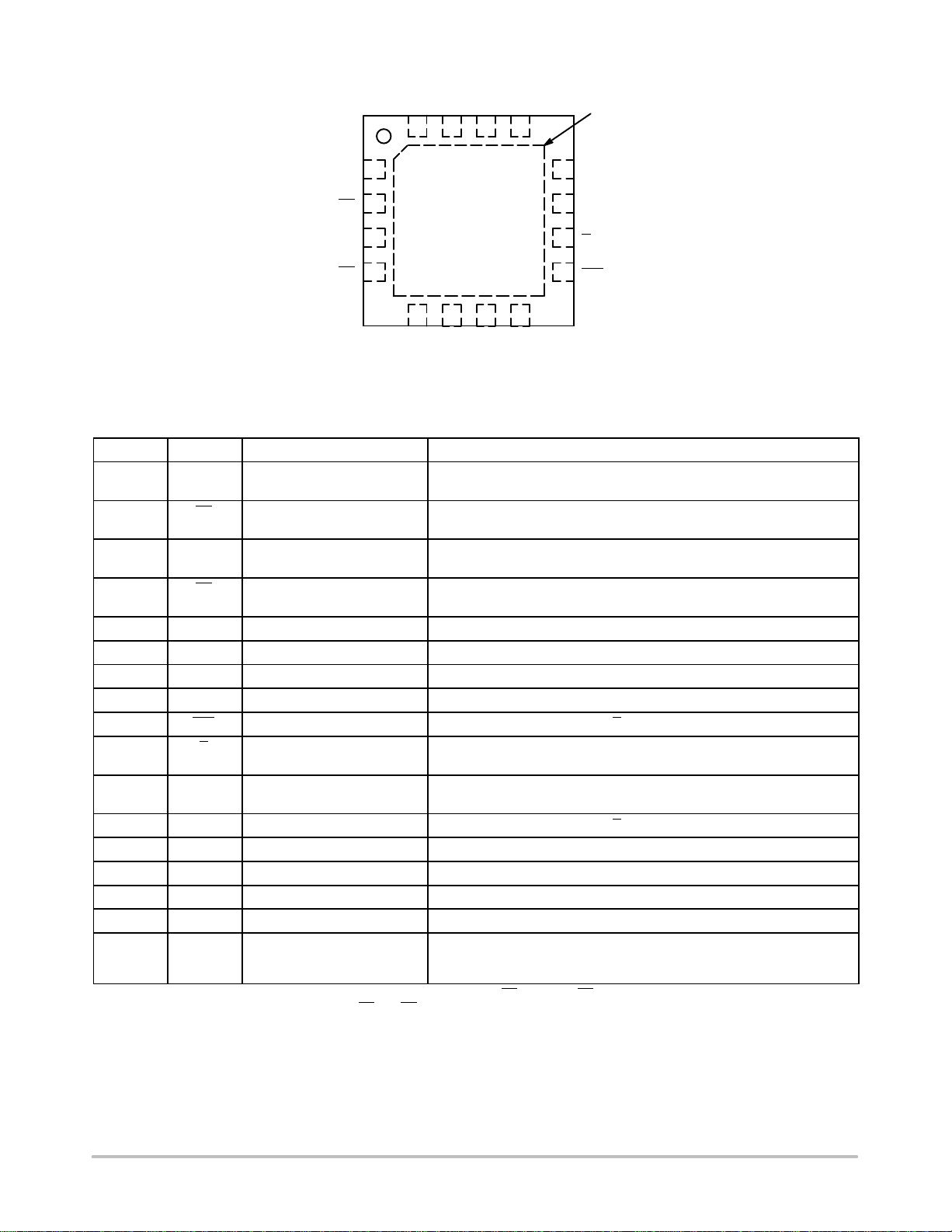
Figure 3. NB6N11S Pinout, 16−pin QFN (Top View)
Table 1. PIN DESCRIPTION
Pin Name I/O Description
1 Q0 LVDS Output
2 Q0 LVDS Output
3 Q1 LVDS Output
4 Q1 LVDS Output
5 V
CC
− Positive Supply Voltage
6 NC No Connect
7 V
8 V
9 V
EE
EE
TD
−
10 D LVPECL, CML, LVDS,
LVCMOS, LVTTL
11 D LVPECL, CML, LVDS,
LVCMOS, LVTTL
12 V
13 V
14 V
15 V
16 V
TD
CC
CC
CC
CC
−
− Positive Supply Voltage
− Positive Supply Voltage
− Positive Supply Voltage
− Positive Supply Voltage
EP Exposed pad. The exposed pad (EP) on the package bottom must be
1. In the differential configuration when the input termination pins(VTD0/VTD0, VTD1/ VTD1) are connected to a common termination voltage
or left open, and if no signal is applied on D0/D0
, D1/D1 input, then the device will be susceptible to self−oscillation.
Non−inverted D output. Typically loaded with 100 W receiver termination
resistor across differential pair.
Inverted D output. Typically loaded with 10 W receiver termination resistor
across differential pair.
Non−inverted D output. Typically loaded with 100 W receiver termination
resistor across differential pair.
Inverted D output. Typically loaded with 100 W receiver termination resistor
across differential pair.
Negative Supply Voltage
Negative Supply Voltage
Internal 50 W termination pin for D
Inverted Differential Clock/Data Input (Note 1)
Non−inverted Differential Clock/Data Input (Note 1)
Internal 50 W termination pin for D
attached to a heat−sinking conduit. The exposed pad may only be
electrically connected to V
EE
.
http://onsemi.com
2
NB6N11S
Table 2. ATTRIBUTES
Characteristics Value
ESD Protection Human Body Model
Machine Model
Charged Device Model
Moisture Sensitivity, Indefinite Time Out of Drypack (Note 2) Pb Pkg Pb−Free Pkg
QFN−16 − 1
Flammability Rating Oxygen Index: 28 to 34 UL 94 V−0 @ 0.125 in
Transistor Count 225 Devices
Meets or exceeds JEDEC Spec EIA/JESD78 IC Latchup Test
2. For additional information, see Application Note AND8003/D.
Table 3. MAXIMUM RATINGS
Symbol Parameter Condition 1 Condition 2 Rating Unit
V
CC
V
IN
I
IN
I
OSC
T
A
T
stg
q
JA
q
JC
T
sol
Stresses exceeding Maximum Ratings may damage the device. Maximum Ratings are stress ratings only. Functional operation above the
Recommended Opera t i n g Conditions is not implied. Extended exposure to stresses above the Recommended Operating Conditions may affect
device reliability.
3. JEDEC standard multilayer board − 1S2P (1 signal, 2 power) with 8 filled thermal vias under exposed pad.
Positive Power Supply GND = 0 V 3.8 V
Positive Input GND = 0 V VIN ≤ V
Input Current Through R
(50 W Resistor)
T
Static
Surge
Output Short Circuit Current
Line−to−Line (Q to Q
Line−to−End (Q or Q to GND)
)
Q or Q to GND
Q to Q
Operating Temperature Range QFN−16 −40 to +85 °C
Storage Temperature Range −65 to +150 °C
Thermal Resistance (Junction−to−Ambient) (Note 3) 0 lfpm
500 lfpm
Thermal Resistance (Junction−to−Case) 1S2P (Note 3) QFN−16 4.0 °C/W
Wave Solder Pb
Pb−Free
> 2 kV
> 200 V
> 1 kV
CC
Continuous
Continuous
QFN−16
QFN−16
3.8 V
35
70
12
24
41.6
35.2
265
265
mA
mA
mA
°C/W
°C/W
°C
http://onsemi.com
3
NB6N11S
Table 4. DC CHARACTERISTICS, CLOCK INPUTS, LVDS OUTPUTS V
Symbol
I
CC
Power Supply Current (Note 8) 35 50 mA
Characteristic Min Typ Max Unit
= 3.0 V to 3.6 V, GND = 0 V, TA = −40°C to +85°C
CC
DIFFERENTIAL INPUTS DRIVEN SINGLE−ENDED (Figures 11, 12, 16, and 18)
V
th
V
IH
V
IL
Input Threshold Reference Voltage Range (Note 7) GND +100 VCC − 100 mV
Single−ended Input HIGH Voltage Vth + 100 V
CC
Single−ended Input LOW Voltage GND Vth − 100 mV
DIFFERENTIAL INPUTS DRIVEN DIFFERENTIALLY (Figures 7, 8, 9, 10, 17, and 19)
V
V
V
V
R
IHD
ILD
CMR
ID
TIN
Differential Input HIGH Voltage 100 V
CC
Differential Input LOW Voltage GND VCC − 100 mV
Input Common Mode Range (Differential Configuration) GND + 50 VCC − 50 mV
Differential Input Voltage (V
IHD
− V
) 100 V
ILD
CC
Internal Input Termination Resistor 40 50 60
LVDS OUTPUTS (Note 4)
V
DV
V
DV
V
V
OD
OS
OH
OL
Differential Output Voltage 250 450 mV
Change in Magnitude of VOD for Complementary Output States (Note 9) 0 1 25 mV
OD
Offset Voltage (Figure 15) 1125 1375 mV
Change in Magnitude of VOS for Complementary Output States (Note 9) 0 1 25 mV
OS
Output HIGH Voltage (Note 5) 1425 1600 mV
Output LOW Voltage (Note 6) 900 1075 mV
NOTE: Device will meet the specifications after thermal equilibrium has been established when mounted in a test socket or printed circuit
board with maintained transverse airflow greater than 500 lfpm. Electrical parameters are guaranteed only over the declared
operating temperature range. Functional operation of the device exceeding these conditions is not implied. Device specification limit
values are applied individually under normal operating conditions and not valid simultaneously.
4. LVDS outputs require 100 W receiver termination resistor between differential pair. See Figure 14.
5. V
max = VOSmax + ½ VODmax.
OH
6. V
max = VOSmin − ½ VODmax.
OL
is applied to the complementary input when operating in single−ended mode.
7. V
th
8. Input termination pins open, D/D
9. Parameter guaranteed by design verification not tested in production.
at the DC level within V
and output pins loaded with RL = 100 W across differential.
CMR
mV
mV
mV
W
http://onsemi.com
4
NB6N11S
l
t
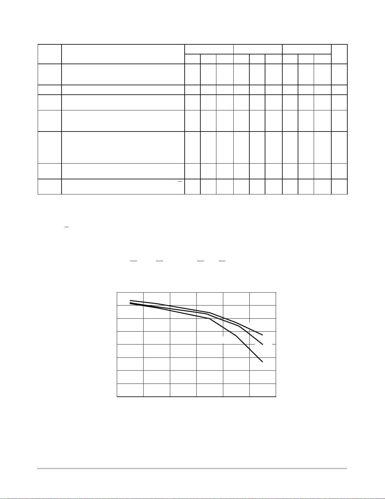
Table 5. AC CHARACTERISTICS V
= 3.0 V to 3.6 V, GND = 0 V; (Note 10)
CC
−40°C 25°C 85°C
Symbo
V
OUTPP
f
DATA
t
,
PLH
t
PHL
t
SKEW
t
JITTER
V
INPP
t
r
t
f
Characteristic
Output Voltage Amplitude (@ V
(Figure 4) fin= 1.5 GHz
INPPmin)fin
≤ 1.0 GHz
fin= 2.0 GHz
Maximum Operating Data Rate 1.5 2.5 1.5 2.5 1.5 2.5 Gb/s
Differential Input to Differential Output
Propagation Delay
Duty Cycle Skew (Note 11)
Within Device Skew (Note 16)
Device−to−Device Skew (Note 15)
RMS Random Clock Jitter (Note 13) fin = 1.0 GHz
f
= 1.5 GHz
Deterministic Jitter (Note 14) f
= 622 Mb/s
DATA
= 1.5 Gb/s
f
DATA
f
= 2.488 Gb/s
DATA
in
Input Voltage Swing/Sensitivity
(Differential Configuration) (Note 12)
Output Rise/Fall Times @ 250 MHz Q, Q
(20% − 80%)
Min Typ Max Min Typ Max Min Typ Max
220
200
170
350
300
270
250
200
170
350
300
270
250
200
170
350
300
270
Uni
270 370 470 270 370 470 270 370 470 ps
8
45
5
25
30
100
0.5
1
0.5
1
6
7
20
10
20
100 VCC−
GND
8
45
5
25
30
100
0.5
1
0.5
1
6
7
20
10
20
100 VCC−
GND
8
45
5
25
30
100
0.5
1
0.5
1
6
7
20
10
20
100 VCC−
GND
70 120 170 70 120 170 70 120 170 ps
NOTE: Device will meet the specifications after thermal equilibrium has been established when mounted in a test socket or printed circuit
board with maintained transverse airflow greater than 500 lfpm. Electrical parameters are guaranteed only over the declared
operating temperature range. Functional operation of the device exceeding these conditions is not implied. Device specification limit
values are applied individually under normal operating conditions and not valid simultaneously.
10.Measured by forcing V
“D” and “D
” of the receiver. Input edge rates 150 ps (20%−80%).
11.See Figure 13 differential measurement of t
12.Input voltage swing is a single−ended measurement operating in differential mode.
13.RMS jitter with 50% Duty Cycle clock signal at 750 MHz.
14.Deterministic jitter with input NRZ data at PRBS 2
with 50% duty cycle clock source and VCC − 1400 mV offset. All loading with an external RL = 100 W across
INPPmin
= |t
− t
skew
PLH
23
−1 and K28.5.
| for a nominal 50% differential clock input waveform @ 250 MHz.
PHL
15.Skew is measured between outputs under identical transition @ 250 MHz.
16.The worst case condition between Q0/Q0
and Q1/Q1 from either D0/D0 or D1/D1, when both outputs have the same transition.
mV
ps
ps
mV
400
350
300
250
200
150
100
50
OUTPUT VOLTAGE AMPLITUDE (mV)
0
0.5 1 1.5 2 2.5 30
Figure 4. Output Voltage Amplitude (V
Input Clock Frequency (f
85°C
INPUT CLOCK FREQUENCY (GHz)
) and Temperature (@ VCC = 3.3 V)
in
OUTPP
http://onsemi.com
5
−40°C
25°C
) versus
VOLTAGE (63.23 mV/div)
NB6N11S
Device DDJ = 10 ps
TIME (58 ps/div)
Figure 5. Typical Output Waveform at 2.488 Gb/s with PRBS 2
(V
= 100 mV; Input Signal DDJ = 14 ps)
INPP
R
C
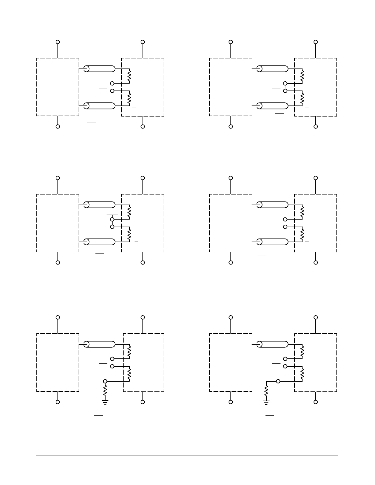
Dx
50 W
V
TDx
V
TDx
50 W
D
x
I
Figure 6. Input Structure
23−1
and OC48 mask
R
C
1.25 kW1.25 kW
1.25 kW1.25 kW
http://onsemi.com
6
NB6N11S
V
V
V
V
TIN
CC
Zo = 50 W
LVPECL
Driver
V
TD
V
TD
Zo = 50 W
CC
NB4N11S
D
50 W*
50 W*
D
CC
CC
NB4N11S
Zo = 50 W
LVDS
Driver
V
TD
V
TD
Zo = 50 W
VTD = V
TD
D
50 W*
50 W*
D
VTD = VTD = VCC − 2.0 V
GND
Figure 7. LVPECL Interface
V
CC
Zo = 50 W
CML
Driver
V
V
TD
TD
V
CC
GND
V
CC
NB4N11S
D
50 W*
50 W*
GND
Figure 8. LVDS Interface
V
CC
Zo = 50 W
HSTL
Driver
GND
V
CC
NB4N11S
D
50 W*
V
TD
V
TD
50 W*
GND
Zo = 50 W
VTD = VTD = V
CC
D
GND
Figure 9. Standard 50 W Load CML Interface
V
CC
LVCMOS
Driver
GND
Zo = 50 W
V
TD
V
TD
2.5 kW
GND
VTD = VTD = OPEN
V
CC
NB4N11S
D
50 W*
50 W*
D
GND
Figure 11. LVCMOS Interface
Zo = 50 W
VTD = VTD = GND or VDD/2
GND
Depending on Driver.
Figure 10. HSTL Interface
V
CC
Zo = 50 W
LVTTL
Driver
GND
GND
= VTD = OPEN
V
TD
Figure 12. LVTTL Interface
V
TD
V
TD
1.5 kW
D
GND
V
CC
NB4N11S
D
50 W*
50 W*
D
GND
*R
, Internal Input Termination Resistor.
http://onsemi.com
7

NB6N11S
D
V
= VIH(D) − VIL(D)
INPP
D
Q
V
= VOH(Q) − VOL(Q)
OUTPP
Q
t
PHL
t
PLH
Figure 13. AC Reference Measurement
LVDS
Driver
Device
QD
Q D
Zo = 50 W
Zo = 50 W
100 W
LVDS
Receiver
Device
Figure 14. Typical LVDS Termination for Output Driver and Device Evaluation
Q
N
V
OS
Q
N
V
OH
V
OD
V
OL
Figure 15. LVDS Output
D
V
IH
V
th
V
IL
D
D
D
V
th
Figure 16. Differential Input Driven Single−Ended
V
V
V
th
V
CC
thmax
thmin
GND
D
D
V
IHmax
V
ILmax
V
IHmin
V
ILmin
Figure 18. Vth Diagram
Figure 17. Differential Inputs Driven Differentially
V
CC
V
GND
CMR
Figure 19. V
CMR
V
IH(MAX)
V
IL
V
IH
V
= V
INPP
V
IL
V
IH
V
IL(MIN)
Diagram
IHD
− V
ILD
ORDERING INFORMATION
Device Package Shipping
NB6N11SMNG QFN−16, 3 X 3 mm
123 Units / Rail
(Pb−Free)
NB6N11SMNR2G QFN−16, 3 X 3 mm
3000 / Tape & Reel
(Pb−Free)
†For information on tape and reel specifications, including part orientation and tape sizes, please refer to our Tape and Reel Packaging
Specifications Brochure, BRD8011/D.
†
http://onsemi.com
8

16 X
LOCATION
0.10 C
0.08 C
16X
NOTE 5
PIN 1
0.15 C
0.15
L
D
TOP VIEW
C
SIDE VIEW
D2
58
NB6N11S
PACKAGE DIMENSIONS
16 PIN QFN
CASE 485G−01
ISSUE C
A
B
E
(A3)
A
SEATING
A1
e
EXPOSED PAD
PLANE
C
0.575
0.022
NOTES:
1. DIMENSIONING AND TOLERANCING PER
ASME Y14.5M, 1994.
2. CONTROLLING DIMENSION: MILLIMETERS.
3. DIMENSION b APPLIES TO PLATED
TERMINAL AND IS MEASURED BETWEEN
0.25 AND 0.30 MM FROM TERMINAL.
4. COPLANARITY APPLIES TO THE EXPOSED
PAD AS WELL AS THE TERMINALS.
CONDITION CAN NOT VIOLATE 0.2 MM
5. L
max
MINIMUM SPACING BETWEEN LEAD TIP
AND FLAG
MILLIMETERS
DIM MIN MAX
A 0.80 1.00
A1 0.00 0.05
A3 0.20 REF
b 0.18 0.30
D 3.00 BSC
D2 1.65 1.85
E 3.00 BSC
E2 1.65 1.85
e 0.50 BSC
K
0.18 TYP
L 0.30 0.50
SOLDERING FOOTPRINT*
3.25
0.128
0.30
0.012
EXPOSED PAD
16X
0.10 C
0.05
K
C
16X
A B
NOTE 3
4
1
16 13
b
BOTTOM VIEW
9
E2
e
12
3.25
0.128
1.50
0.059
0.30
0.50
0.02
0.012
SCALE 10:1
ǒ
inches
*For additional information on our Pb−Free strategy and soldering
details, please download the ON Semiconductor Soldering and
Mounting Techniques Reference Manual, SOLDERRM/D.
AnyLevel and ECLinPS MAX are trademarks of Semiconductor Components Industries, LLC (SCILLC).
ON Semiconductor and are registered trademarks of Semiconductor Components Industries, LLC (SCILLC). SCILLC reserves the right to make changes without further notice
to any products herein. SCILLC makes no warranty, representation or guarantee regarding the suitability of its products for any particular purpose, nor does SCILLC assume any liability
arising out of the application or use of any product or circuit, and specifically disclaims any and all liability, including without limitation special, consequential or incidental damages.
“Typical” parameters which may be provided in SCILLC data sheets and/or specifications can and do vary in different applications and actual performance may vary over time. All
operating parameters, including “Typicals” must be validated for each customer application by customer’s technical experts. SCILLC does not convey any license under its patent rights
nor the rights of others. SCILLC products are not designed, intended, or authorized for use as components in systems intended for surgical implant into the body, or other applications
intended to support or sustain life, or for any other application in which the failure of the SCILLC product could create a situation where personal injury or death may occur. Should
Buyer purchase or use SCILLC products for any such unintended or unauthorized application, Buyer shall indemnify and hold SCILLC and its officers, employees, subsidiaries, affiliates,
and distributors harmless against all claims, costs, damages, and expenses, and reasonable attorney fees arising out of, directly or indirectly, any claim of personal injury or death
associated with such unintended or unauthorized use, even if such claim alleges that SCILLC was negligent regarding the design or manufacture of the part. SCILLC is an Equal
Opportunity/Affirmative Action Employer. This literature is subject to all applicable copyright laws and is not for resale in any manner.
mm
Ǔ
PUBLICATION ORDERING INFORMATION
LITERATURE FULFILLMENT:
Literature Distribution Center for ON Semiconductor
P.O. Box 5163, Denver, Colorado 80217 USA
Phone: 303−675−2175 or 800−344−3860 Toll Free USA/Canada
Fax: 303−675−2176 or 800−344−3867 Toll Free USA/Canada
Email: orderlit@onsemi.com
N. American Technical Support: 800−282−9855 Toll Free
USA/Canada
Europe, Middle East and Africa Technical Support:
Phone: 421 33 790 2910
Japan Customer Focus Center
Phone: 81−3−5773−3850
http://onsemi.com
9
ON Semiconductor Website: www.onsemi.com
Order Literature: http://www.onsemi.com/orderlit
For additional information, please contact your local
Sales Representative
NB6N11S/D
 Loading...