

Page 1

NB6L295M
2.5V / 3.3V Dual Channel
Programmable Clock/Data
Delay with Differential CML
Outputs
Multi−Level Inputs w/ Internal Termination
The NB6L295M is a Dual Channel Programmable Delay Chip
designed primarily for Clock or Data de−skewing and timing
adjustment. The NB6L295M is versatile in that two individual
variable delay channels, PD0 and PD1, can be configured in one of
two operating modes, a Dual Delay or an Extended Delay.
In the Dual Delay Mode, each channel has a programmable delay
section which is designed using a matrix of gates and a chain of
multiplexers. There is a fixed minimum delay of 3.2 ns per channel.
The Extended Delay Mode amounts to the additive delay of PD0
plus PD1 and is accomplished with the Serial Data Interface MSEL bit
set High. This will internally cascade the output of PD0 into the input
of PD1. Therefore, the Extended Delay path starts at the IN0/IN0
inputs, flows through PD0, cascades to the PD1 and outputs through
Q1/Q1
. There is a fixed minimum delay of 6.0 ns for the Extended
Delay Mode.
The required delay is accomplished by programming each delay
channel via a 3−pin Serial Data Interface, described in the application
section. The digitally selectable delay has an increment resolution of
typically 11 ps with a net programmable delay range of either 0 ns to
6 ns per channel in Dual Delay Mode; or from 0 ns to 11.2 ns for the
Extended Delay Mode.
The Multi−Level Inputs can be driven directly by differential
LVPECL, LVDS or CML logic levels; or by single ended LVPECL,
LVCMOS or LVTTL. A single enable pin is available to control both
inputs. The SDI input pins are controlled by LVCMOS or LVTTL
level signals. The NB6L295M 16 mA CML output contains
temperature compensation circuitry. This device is offered in a 4 mm x
4 mm 24−pin QFN Pb−free package. The NB6L295M is a member of
the ECLinPS MAX™ family of high performance products.
Features
• Input Clock Frequency > 1.5 GHz with 210 mV
V
OUTPP
• Input Data Rate > 2.5 Gb/s
• Programmable Delay Range: 0 ns to 6 ns per Delay
Channel
• Programmable Delay Range: 0 ns to 11.2 ns for
Extended Delay Mode
• Total Delay Range: 3.2 ns to 8.5 ns per Delay Channel
• Total Delay Range: 6.2 ns to 16.6 ns in Extended Delay
Mode
• Monotonic Delay: 11 ps Increments in 511 Steps
• Linearity $20 ps, Maximum
• 100 ps Typical Rise and Fall Times
*For additional information on our Pb−Free strategy and soldering details, please
download the ON Semiconductor Soldering and Mounting Techniques
Reference Manual, SOLDERRM/D.
• 2.4 ps Typical Clock Jitter, RMS
• 20 ps Pk−Pk Typical Data Dependent Jitter
• LVPECL, CML or LVDS Differential Input Compatible
• LVPECL, LVCMOS, LVTTL Single Ended Input
Compatible
• 3−Wire Serial Interface
• Input Enable/Disable
• Operating Range: V
• CML Output Level; 380 mV Peak−to−Peak, Typical
• Internal 50 W Input/Output Termination Provided
• −40°C to 85°C Ambient Operating Temperature
• 24−Pin QFN, 4 mm x 4 mm
• These are Pb−Free Devices*
http://onsemi.com
MARKING
DIAGRAM*
24
QFN−24
MN SUFFIX
24 1
A = Assembly Location
L = Wafer Lot
Y = Year
W = Work Week
G = Pb−Free Package
(Note: Microdot may be in either location)
*For additional marking information, refer to
Application Note AND8002/D.
See detailed ordering and shipping information in the package
dimensions section on page 12 of this data sheet.
CASE 485L
ORDERING INFORMATION
= 2.375 V to 3.6 V
CC
1
NB6L
295M
ALYWG
G
© Semiconductor Components Industries, LLC, 2012
March, 2012 − Rev. 5
1 Publication Order Number:
NB6L295M/D
Page 2
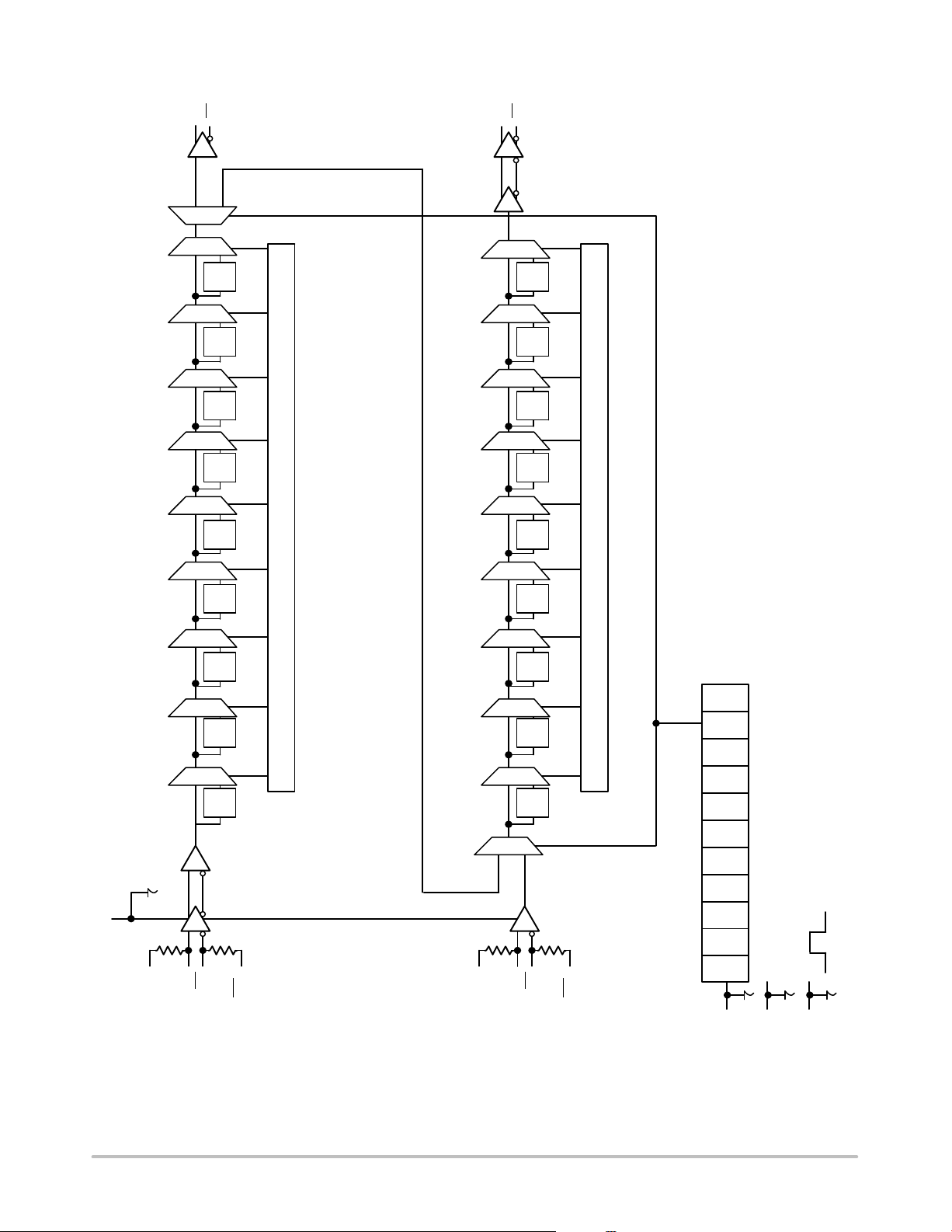
NB6L295M
Q0
Q0
0
1
0
1
1
GD*
0
1
2
GD*
0
1
4
GD*
0
1
8
GD*
Q1
0
0
0
0
Q1
1
1
GD*
1
2
GD*
1
4
GD*
1
8
GD*
PD0
0
0
1
16
GD*
0
1
32
GD*
0
1
64
GD*
0
1
128
GD*
0
1
256
GD*
9 Bit Latch
*GD = Gate Delay
PD1
1
16
GD*
0
1
32
GD*
0
1
64
GD*
0
1
128
GD*
0
1
256
GD*
0
1
9 Bit Latch
*GD = Gate Delay
PSEL
MSEL
D0
D1
D2
D3
D4
11 Bit Shift Register
D5
D6
D7
VT0
D8
50 W
IN0
IN0
50 W
VT0
VT1
50 W
IN1
IN1
50 W
VT1
SCKL
SDATA
SLOAD
Figure 1. Simplified Functional Block Diagram
http://onsemi.com
2
Page 3
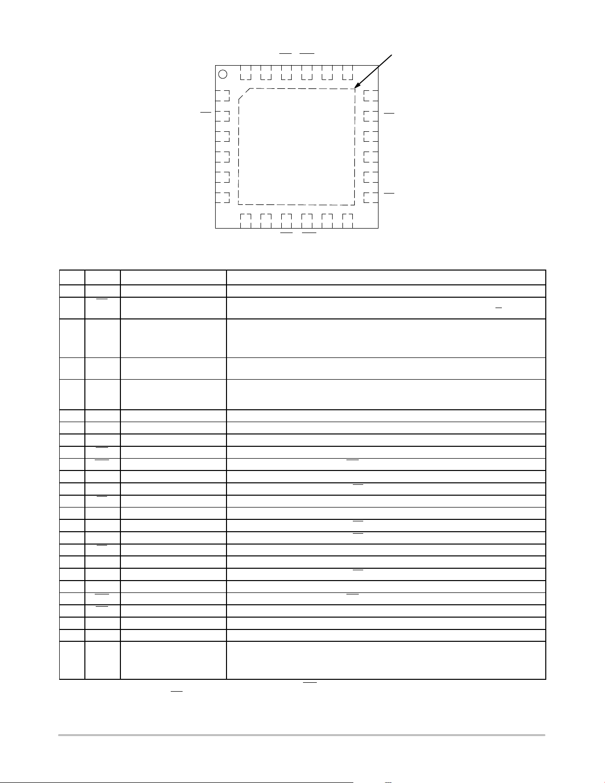
NB6L295M
Exposed Pad
(EP)
Q0
Q0
VCC0
VCC1
Q1
Q1
VCC
EN
SLOAD
SDIN
SCLK
VCC
VT0
1
2
3
4
5
6
789 1110
VT1
IN0
IN1
IN0
VT0
NB6L295M
IN1
GND
VCC0
1924 23 22 2021
18
17
16
15
14
13
12
VCC1GNDVT1
Figure 2. Pinout: QFN−24 (Top View)
Table 1. PIN DESCRIPTION
Pin Name I/O Description
1 VCC Power Supply Positive Supply Voltage for the Inputs and Core Logic
2 EN LVCMOS/LVTTL Input Input Enable/ Disable for both PD0 and PD1. LOW for enable, HIGH for disable, Open
3 SLOAD LVCMOS/LVTTL Input Serial Load; This pin loads the configuration latches with the contents of the shift
4 SDIN LVCMOS/LVTTL Input Serial Data In; This pin acts as the data input to the serial configuration shift register.
5 SCLK LVCMOS/LVTTL Input Serial Clock In; This pin serves to clock the serial configuration shift register. Data from
6 VCC Power Supply Positive Supply Voltage for the Inputs and Core Logic
7 VT1
8 IN1 LVPECL, CML, LVDS Input Noninverted differential input. Note 1. Channel 1.
9 IN1 LVPECL, CML, LVDS Input Inverted differential input. Note 1. Channel 1.
10 VT1
11 GND Power Supply Negative Power Supply
12 VCC1 Power Supply Positive Supply Voltage for the Q1/Q1 outputs, channel PD1
13 Q1 CML Output
14 Q1 CML Output
15 VCC1 Power Supply Positive Supply Voltage for the Q1/Q1 outputs, channel PD1
16 VCC0 Power Supply Positive Supply Voltage for the Q0/Q0 outputs, channel PD0
17 Q0 CML Output
18 Q0 CML Output
19 VCC0 Power Supply Positive Supply Voltage for the Q0/Q0 outputs, channel PD0
20 GND Power Supply Negative Power Supply
21 VT0
22 IN0 LVPECL, CML, LVDS Input Inverted differential input. Note 1. Channel 0.
23 IN0 LVPECL, CML, LVDS Input Noninverted differential input. Note 1. Channel 0.
24 VT0
− EP Ground The Exposed Pad (EP) on the QFN−24 package bottom is thermally connected to the
1. In the differential configuration when the input termination pin (VTx/VTx) are connected to a common termination voltage or left open, and
if no signal is applied on INx/INx
2. All VCC, VCC0 and VCC1 Pins must be externally connected to the same power supply for proper operation. Both VCC0s are connected
to each other and both VCC1s are connected to each other: VCC0 and VCC1 are separate.
input then the device will be susceptible to self−oscillation.
Pin Default state LOW (37 kW Pulldown Resistor). High Forces Q LOW and Q
register. The latches will be transparent when this signal is HIGH; thus, the data must be
stable on the HIGH−to−LOW transition of S_LOAD for proper operation. Open Pin
Default state LOW (37 kW Pulldown Resistor).
Open Pin Default state LOW (37 kW Pulldown Resistor).
SDIN is sampled on the rising edge. Open Pin Default state LOW (37 kW Pulldown
Resistor).
Internal 50 W Termination Pin for IN1.
Internal 50 W Termination Pin for IN1
Inverted Differential Output. Channel 1. Typically terminated with 50 W resistor to V
Noninverted Differential Output. Channel 1. Typically terminated with 50 W resistor to V
Inverted Differential Output. Channel 0. Typically terminated with 50 W resistor to V
Noninverted Differential Output. Channel 0. Typically terminated with 50 W resistor to V
Internal 50 W Termination Pin for IN0
Internal 50 W Termination Pin for IN0
die for improved heat transfer out of package. The exposed pad must be attached to a
heat−sinking conduit. The pad is electrically connected to GND and must be connected
to GND on the PC board.
HIGH.
CC1
CC1
CC0
CC0
http://onsemi.com
3
Page 4
NB6L295M
Table 2. ATTRIBUTES
Characteristics Value
Input Default State Resistors
ESD Protection Human Body Model
Machine Model
Moisture Sensitivity (Note 3) QFN−24 Level 1
Flammability Rating Oxygen Index: 28 to 34 UL 94 V−0 @ 0.125 in
Transistor Count 3094
Meets or exceeds JEDEC Spec EIA/JESD78 IC Latchup Test
3. For additional information, see Application Note AND8003/D.
Table 3. MAXIMUM RATINGS
Symbol Parameter Condition 1 Condition 2 Rating Unit
VCC, V
V
CC1
V
IO
V
INPP
I
IN
I
OUT
T
A
T
stg
q
JA
q
JC
T
sol
Stresses exceeding Maximum Ratings may damage the device. Maximum Ratings are stress ratings only. Functional operation above the
Recommended Operating Conditions is not implied. Extended exposure to stresses above the Recommended Operating Conditions may affect
device reliability.
4. JEDEC standard multilayer board − 2S2P (2 signal, 2 power) with 8 filled thermal vias under exposed pad.
,
Positive Power Supply GND = 0 V 4.0 V
CC0
Positive Input/Output Voltage GND = 0 V −0.5vVIOvVCC+0.5 4.5 V
Differential Input Voltage |INx − INx| VCC − GND V
Input Current Through R
Output Current Through R
(50 W Resistor)
T
(50 W Resistor)
T
Operating Temperature Range −40 to +85 °C
Storage Temperature Range −65 to +150 °C
Thermal Resistance (Junction−to−Ambient) (Note 4) 0 lfpm
500 lfpm
Thermal Resistance (Junction−to−Case) (Note 4) QFN−24 11 °C/W
Wave Solder Pb−Free 265 °C
QFN−24
QFN−24
37 kW
> 2 kV
> 100V
$50 mA
$50 mA
37
32
°C/W
°C/W
http://onsemi.com
4
Page 5
NB6L295M
Table 4. DC CHARACTERISTICS, MULTI−LEVEL INPUTS V
CC
= V
CC0
= V
= 2.375 V to 3.6 V, GND = 0 V, TA = −40°C to
CC1
+85°C
Symbol
Characteristic Min Typ Max Unit
POWER SUPPLY CURRENT
I
CC
Power Supply Current (Inputs, VTX and Outputs Open) (Sum of ICC,
I
CC0
, and I
CC1
)
170 215 mA
CML OUTPUTS (Notes 5 and 6, Figure 22)
V
OH
V
OL
Output HIGH Voltage
Output LOW Voltage
V
= V
CC
VCC = V
VCC = V
V
= V
CC
CC0
CC0
CC0
CC0
= V
= V
= V
= V
CC1
CC1
CC1
CC1
= 3.3 V
= 2.5 V
= 3.3 V
= 2.5 V
VCC − 40
3260
2460
VCC − 500
2800
2000
VCC − 10
3290
2490
VCC − 400
2900
2100
V
CC
3300
2500
VCC − 300
3000
2200
mV
mV
DIFFERENTIAL INPUT DRIVEN SINGLE−ENDED (see Figures 11 and 12) (Note 7)
V
th
V
IH
V
IL
V
ISE
Input Threshold Reference Voltage Range 1050 VCC − 150 mV
Single−Ended Input HIGH Voltage Vth +150 V
CC
mV
Single−Ended Input LOW Voltage GND Vth − 150 mV
Single−Ended Input Voltage Amplitude (VIH − VIL) 300 VCC − GND mV
DIFFERENTIAL INPUTS DRIVEN DIFFERENTIALLY (see Figures 13 and 14) (Note 8)
V
V
V
V
I
I
IHD
ILD
ID
CMR
IH
IL
Differential Input HIGH Voltage 1200 V
CC
Differential Input LOW Voltage GND VCC − 150 mV
Differential Input Voltage Swing (INx, INx) (V
IHD
− V
) 150 VCC − GND mV
ILD
Input Common Mode Range (Differential Configuration) (Note 9) 950 VCC – 75 mV
Input HIGH Current INx/INX, (VTn/VTn Open) −150 150
Input LOW Current IN/INX, (VTn/VTn Open) −150 150
mV
mA
mA
SINGLE−ENDED LVCMOS/LVTTL CONTROL INPUTS
V
IH
V
IL
I
IH
I
IL
Single−Ended Input HIGH Voltage 2000 V
CC
Single−Ended Input LOW Voltage GND 800 mV
Input HIGH Current −150 150
Input LOW Current −150 150
mV
mA
mA
TERMINATION RESISTORS
R
R
TIN
TOUT
Internal Input Termination Resistor 40 50 60
Internal Output Termination Resistor 40 50 60
W
W
NOTE: Device will meet the specifications after thermal equilibrium has been established when mounted in a test socket or printed circuit
board with maintained transverse airflow greater than 500 lfpm. Electrical parameters are guaranteed only over the declared
operating temperature range. Functional operation of the device exceeding these conditions is not implied. Device specification limit
values are applied individually under normal operating conditions and not valid simultaneously.
5. CML outputs loaded with 50 W to V
6. Input and output parameters vary 1:1 with V
, VIH, V
7. V
th
single−ended mode.
8. V
IHD
9. V
CMR
the differential input signal.
and V
IL,
, V
VID and V
ILD,
(min) varies 1:1 with voltage on GND pin, V
parameters must be complied with simultaneously. Vth is applied to the complementary input when operating in
ISE
parameters must be complied with simultaneously.
CMR
for proper operation.
CC
CC
.
CMR
(max) varies 1:1 with VCC. The V
range is referenced to the most positive side of
CMR
http://onsemi.com
5
Page 6

NB6L295M
Table 5. AC CHARACTERISTICS V
Symbol
f
SCLK
V
OUTPP
Serial Clock Input Frequency, 50% Duty Cycle 20 MHz
Output Voltage Amplitude (@ V
Characteristic Min Typ Max Unit
CC
INPPmin
(Note 15) (See Figure 23)
f
DATA
t
Range
Maximum Data Rate (Note 14) 2.5 Gb/s
Programmable Delay Range (@ 50 MHz)
Dual Mode IN0/IN0
to Q0/Q0 or IN1/IN1 to Q1/Q1
Extended Mode IN0/IN0 to Q1/Q1
t
SKEW
L
in
t
s
t
h
t
pwmin
t
JITTER
Duty Cycle Skew (Note 11)
Within Device Skew − Dual Mode D[8:0] = 0
Linearity (Note 12) $15 $20 ps
Setup Time (@ 20 MHz) SDIN to SCLK
Hold Time SDIN to SCLK
Minimum Pulse Width SLOAD 1 ns
Random Clock Jitter RMS; SETMIN to SETMAX
(Note 13) f
Dual Mode IN0/IN0 to Q0/Q0 or IN1/IN1 to Q1/Q1
Extended Mode IN0/IN0 to Q1/Q1
Deterministic Jitter; SETMIN to SETMAX (Note 14) f
v 2.5 Gbps
ATA
Dual Mode IN0/IN0 to Q0/Q0 or IN1/IN1 to Q1/Q1
V
t
INPP
r,
Input Voltage Swing/Sensitivity
(Differential Configuration) (Note 15)
t
Output Rise/Fall Times (@ 50 MHz), (20% − 80%)
f
Qx, Qx
Symbol Characteristic
t
,
t
PLH
PHL
Propagation Delay (@ 50 MHz)
Dual Mode IN0/IN0
to Q0/Q0 or IN1/IN1 to Q1/Q1
D[8:0] = 0
D[8:0] = 1
= V
= V
CC0
) fin ≤ 1.5 GHz
SCLK to SLOAD
EN
SCLK to SLOAD
EN
to SLOAD
≤ 1.5 GHz
in
= 2.375 V to 3.6 V, GND = 0 V, TA = −40°C to +85°C (Note 10)
CC1
210 380 mV
0
0
5.7
11.2
0 1
55
D[8:0] = 1
to SDIN
0.5
1.5
0.5
1.0
67
0.3
1.0
0.6 ns
1.0
0.5
2
4
D
2
150 VCC − GND mV
85 100 150 ps
−405C +255C +855C
Min Typ Max Min Typ Max Min Typ Max
2.7
3.1
3.3
2.8
3.2
7.2
8.5
9.1
7.4
8.5
3.5
9.6
3.1
8.6
6.9
13.7
4
96
170
6
12
15
3.4
9.3
ns
ps
ns
ps
Unit
ns
3.8
10.7
Extended Mode IN0/IN0 to Q1/Q1
D[8:0] = 0
D[8:0] = 1
Dt
Step Delay
5.0
14
5.9
16.4
6.5
17.7
5.2
14.4
6.2
16.6
6.6
18.7
5.9
17
6.6
19
7.3
21
(Selected D Bit HIGH All Others LOW)
D0 HIGH
D1 HIGH
D2 HIGH
D3 HIGH
D4 HIGH
D5 HIGH
D6 HIGH
D7 HIGH
D8 HIGH
8.4
16.4
41.2
85
178
360
722
1448
2903
12.4
25.1
58.3
108
210
405
796
1579
3143
NOTE: Device will meet the specifications after thermal equilibrium has been established when mounted in a test socket or printed circuit
board with maintained transverse airflow greater than 500 lfpm. Electrical parameters are guaranteed only over the declared
operating temperature range. Functional operation of the device exceeding these conditions is not implied. Device specification limit
values are applied individually under normal operating conditions and not valid simultaneously.
10.Measured by forcing V
= 50 W to VCC. See Figure 20. Input edge rates 40 ps (20% − 80%).
R
L
11.Duty cycle skew is measured between differential outputs using the deviations of the sum of T
12.Deviation from a linear delay (actual Min to Max) in the Dual Mode 511 programmable steps; 3.3 V @ 25°C, 400 mV V
13.Additive Random CLOCK jitter with 50% duty cycle input clock signal. 1000 WFMS, JIT3 Software.
INPPmin
and V
from a 50% duty cycle clock source, V
INPPmax
(min and max). All loading with an external
CMR
− and Tpw+ @ 0.5 GHz.
pw
INPP
.
14.NRZ data at PRBS23 and K28.5. 10,000 WFMS, TDS8000.
15.Input and output voltage swing is a single−ended measurement operating in differential mode.
http://onsemi.com
6
ps
Page 7

NB6L295M
Serial Data Interface Programming
The NB6L295M is programmed by loading the 11−Bit SHIFT REGISTER using the SCLK, SDATA and SLOAD inputs.
The 11 SDATA bits are 1 PSEL bit, 1 MSEL bit and 9 delay value data bitsD[8:0]. A separate 11−bit load cycle is required to
program the delay data value of each channel, PD0 and PD1. For example, at powerup two load cycles will be needed to initially
set PD0 and PD1; Dual Mode Operation as shown in Figures 3 and 4 and Extended Mode Operation as shown in Figures 5
and 6.
DUAL MODE OPERATIONS
Control
PD0 Programmable Delay
0/1 0/1 0/1 0/1 0/1 0/1 0/1 0/1 0/1 0 0 0/1 0/1 0/1 0/1 0/1 0/1 0/1 0/1 0/1 0 1
D8 D7 D6 D5 D4 D3 D2 D1 D0 MSEL PSEL
(MSB) (LSB)
Bits
PD1 Programmable Delay
Value
Bit
Name
D8 D7 D6 D5 D4 D3 D2 D1 D0 MSEL PSEL
(MSB) (LSB)
Figure 3. PDO Shift Register Figure 4. PD1 Shift Register
EXTENDED MODE OPERATIONS
Control
PD0 Programmable Delay
0/1 0/1 0/1 0/1 0/1 0/1 0/1 0/1 0/1 1 0 0/1 0/1 0/1 0/1 0/1 0/1 0/1 0/1 0/1 1 1
D8 D7 D6 D5 D4 D3 D2 D1 D0 MSEL PSEL
(MSB) (LSB)
Bits
PD1 Programmable Delay
Value
Bit
Name
D8 D7 D6 D5 D4 D3 D2 D1 D0 MSEL PSEL
(MSB) (LSB)
Figure 5. PDO Shift Register Figure 6. PD1 Shift Register
Refer to Table 6, Channel and Mode Select BIT Functions. In a load cycle, the 11−Bit Shift Register least significant bit
(clocked in first) is PSEL and will determine which channel delay buffer, either PDO (LOW) or PD1 (HIGH), will latch the
delay data value D[8:0]. The MSEL BIT determines the Delay Mode. When set LOW, the Dual Delay Mode is selected and
the device uses both channels independently. A pulse edge entering IN0/IN0
from Q0/Q0
. An input signal pulse edge entering IN1/IN1 is delayed according to the values in PD1 and exits from Q1/Q1.
is delayed according to the values in PD0 and exits
When MSEL is set HIGH, the Extended Delay Mode is selected and an input signal pulse edge enters IN0 and IN0
through PD0 and is extended through PD1 to exit at Q1 and Q1
. The most significant 9−bits, D[8:0] are delay value data for
both channels. See Figure 7.
Control
Bits
Value
Bit
Name
Control
Bits
Value
Bit
Name
and flows
Table 6. CHANNEL AND MODE SELECT BIT FUNCTIONS
BIT Name Function
PSEL
MSEL
D[8:0] Select one of 512 Delay Values
0 Loads Data to PD0
1 Loads Data to PD1
0 Selects Dual Programmable Delay Paths, 3.1 ns to 8.8 ns Delay Range for Each Path
1 Selects Extended Delay Path from IN0/IN0 to Q1/Q1, 6.0 ns to 17.2 ns Delay Range; Disables Q0/Q0 Outputs,
Q0−LOW, Q0
−HIGH.
http://onsemi.com
7
Page 8

NB6L295M
SLOAD
Q0/Q0
PD0 Delay PD1 Delay
MSEL
D8D7D6D5D4D3D2D1D0
01
SDATA
SCLK
D8D7D6D5D4D3D2D1D0
11−Bit Shift Register
D8D7D6D5D4D3D2D1D0
MSEL
PSEL
PD1 LatchPD0 Latch
Q1/Q1
Figure 7. Serial Data Interface, Shift Register, Data Latch, Programmable Delay Channels
Load Cycle Required for Each Channel
Serial Data Interface Loading
Loading the device through the 3 input Serial Data Interface (SDI) is accomplished by sending data into the SDIN pin by
using the SCLK input pin and latching the data with the SLOAD input pin. The 11−bit SHIFT REGISTER shifts once per rising
edge of the SCLK input. The serial input SDIN must meet setup and hold timing as specified in the AC Characteristics section
of this document for each bit and clock pulse. The SLOAD line loads the value of the shift register on a LOW−to−HIGH edge
transition (transparent state) into a data Latch register and latches the data with a subsequent HIGH−to−LOW edge transition.
Further changes in SDIN or SCLK are not recognized by the latched register. The internal multiplexer states are set by the PSEL
and MSEL bits in the SHIFT register. Figure 6 shows the timing diagram of a typical load sequence.
Input EN
programming, the EN
The disabling of EN
should be LOW (enabled) prior to SDI programming, then pulled HIGH (disabled) during programming. After
should be returned LOW (enabled) for functional delay operation.
(HIGH) forces Qx LOW and Qx HIGH and is included during programming to prevent (or mask out)
any potential run pulses or extended pulses which might occur in the internal delay gates programming switching, but it is not
required for programming.
EN
SDIN
SCLK
EN to SDIN
LSB
PSEL MSEL D0 D1 D2 D3 D5 D6
C0 C1 C2 C3 C4 C5 C6 C7 C8 C9 C10
D4 D8D7
MSB
EN
to SLOAD
SLOAD
ts SDIN to
SCLK
t
SCLK to SLOAD
s
t
SDIN to SCLK
h
Figure 8. SDI Programming Cycle Timing Diagram (Load Cycle 1 of 2)
http://onsemi.com
8
SCLK to SLOAD
t
H
Page 9

NB6L295M
Table 7 shows theoretical values of delay capabilities in both the Dual Delay Mode and in the Extended Delay Modes of
operation.
Table 7. EXAMPLES OF THEORETICAL DELAY VALUES FOR PD0 AND PD1 IN DUAL MODE
INPUTS: IN0/IN0, IN1/IN1, OUTPUTS: Q0/Q0, Q1, Q1
Dual Mode
PD1 D[8:0] (Decimal) PD0 D[8:0] (Decimal) MSEL
000000000 (0) 000000000 (0) 0 0 0
000000000 (0) 000000001 (1) 0 11 0
000000000 (0) 000000010 (2) 0 22 0
000000000 (0) 000000011 (3) 0 33 0
000000000 (0) 000000100 (4) 0 44 0
000000000 (0) 000000101 (5) 0 55 0
000000000 (0) 000000110 (6) 0 66 0
000000000 (0) 000000111 (7) 0 77 0
000000000 (0) 000001000 (8) 0 88 0
•
•
•
000000000 (0) 000010000 (16) 0 176 0
000000000 (0) 000100000 (32) 0 352 0
000000000 (0) 001000000 (64) 0 704 0
000000000 (0) 11111110 1 (509) 0 5599 0
000000000 (0) 111111110 (510) 0 5610 0
000000000 (0) 111111111 (511) 0 5621 0
*Fixed minimum delay not included
Table 8. EXAMPLES OF THEORETICAL DELAY VALUES FOR PD0 AND PD1 IN EXTENDED MODE
INPUTS: IN0/IN0, IN1/IN1, OUTPUTS: Q0/Q0, Q1, Q1
Extended Delay Mode
PD1 D[8:0]
000000000 (0) 000000000 (0) 1 0 0 0
000000000 (0) 000000001 (1) 1 0 11 11
000000000 (0) 000000010 (2) 1 0 22 22
000000000 (0) 000000011 (3) 1 0 33 33
000000000 (0) 111111101 (509) 1 0 5599 5599
000000000 (0) 11111111 0 (510) 1 0 5610 5610
000000000 (0) 111111111 (511) 1 0 5621 5621
000000001 (1) 111111111 (511) 1 11 5621 5632
000000010 (2) 111111111 (511) 1 22 5621 5643
11111110 0 (508) 111111111 (511) 1 5588 5621 11209
11111110 1 (509) 111111111 (511) 1 5599 5621 11220
111111110 (510) 111111111 (511) 1 5610 5621 11231
111111111 (511) 111111111 (511) 1 5621 5621 11242
*Fixed minimum delay not included
(Decimal)
PD0 D[8:0]
•
•
•
•
•
•
(Decimal)
MSEL
PD0 Delay* (ps) PD1 Delay* (ps)
•
•
•
PD0* (ps) PD1* (ps) Total Delay* (ps)
•
•
•
•
•
•
•
•
•
•
•
•
•
•
•
•
•
•
•
•
•
http://onsemi.com
9
Page 10

NB6L295M
VTx
V
50 W
INx
INx
50 W
VTx
Figure 9. Input Structure
V
IH
V
th
V
IL
INx
V
th
Figure 11. Differential Input Driven
Single−Ended
CC
I
INx
V
CCO
50 W 50 W
50 W 50 W
16 mA
GND
Figure 10. Typical CML Output Structure
and Termination
V
CC
V
thmax
V
th
V
thmin
GND
Figure 12. Vth Diagram
VCC (Receiver)
V
IHmax
V
ILmax
V
IH
V
th
V
IL
V
IHmin
V
ILmin
V
CC
V
GND
INx
INx
Figure 13. Differential Inputs
Driven Differentially
CMR
Figure 15. V
Diagram Figure 16. AC Reference Measurement
CMR
V
IHD(MAX)
V
ILD(MAX)
V
IHD
VID = V
V
ILD
V
IHD(MIN)
V
ILD(MIN)
IHD
− V
ILD
http://onsemi.com
10
INx
INx
Qx
Qx
INx
INx
VID = |V
V
IHD
V
ILD
IHD(INx)
− V
ILD(INx)|
Figure 14. Differential Inputs Driven
Differentially
V
= VIH(INx) − VIL(INx)
INPP
V
= VOH(Qx) − VOL(Qx)
OUTPP
t
PD
t
PD
Page 11

NB6L295M
V
CC
Zo = 50 W
LVPECL
Driver
VTx
VTx
Zo = 50 W
VTx = VTx = VCC − 2.0 V
GND
Figure 17. LVPECL Interface
INx
INx
V
CC
NB6L295M
50 W
50 W
GND
V
CC
CML
Driver
Zo = 50 W
VTx
V
CC
VTx
INx
V
CC
LVDS
Driver
V
CC
NB6L295M
50 W*
50 W*
INx
Zo = 50 W
VTx
VTx
Zo = 50 W
V
T
x = VTx
INx
Figure 18. LVDS Interface
V
CC
NB6L295M
50 W*
50 W*
GNDGND
V
CC
Differential
Driver
GND
Zo = 50 W
V
REFAC
Zo = 50 W
V
x = VTx = External V
T
VTx
VTx
Zo = 50 W
INx
V
x = VTx = V
T
CC
GND
Figure 19. CML Interface, Standard 50 W Load
V
CC
INx
NB6L295M
50 W*
50 W*
INx
REFAC
GND
GND
V
CC
Single−Ended
Driver
V
GND
Zo = 50 W
VTx
V
REFAC
VTx
x = VTx = External V
T
INx
INx
REFAC
V
CC
NB6L295M
50 W*
50 W*
GND
Figure 20. Capacitor−Coupled Differential
Interface (V
V
REFAC
x/VTx Connected to V
T
REFAC
Bypassed to Ground with 0.1 mF
Capacitor)
;
http://onsemi.com
11
Figure 21. Capacitor−Coupled Single−Ended
Interface (V
V
REFAC
x/VTx Connected to External V
T
Bypassed to Ground with 0.1 mF Capacitor)
REFAC
;
Page 12

NB6L295M
V
CC
50 W50 W
Receiver
Device
DUT
Driver
Device
Z = 50 W
QD
Z = 50 W
Q D
Figure 22. Typical Termination for Output Driver and Device Evaluation
800
700
600
500
400
300
AMPLITUDE (mV)
200
, TYPICAL OUTPUT VOLTAGE
100
OUTPP
V
0
1.51.00.50
f
, CLOCK OUTPUT FREQUENCY (GHz)
OUT
Figure 23. Output Voltage Amplitude (V
OUTPP
) vs.
Output Frequency at Ambient Temperature (Typical)
ORDERING INFORMATION
Device Package Shipping
NB6L295MMNG QFN−24
(Pb−free)
NB6L295MMNTXG QFN−24
(Pb−free)
†For information on tape and reel specifications, including part orientation and tape sizes, please refer to our Tape and Reel Packaging
Specifications Brochure, BRD8011/D.
92 Units / Rail
3000 / Tape & Reel
†
http://onsemi.com
12
Page 13

MECHANICAL CASE OUTLINE
PACKAGE DIMENSIONS
24
1
SCALE 2:1
D
PIN 1
REFEENCE
2X
0.15 C
2X
0.15 C
TOP VIEW
DETAIL B
0.10 C
0.08 C
NOTE 4
DETAIL A
1
SIDE VIEW
D2
7
24
e
e/2
BOTTOM VIEW
RECOMMENDED
SOLDERING FOOTPRINT
4.30
2.90
1
A3
A
B
E
A
SEATING
24X
C
PLANE
L
A1
13
E2
19
b
24X
0.10 B
0.05
0.55
24X
C
AC
NOTE 3
QFN24, 4x4, 0.5P
CASE 485L
ISSUE B
L1
DETAIL A
ALTERNATE
CONSTRUCTIONS
MOLD CMPDEXPOSED Cu
DETAIL B
ALTERNATE TERMINAL
CONSTRUCTIONS
DATE 05 JUN 2012
A3
NOTES:
1. DIMENSIONING AND TOLERANCING PER ASME
Y14.5M, 1994.
2. CONTROLLING DIMENSION: MILLIMETERS.
3. DIMENSION b APPLIES TO PLATED TERMINAL
AND IS MEASURED BETWEEN 0.25 AND 0.30 MM
FROM THE TERMINAL TIP.
4. COPLANARITY APPLIES TO THE EXPOSED PAD
AS WELL AS THE TERMINALS.
MILLIMETERS
DIM MIN MAX
A 0.80 1.00
A1 0.00 0.05
A3 0.20 REF
b 0.20 0.30
D 4.00 BSC
D2 2.70 2.90
E 4.00 BSC
E2 2.70 2.90
e 0.50 BSC
L 0.30 0.50
L1 0.05 0.15
L
L
A1
GENERIC
MARKING DIAGRAM*
XXXXX
XXXXX
ALYWG
G
XXXXX = Specific Device Code
A = Assembly Location
L = Wafer Lot
Y = Year
W = Work Week
G = Pb−Free Package
(Note: Microdot may be in either location)
*This information is generic. Please refer to
device data sheet for actual part marking.
Pb−Free indicator, “G” or microdot “ G”,
may or may not be present.
24X
0.32
4.30
Electronic versions are uncontrolled except when accessed directly from the Document Repository.
Printed versions are uncontrolled except when stamped “CONTROLLED COPY” in red.
PAGE 1 OF 1
www.onsemi.com
2.90
0.50
PITCH
DOCUMENT NUMBER:
DESCRIPTION:
ON Semiconductor and are trademarks of Semiconductor Components Industries, LLC dba ON Semiconductor or its subsidiaries in the United States and/or other countries.
ON Semiconductor reserves the right to make changes without further notice to any products herein. ON Semiconductor makes no warranty, representation or guarantee regarding
the suitability of its products for any particular purpose, nor does ON Semiconductor assume any liability arising out of the application or use of any product or circuit, and specifically
disclaims any and all liability, including without limitation special, consequential or incidental damages. ON Semiconductor does not convey any license under its patent rights nor the
rights of others.
© Semiconductor Components Industries, LLC, 2019
DIMENSIONS: MILLIMETERS
98AON11783D
QFN24, 4X4, 0.5P
Page 14

ON Semiconductor and are trademarks of Semiconductor Components Industries, LLC dba ON Semiconductor or its subsidiaries in the United States and/or other countries.
ON Semiconductor owns the rights to a number of patents, trademarks, copyrights, trade secrets, and other intellectual property. A listing of ON Semiconductor ’s product/patent
coverage may be accessed at www.onsemi.com/site/pdf/Patent−Marking.pdf
ON Semiconductor makes no warranty, representation or guarantee regarding the suitability of its products for any particular purpose, nor does ON Semiconductor assume any liability
arising out of the application or use of any product or circuit, and specifically disclaims any and all liability, including without limitation special, consequential or incidental damages.
Buyer is responsible for its products and applications using ON Semiconductor products, including compliance with all laws, regulations and safety requirements or standards,
regardless of any support or applications information provided by ON Semiconductor. “Typical” parameters which may be provided in ON Semiconductor data sheets and/or
specifications can and do vary in different applications and actual performance may vary over time. All operating parameters, including “Typicals” must be validated for each customer
application by customer’s technical experts. ON Semiconductor does not convey any license under its patent rights nor the rights of others. ON Semiconductor products are not
designed, intended, or authorized for use as a critical component in life support systems or any FDA Class 3 medical devices or medical devices with a same or similar classification
in a foreign jurisdiction or any devices intended for implantation in the human body. Should Buyer purchase or use ON Semiconductor products for any such unintended or unauthorized
application, Buyer shall indemnify and hold ON Semiconductor and its officers, employees, subsidiaries, affiliates, and distributors harmless against all claims, costs, damages, and
expenses, and reasonable attorney fees arising out of, directly or indirectly, any claim of personal injury or death associated with such unintended or unauthorized use, even if such
claim alleges that ON Semiconductor was negligent regarding the design or manufacture of the part. ON Semiconductor is an Equal Opportunity/Affirmative Action Employer. This
literature is subject to all applicable copyright laws and is not for resale in any manner.
. ON Semiconductor reserves the right to make changes without further notice to any products herein.
PUBLICATION ORDERING INFORMATION
LITERATURE FULFILLMENT:
Email Requests to: orderlit@onsemi.com
ON Semiconductor Website: www.onsemi.com
TECHNICAL SUPPORT
North American Technical Support:
Voice Mail: 1 800−282−9855 Toll Free USA/Canada
Phone: 011 421 33 790 2910
Europe, Middle East and Africa Technical Support:
Phone: 00421 33 790 2910
For additional information, please contact your local Sales Representative
◊
www.onsemi.com
1
 Loading...