

Page 1
NB4N441
3.3V Serial Input
MultiProtocol PLL Clock
Synthesizer, Differential
LVPECL Output
Description
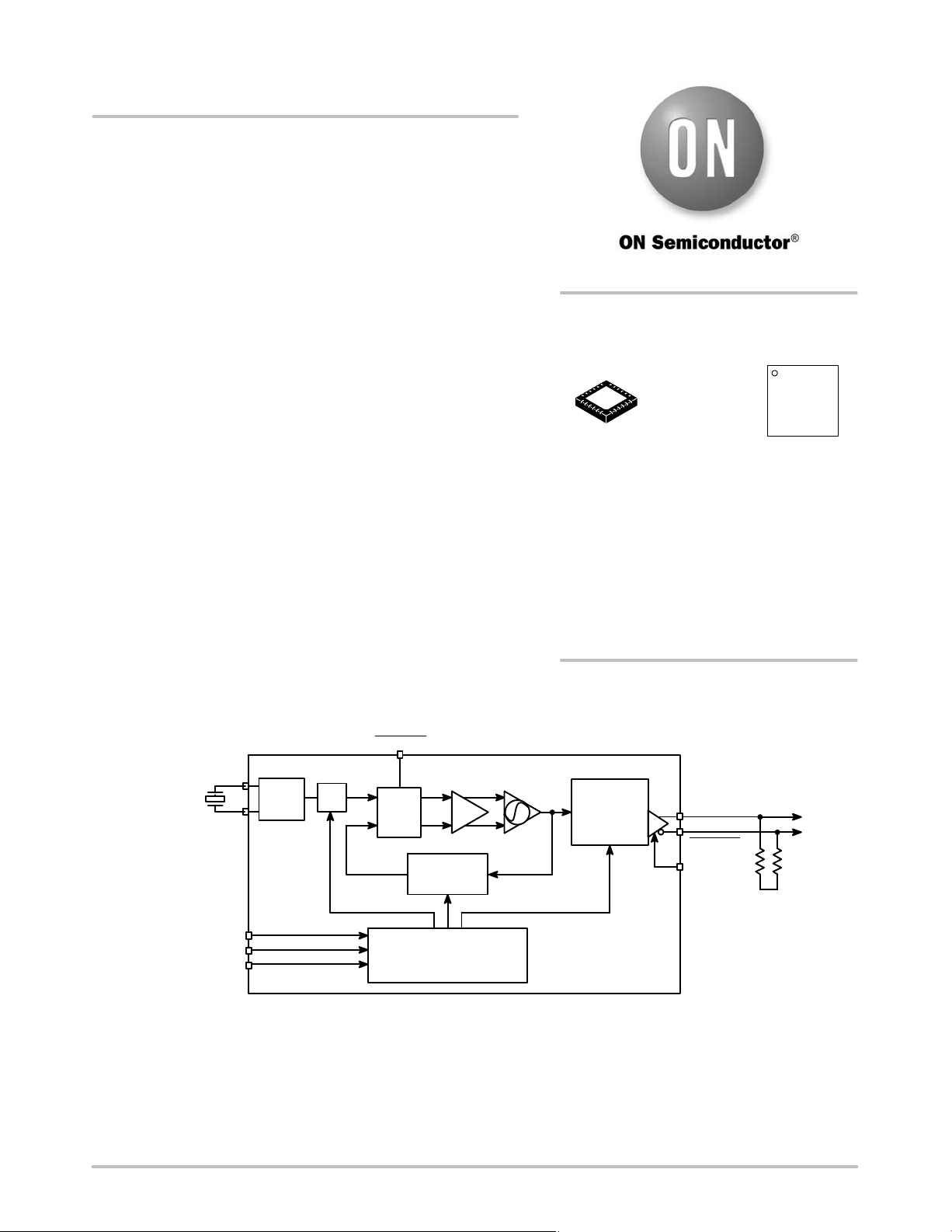
The NB4N441 is a precision clock synthesizer which generates a
differential LVPECL clock output frequency from 12.5 MHz to
425 MHz. A Serial Peripheral Interface (SPI) is used to configure the
device to produce one of sixteen popular standard protocol output
frequencies from a single 27 MHz crystal reference. The NB4N441
also has the added feature of allowing application specific output
frequencies from 12.5 MHz to 425 MHz using crystals within the
range of 10 MHz to 28 MHz.
http://onsemi.com
1
QFN−24
MN SUFFIX
CASE 485L
MARKING
DIAGRAM*
24
NB4N
441
ALYWG
G
Features
• Performs Precision Clock Generation and Synthesis from a Single
27 MHz Crystal Reference
• Serial Load Capability for Proprietary Frequencies
• Flexible Input Allows for External Clock Reference
• Exceeds Bellcore and ITU Jitter Generation Specification
• PLL Lock Detect Output
• Output Enable
• Fully Integrated Phase−Lock−Loop with Internal Loop Filter
• Operating Range: V
= 3.135 V to 3.465 V
CC
• Small Footprint 24 Pin QFN
• These are Pb−Free Devices*
LOCKED
27 MHz
XTAL
OSC
B
R
FB
Feedback
Divider
A = Assembly Location
L = Wafer Lot
Y = Year
W = Work Week
G = Pb−Free Package
(Note: Microdot may be in either location)
*For additional marking information, refer to
Application Note AND8002/D.
ORDERING INFORMATION
See detailed ordering and shipping information in the package
dimensions section on page 11 of this data sheet.
OUTDIV
B2, 4, 8,
16, 32
CLKOUT
CLKOUT
OE
VCC − 2 V
SDATA
SCLOCK
SLOAD
*For additional information on our Pb−Free strategy and soldering details, please
download the ON Semiconductor Soldering and Mounting Techniques
Reference Manual, SOLDERRM/D.
© Semiconductor Components Industries, LLC, 2011
April, 2011 − Rev. 2
Frequency Control Logic
Serial Load
Figure 1. Simplified Block Diagram
1 Publication Order Number:
NB4N441/D
Page 2
NB4N441
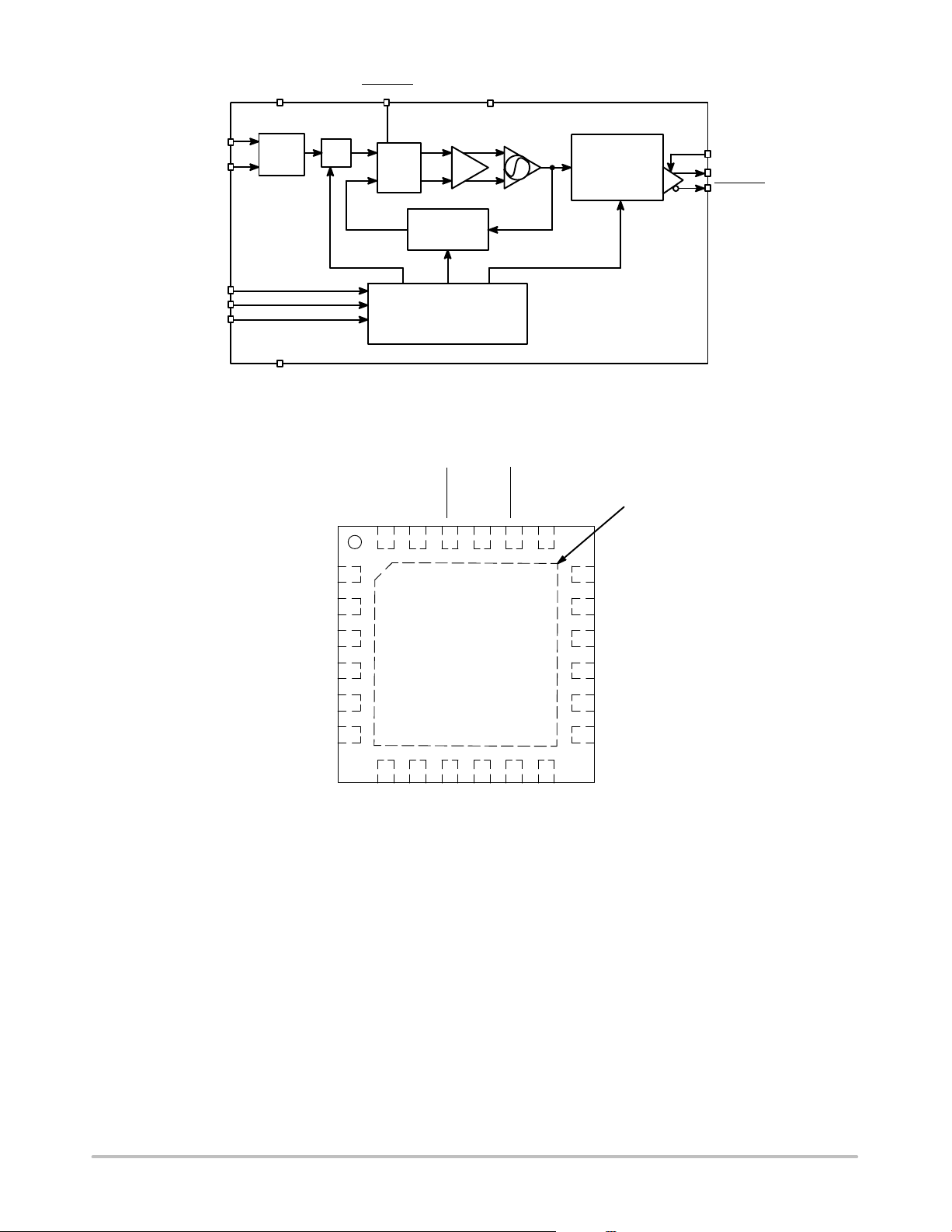
CLK/XTAL1
XTAL2
SDATA
SCLOCK
SLOAD
V
CC
XTAL
OSC
GND
Input
Prescaler
PB
LOCKED
PFD
VCC_PLL
Loop
Filter
R
FB
Feedback
Divider (MB)
P[4:0] M[9:0] N[3:0]
Frequency Control Logic
Serial Load
Figure 2. Block Diagram
CC
V
CLKOUT
CLKOUT
OE
VCO
LOCKED
GND
1924 23 22 2021
OUTDIV (NB)
B2, 4, 8,
16, 32
Exposed Pad
(EP)
OE
CLKOUT
CLKOUT
GND
NC
VCC_PLL
NC
NC
GND
1
2
3
4
5
6
789 1110
XTAL2
GND
NC
CC
V
18
17
16
15
14
13
12
CC
V
CLK/XTAL1
Figure 3. QFN−24 Lead Pinout (Top View)
GND
SCLOCK
SDATA
SLOAD
NC
V
CC
http://onsemi.com
2
Page 3
NB4N441
Table 1. PIN DESCRIPTION
Pin Name I/O Description
11, 12, 13, 24 V
3 VCC_PLL PLL Power Supply Positive supply voltage for the PLL.
1, 6, 9, 18, 19 GND Ground Ground.
20 LOCKED LVTTL Lock Output When Low, this output provides indication that the PLL is
2, 4, 5, 10, 14 NC No Connect.
8 CLK / XTAL1,
7 XTAL2
15 SLOAD** LVTTL / LVCMOS,
16 SDATA** LVTTL / LVCMOS
17 SCLOCK** LVTTL / LVCMOS
21 OE* LVTTL Input Synchronous Output Enable. When OE is HIGH or left
22, 23 CLKOUT
*Pins will default HIGH when left Open
**Pins will default LOW when left Open
CC
CLKOUT
EP The Exposed Pad on the 24 pin QFN package bottom is
Power Supply Positive supply voltage.
locked and the device is in proper operating mode. When
High, the PLL is out of lock.
LVTTL/LVCMOS Single Ended
Clock or XTAL Inputs
Serial Load Input
Serial Data Input
Serial Clock Input
LVPECL Output Differential LVPECL Clock Outputs, Typically terminated with
The crystal is connected between the XTAL1 and XTAL2 pin.
If driving single−ended, use XTAL1 and leave XTAL2
floating.
Serial Load.
Serial Data Input.
Serial Clock Input.
OPEN, the outputs are enabled. When OE is LOW, the
outputs are disabled.
50 W resistor to VCC – 2.0 V.
thermally connected to the die for improved heat transfer out
of package. The pad is not electrically connected to the die,
but is recommended to be electrically connected to GND on
the PC board.
http://onsemi.com
3
Page 4
NB4N441
Table 2. STANDARD PROTOCOL / OUTPUT FREQUENCY SELECT TABLE WITH 27 MHz CRYSTAL REFERENCE
Input Prescaler
# Protocol CLKOUT (MHz)
0 OC−3 /STM−1 155.52 11001 1001000000 010
0 OC−12 / STM−4 155.52 11001 1001000000 010
0 OC−48 / STM−16 155.52 11001 1001000000 010
1 ETR 32 11011 1000000000 100
2 OC−1 51.84 11001 1100000000 100
3 Fast Ethernet 50 11011 1100100000 100
3 ESCON 50 11011 1100100000 100
4 FDDI 125 11011 0111110100 010
4 Infiniband 125 11011 0111110100 010
4 Gigabit Ethernet 125 11011 0111110100 010
4 PCIe 125 11011 0111110100 010
5 1/8 Fibre Channel 13.28125 11011 0110101001 101
6 1/4 Fibre Channel 26.5625 11011 1101010010 101
7 1/2 Fibre Channel 53.125 11011 1101010010 100
8 Fibre Channel 106.25 11011 1101010010 011
9 General 150 11011 1001011000 010
10 D1 Video 69 11011 1000101000 011
11 SONET Reference 19.44 11001 1001000000 101
12 2x Fibre Channel 212.5 11011 1101010010 010
13 4x Fibre Channel 425 11011 1101010010 001
14 XAUI 156.25 11011 1001110001 010
15 Serial ATA 100 11011 1100100000 011
16 HDTV 74.25 11011 1001010010 011
17 HDTV 148.50 11011 1001010010 010
Divider P[4:0]
PLL FB Divider
M[9:0]
Output Frequency Divider
OUTDIV N[2:0]
Table 3. N−DIVIDER TABLE
N2 N1 N0 N Divider
0 0 0 na
0 0 1 B2
0 1 0 B4
0 1 1 B8
1 0 0 B16
1 0 1 B32
1 1 0 na
1 1 1 na
http://onsemi.com
4
Page 5

NB4N441
Table 4. ATTRIBUTES
Characteristics Value
Internal Input Pullup Resistor
Internal Input Pulldown Resistor
ESD Protection Human Body Model
Machine Model
Moisture Sensitivity (Note 1) Level 1
Flammability Rating Oxygen Index: 28 to 34 UL 94 V−0 @ 0.125 in
Transistor Count 2102
Meets or exceeds JEDEC Spec EIA/JESD78 IC Latchup Test
1. For additional information, see Application Note AND8003/D.
Table 5. MAXIMUM RATINGS (Note 2)
Symbol
V
CC
V
I
I
out
T
A
T
stg
q
JA
q
JC
T
sol
Positive Power Supply GND = 0 V 3.6 V
Input Voltage GND = 0 V GND = VI = V
LVPECL Output Current Continuous Surge 50
Operating Temperature Range QFN−24 −40 to +85 °C
Storage Temperature Range −65 to +150 °C
Thermal Resistance (Junction−to−Ambient) (Note 3) 0 lfpm
Thermal Resistance (Junction−to−Case) 2S2P (Note 3) QFN−24 °C/W
Wave Solder < 3 sec @ 260°C 265 °C
Stresses exceeding Maximum Ratings may damage the device. Maximum Ratings are stress ratings only. Functional operation above the
Recommended Operating Conditions is not implied. Extended exposure to stresses above the Recommended Operating Conditions may affect
device reliability.
2. Maximum Ratings are those values beyond which device damage may occur.
3. JEDEC standard multilayer board − 2S2P (2 signal, 2 power).
Parameter Condition 1 Condition 2 Rating Unit
500 lfpm
37.5kW
75kW
> 1000 V
> 150 V
QFN−24
QFN−24
CC
3.6 V
100
°C/W
°C/W
mA
mA
http://onsemi.com
5
Page 6

NB4N441
Table 6. DC CHARACTERISTICS V
Symbol
I
CC
I
CCPLL
V
OH
V
OL
V
OHTTL
V
OLTTL
V
IH
V
IL
I
IH
I
IL
Power Supply Current (Inputs and Outputs Loaded) 50 70 90 mA
PLL Power Supply Current 10 20 30 mA
LVPECL Output HIGH Voltage (Notes 4 and 5)
LVPECL Output LOW Voltage (Notes 4 and 5)
Output HIGH Voltage (LOCKED Pin) IOH = −0.8 mA 2.5 V
Output LOW Voltage (LOCKED Pin) GND 0.4 V
Input HIGH Voltage (LVTTL/LVCMOS) 2.0 V
Input LOW Voltage (LVTTL/LVCMOS) GND 0.8 V
Input HIGH Current, OE VIN = 2.7 V, VCC
SCLK, SDATA, SLOAD VIN = 2.7 V, VCC
OE, SCLK, SDATA, SLOAD VIN = VCC, VCC
Input LOW Current VIN = 0.5 V, VCC
= 3.135 V to 3.465 V, GND = 0 V, TA = −40°C to +85°C
CC
Characteristic Min Typ Max Unit
V
V
= 3.3 V
CC
= 3.3 V
CC
max
max
max
max
VCC – 1145
2155
VCC – 1945
1355
6.0
20
20
VCC − 1030
2270
VCC − 1760
1540
VCC – 895
2405
VCC – 1695
1605
CC
CC
26
60
60
10
NOTE: Device will meet the specifications after thermal equilibrium has been established when mounted in a test socket or printed circuit
board with maintained transverse airflow greater than 500 lfpm. Electrical parameters are guaranteed only over the declared
operating temperature range. Functional operation of the device exceeding these conditions is not implied. Device specification limit
values are applied individually under normal operating conditions and not valid simultaneously.
4. LVPECL Outputs loaded with 50 W termination resistors to V
5. LVPECL Output parameters vary 1:1 with V
CC
.
= VCC – 2.0 V for proper operation.
TT
mV
mV
V
V
mA
mA
mA
Table 7. AC CHARACTERISTICS V
Symbol
f
IN
V
OUTPP
f
VCO
f
CLKOUT
tR/t
F_IN
t
LOCK
Crystal Input Frequency
External CLOCK Input Frequency (Pin 8)
SCLOCK
Output Voltage Amplitude 600 800 mV
VCO Frequency Range 400 850 MHz
Output Clock Frequency Range 12.5 425 MHz
Input Clock Rise and Fall Time (CLK, Pin 8) (Note 7) 10 ns
Maximum PLL Lock Time 0.5 5 ms
= 3.135 V to 3.465 V, GND = 0 V, TA = −40°C to +85°C (Note 6)
CC
Characteristic Min Typ Max Unit
10 27
27
28
50
MHz
10
DCO Output CLOCK Duty Cycle (Differential Configuration) 48 52 %
t
JITTER(pd)
t
JITTER(pd)
t
s
t
h
t
pwmin
tr, t
f
Period Jitter (RMS, 1s, 10,000 Cycles) (Notes 8 and 9)
Period Jitter (Peak−to−Peak, 10,000 Cycles) (Note 9) 25 40 ps
Setup Time SDATA to SCLOCK
SCLOCK to SLOAD
Hold Time SDATA to SCLOCK
SCLOCK to SLOAD
20
20
20
20
Minimum Pulse Width SLOAD 20 ns
Output Rise/Fall Times (Note 7) CLKOUT / CLKOUT 175 300 425 ps
3.5 6.5 ps
NOTE: Device will meet the specifications after thermal equilibrium has been established when mounted in a test socket or printed circuit
board with maintained transverse airflow greater than 500 lfpm. Electrical parameters are guaranteed only over the declared
operating temperature range. Functional operation of the device exceeding these conditions is not implied. Device specification limit
values are applied individually under normal operating conditions and not valid simultaneously.
6. LVPECL Outputs loaded with 50 W to V
7. Measured 20% to 80%
8. Additive RMS jitter with 50% duty cycle input clock signal at 27.000 MHz; f
= 155 MHz. Protocol 13.28125 MHz will have typical period jitter (RMS) of 14 ps and a typical cycle−to−cycle jitter of 95 ps.
9. f
OUT
− 2.0 V.
CC
= 155 MHz.
OUT
ns
ns
ns
ns
http://onsemi.com
6
Page 7

NB4N441
APPLICATIONS INFORMATION
General
The NB4N441 is a precision clock synthesizer which
generates a differential LVPECL clock output frequency
from 12.5 MHz to 425 MHz. A three−wire SPI interface is
used to configure the device to produce the exact frequency
of one of sixteen predefined popular standard protocol
output frequencies from a single 27 MHz crystal reference;
see Table 1. This serial interface gives the user complete
control of each internal counter/divider.
If a different or custom output frequency is required, the
SPI interface can also enable the user to configure the device
for frequencies not specified in Table 1.
Input Clock / Crystal Functionality
To generate the exact protocol frequencies in Table 1, a
27.000 MHz frequency source is required. This can be
accomplished by connecting a 27.000 MHz crystal across
the XTAL1 and XTAL2 pins. If driving single ended, use the
XTAL1 pin and leave XTAL2 floating. The CLK/XTAL1
input will accept a LVTTL/LVCMOS input.
Frequency Control Logic Configuration
The NB4N441 includes a 5−bit input prescaler, a 10−bit
divider for the PLL feedback path and a 3−bit Output
Divider, which divides the VCO frequency by 2, 4, 8, 16, or
32. The Frequency Control Logic for the NB4N441
configures these dividers and counters through the
Serial inputs and will select one of the sixteen
predetermined clock frequencies in Table 1. The serial
interface can also be used to configure the device for user
specified custom frequencies not specified in Table 1.
Output frequencies are generated based on the following
equation: F
OUT
= (F
/P) * M B N, with the stipulation
xtal
that the internal VCO frequency be
400 MHz < VCO < 850 MHz with VCO = F
10 MHz < F
Output Enable
< 28 MHz.
xtal
OUT
* N and
The NB4N441 incorporates a synchronous output
Disable/Enable pin, OE. The synchronous output enable pin
insures no runt clock pulses are generated. When disabled,
CLKOUT is set LOW and CLKOUT
Table 8. Table 8. Output Enable Function
OE Function
1 Clock Outputs Enabled
0 Clock Outputs Disabled
CLKOUT = L, CLKOUT
is set HIGH.
= H
Lock Detect Functionality
The NB4N441 features a PLL Lock Detect function
which indicates the locked status of the PLL. When the PLL
is locked, the LOCKED
output pin asserts a logic Low.
When the internal phase lock is lost (such as when the input
clock stops, drifts beyond the pullable range of the crystal,
or suddenly shifts in phase), the LOCKED
Table 9. Table 9. Lock Detect Function
LOCKED Function
0 PLL is Locked
1 PLL is not Locked
Using the On−Board Crystal Oscillator
output goes High.
The NB4N441 features a fully integrated on−board
crystal oscillator to minimize system implementation costs.
The crystal should be fundamental mode, parallel
resonant. For exact tuning of cyrstal frequency, capacitors
should be connected from pins X1 and X2. Typical loading
should be on the order of 20 pF to 30 pF (on each crystal
input pin). As the oscillator is somewhat sensitive to loading
on its inputs, the user is advised to mount the crystal as close
to the NB4N441 as possible to avoid any board level
parasitic effects. To facilitate collocation, surface mount
crystals are recommended, but not required.
Table 10. CRYSTAL SPECIFICATIONS
Parameter Value
Crystal Cut Fundamental AT Cut
Resonance Parallel Resonance
Load Capacitance 18 pF
Frequency Tolerance ±15 ppm at 25°C
Frequency/Temperature Stability ±20 ppm 0 to 70°C
Operating Range 0 to 70°C or
Shunt Capacitance 5 pF Max
Equivalent Series Resistance (ESR)
Correlation Drive Level
Aging 5 ppm / Yr
−40 to +85°C
50 W Max
1.0 mW Max
(First 3 Years)
15 ppm /10 Yrs
http://onsemi.com
7
Page 8

NB4N441
3.3 V or
5.0 V
L=1000 mH
R=15 W
PLL_V
CC
0.01 mF
V
CC
Figure 4. Power Supply Filter
Power Supply Filtering
R
= 5 W
S
47 mF
3.3 V or
5.0 V
0.01 mF
The NB4N441 is a mixed analog/digital product and as
such, it exhibits some sensitivities that would not necessarily
be seen on a fully digital product. Analog circuitry is
naturally susceptible to random noise, especially if this noise
is seen on the power supply pins. The NB4N441 provides
separate power supplies for the digital circuitry (V
the internal PLL (PLL_V
CC) of the device. The purpose of
CC) and
this design technique is to try and isolate the high switching
noise of the digital outputs from the relatively sensitive
internal analog phase−locked loop. In a controlled
environment such as an evaluation board, this level of
isolation is sufficient. However, in a digital system
environment where it is more difficult to minimize noise on
the power supplies, a second level of isolation may be
required. The simplest form of isolation is a power supply
filter on the PLL_V
CC Pin for the NB4N441. Figure 4
illustrates a typical power supply filter scheme. The
NB4N441 is most susceptible to noise with spectral content
in the 1 kHz to 1 MHz range. Therefore, the filter should be
designed to target this range. The key parameter that needs
to be met in the final filter design is the DC voltage drop that
will be seen between the V
of the NB4N441. From the data sheet, the PLL_V
(the current sourced through the PLL_V
CC supply and the PLL_VCC pin
CC current
CC Pin) is typically
26 mA. Assuming that a minimum of 2.9 V must be
maintained on the PLL_V
can be tolerated when a 3.3 V V
CC pin, very little DC voltage drop
CC supply is used. The
resistor shown in Figure 4 must have a resistance of 5 W
Max to meet the voltage drop criteria. The RC filter pictured
will provide a broadband filter with approximately 100:1
attenuation for noise whose spectral content is above
20 kHz. As the noise frequency crosses the series resonant
point of an individual capacitor, it’s overall impedance
begins to look inductive and thus increases with increasing
frequency. The parallel capacitor combination shown
ensures that a low impedance path to ground exists for
frequencies well above the bandwidth of the PLL. The level
of required filtering is subject to further optimization and
simplification. All the V
V
plane. All the ground pins (GND) are connected to the
CC
pins are connected to the same
CC
same GND plane.
http://onsemi.com
8
Page 9

S_CLOCK
NB4N441
S_DATA
S_LOAD
S_DATA
S_CLOCK
S_DATA
P4 P3 P2 P1 P0 N2 N0 M9 M8 M7 M2 M1
First
Bit
N1
Figure 5. Serial Interface Timing Diagram
t
t
SETUP
HOLD
Figure 6. Setup and Hold
M0
Last
Bit
18 Bits
S_LOAD
t
t
SETUP
HOLD
Figure 7. Setup and Hold
http://onsemi.com
9
Page 10

NB4N441
Jitter Performance
Jitter is a common parameter associated with clock
generation and distribution. Clock jitter can be defined as the
deviation in a clock’s output transition from its
ideal position.
Cycle−to−Cycle Jitter (short−term) is the period
variation between two adjacent cycles over a defined
number of observed cycles. The number of cycles observed
is application dependent but the JEDEC specification is
1000 cycles.
T
0
T
JITTER(cycle−cycle)
Figure 8. Cycle−to−Cycle Jitter
T
1
= T1 − T
0
Peak−to−Peak Jitter is the difference between the
highest and lowest acquired value and is represented as the
width of the Gaussian base.
RMS
or one
Sigma
Jitter Amplitude
Time
Figure 9. Peak−to−Peak Jitter
Jitter
Typical
Gaussian
Distribution
There are different ways to measure jitter and often they
are confused with one another. The typical method of
measuring jitter is to look at the timing signal with an
oscilloscope and observe the variations in period−to−period
or cycle−to−cycle. If the scope is set up to trigger on every
rising or falling edge, set to infinite persistence mode and
allowed to trace sufficient cycles, it is possible to determine
the maximum and minimum periods of the timing signal.
Digital scopes can accumulate a large number of cycles,
create a histogram of the edge placements and record
peak−to−peak as well as standard deviations of the jitter.
Care must be taken that the measured edge is the edge
immediately following the trigger edge. These scopes can
also store a finite number of period durations and
post−processing software can analyze the data to find the
maximum and minimum periods.
Recent hardware and software developments have
resulted in advanced jitter measurement techniques. The
Tektronix TDS−series oscilloscopes have superb jitter
analysis capabilities on non−contiguous clocks with their
histogram and statistics capabilities. The Tektronix
TDSJIT2/3 Jitter Analysis software provides many key
timing parameter measurements and will extend that
capability by making jitter measurements on contiguous
clock and data cycles from single−shot acquisitions.
M1 by Amherst was used as well and both test methods
correlated.
Long−Term Period Jitter is the maximum jitter
observed at the end of a period’s edge when compared to the
position of the perfect reference clock’s edge and is specified
by the number of cycles over which the jitter is measured.
The number of cycles used to look for the maximum jitter
varies by application but the JEDEC spec is
10,000 observed cycles.
The NBC4N441 exhibit long term and cycle−to−cycle
Peak−to−Peak Jitter (8 s)
jitter, which rivals that of SAW based oscillators. This jitter
performance comes with the added flexibility associated
with a synthesizer over a fixed frequency oscillator. The
jitter data presented should provide users with enough
information to determine the effect on their overall timing
budget. The jitter performance meets the needs of most
system designs while adding the flexibility of frequency
margining and field upgrades. These features are not
available with a fixed frequency SAW oscillator.
http://onsemi.com
10
Page 11

NB4N441
Zo = 50 W
Zo = 50 W
50 W 50 W
V
VTT = VCC − 2.0 V
TT
Receiver
Device
Driver
Device
QD
Q D
Figure 10. Typical Termination for Output Driver and Device Evaluation
(See Application Note AND8020/D − Termination of ECL Logic Devices.)
ORDERING INFORMATION
Device Package Shipping
NB4N441MNG QFN−24
(Pb−Free)
NB4N441MNR2G QFN−24
(Pb−Free)
†For information on tape and reel specifications, including part orientation and tape sizes, please refer to our Tape and Reel Packaging
Specifications Brochure, BRD8011/D.
92 Units / Rail
3000 / Tape & Reel
†
http://onsemi.com
11
Page 12

MECHANICAL CASE OUTLINE
PACKAGE DIMENSIONS
24
1
SCALE 2:1
D
PIN 1
REFEENCE
2X
0.15 C
2X
0.15 C
TOP VIEW
DETAIL B
0.10 C
0.08 C
NOTE 4
DETAIL A
1
SIDE VIEW
D2
7
24
e
e/2
BOTTOM VIEW
RECOMMENDED
SOLDERING FOOTPRINT
4.30
2.90
1
A3
A
B
E
A
SEATING
24X
C
PLANE
L
A1
13
E2
19
b
24X
0.10 B
0.05
0.55
24X
C
AC
NOTE 3
QFN24, 4x4, 0.5P
CASE 485L
ISSUE B
L1
DETAIL A
ALTERNATE
CONSTRUCTIONS
MOLD CMPDEXPOSED Cu
DETAIL B
ALTERNATE TERMINAL
CONSTRUCTIONS
DATE 05 JUN 2012
A3
NOTES:
1. DIMENSIONING AND TOLERANCING PER ASME
Y14.5M, 1994.
2. CONTROLLING DIMENSION: MILLIMETERS.
3. DIMENSION b APPLIES TO PLATED TERMINAL
AND IS MEASURED BETWEEN 0.25 AND 0.30 MM
FROM THE TERMINAL TIP.
4. COPLANARITY APPLIES TO THE EXPOSED PAD
AS WELL AS THE TERMINALS.
MILLIMETERS
DIM MIN MAX
A 0.80 1.00
A1 0.00 0.05
A3 0.20 REF
b 0.20 0.30
D 4.00 BSC
D2 2.70 2.90
E 4.00 BSC
E2 2.70 2.90
e 0.50 BSC
L 0.30 0.50
L1 0.05 0.15
L
L
A1
GENERIC
MARKING DIAGRAM*
XXXXX
XXXXX
ALYWG
G
XXXXX = Specific Device Code
A = Assembly Location
L = Wafer Lot
Y = Year
W = Work Week
G = Pb−Free Package
(Note: Microdot may be in either location)
*This information is generic. Please refer to
device data sheet for actual part marking.
Pb−Free indicator, “G” or microdot “ G”,
may or may not be present.
24X
0.32
4.30
Electronic versions are uncontrolled except when accessed directly from the Document Repository.
Printed versions are uncontrolled except when stamped “CONTROLLED COPY” in red.
PAGE 1 OF 1
www.onsemi.com
2.90
0.50
PITCH
DOCUMENT NUMBER:
DESCRIPTION:
ON Semiconductor and are trademarks of Semiconductor Components Industries, LLC dba ON Semiconductor or its subsidiaries in the United States and/or other countries.
ON Semiconductor reserves the right to make changes without further notice to any products herein. ON Semiconductor makes no warranty, representation or guarantee regarding
the suitability of its products for any particular purpose, nor does ON Semiconductor assume any liability arising out of the application or use of any product or circuit, and specifically
disclaims any and all liability, including without limitation special, consequential or incidental damages. ON Semiconductor does not convey any license under its patent rights nor the
rights of others.
© Semiconductor Components Industries, LLC, 2019
DIMENSIONS: MILLIMETERS
98AON11783D
QFN24, 4X4, 0.5P
Page 13

ON Semiconductor and are trademarks of Semiconductor Components Industries, LLC dba ON Semiconductor or its subsidiaries in the United States and/or other countries.
ON Semiconductor owns the rights to a number of patents, trademarks, copyrights, trade secrets, and other intellectual property. A listing of ON Semiconductor’s product/patent
coverage may be accessed at www.onsemi.com/site/pdf/Patent−Marking.pdf
ON Semiconductor makes no warranty, representation or guarantee regarding the suitability of its products for any particular purpose, nor does ON Semiconductor assume any liability
arising out of the application or use of any product or circuit, and specifically disclaims any and all liability, including without limitation special, consequential or incidental damages.
Buyer is responsible for its products and applications using ON Semiconductor products, including compliance with all laws, regulations and safety requirements or standards,
regardless of any support or applications information provided by ON Semiconductor. “Typical” parameters which may be provided in ON Semiconductor data sheets and/or
specifications can and do vary in different applications and actual performance may vary over time. All operating parameters, including “Typicals” must be validated for each customer
application by customer’s technical experts. ON Semiconductor does not convey any license under its patent rights nor the rights of others. ON Semiconductor products are not
designed, intended, or authorized for use as a critical component in life support systems or any FDA Class 3 medical devices or medical devices with a same or similar classification
in a foreign jurisdiction or any devices intended for implantation in the human body. Should Buyer purchase or use ON Semiconductor products for any such unintended or unauthorized
application, Buyer shall indemnify and hold ON Semiconductor and its officers, employees, subsidiaries, affiliates, and distributors harmless against all claims, costs, damages, and
expenses, and reasonable attorney fees arising out of, directly or indirectly, any claim of personal injury or death associated with such unintended or unauthorized use, even if such
claim alleges that ON Semiconductor was negligent regarding the design or manufacture of the part. ON Semiconductor is an Equal Opportunity/Affirmative Action Employer. This
literature is subject to all applicable copyright laws and is not for resale in any manner.
. ON Semiconductor reserves the right to make changes without further notice to any products herein.
PUBLICATION ORDERING INFORMATION
LITERATURE FULFILLMENT:
Email Requests to: orderlit@onsemi.com
ON Semiconductor Website: www.onsemi.com
TECHNICAL SUPPORT
North American Technical Support:
Voice Mail: 1 800−282−9855 Toll Free USA/Canada
Phone: 011 421 33 790 2910
Europe, Middle East and Africa Technical Support:
Phone: 00421 33 790 2910
For additional information, please contact your local Sales Representative
◊
www.onsemi.com
1
 Loading...