

ON Semiconductor NB3x6x1xxG8DFN User Manual
NB3x6x1xxG8DFNEVK
NB3x6x1xxG8DFN
OmniClock
Evaluation
KitManual
Devices Supported
• NB3H60113G (DFN8, 3.3 V)
• NB3V60113G (DFN8, 1.8 V)
Introduction
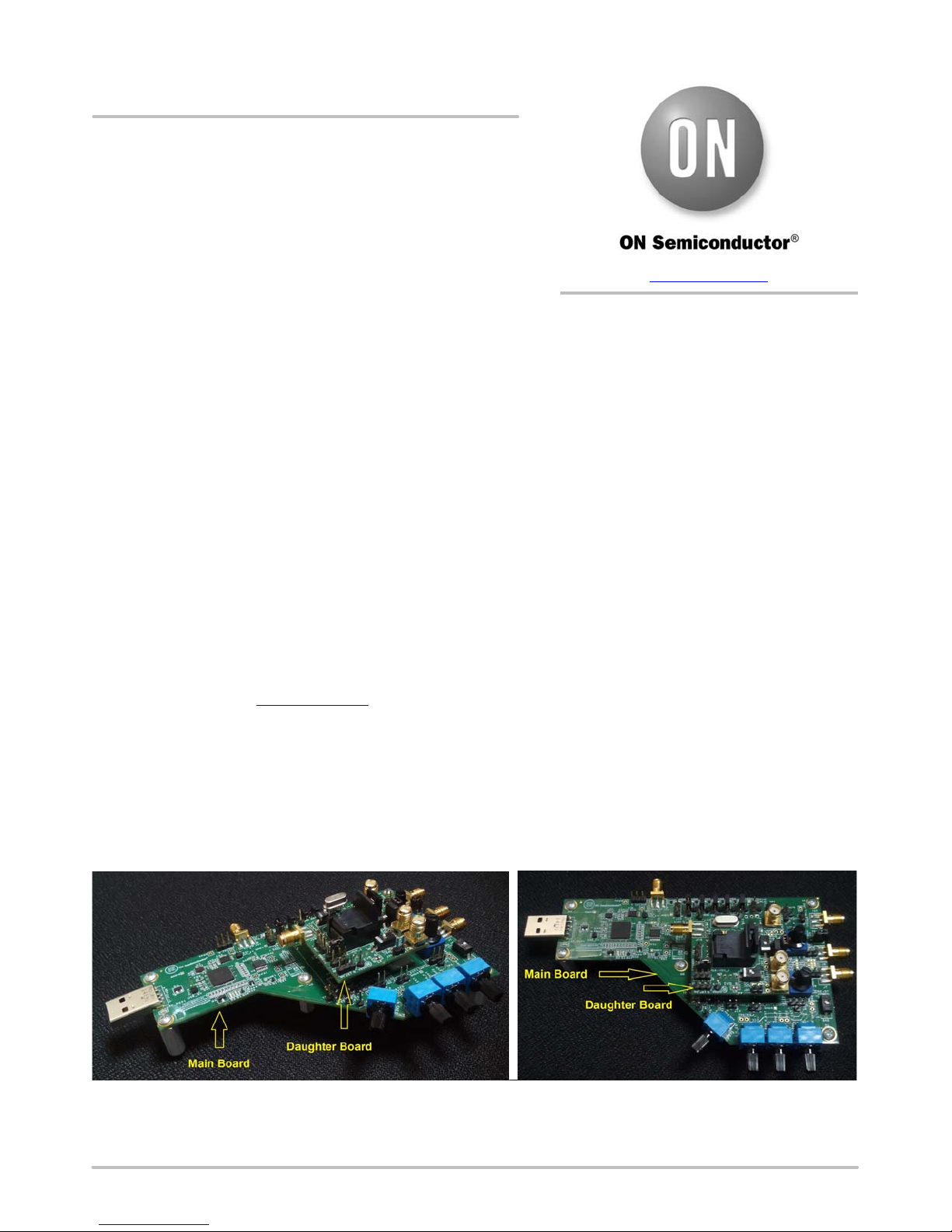
NB3x6x1xxG8DFNEVK is an evaluation kit offering a
convenient solution for evaluating DFN8 devices. Included
are one main board, a daughter board, and a USB cable. The
main board and daughter board are 4 layer boards with
dedicated power and GND planes.
The daughter board plugs directly on to the main board
using four 4−pin header connectors. These connectors route
the signal, power and ground to the device on the daughter
board. The two boards correctly plug into one another in
only one orientation ensuring proper pin alignment. The
daughter board has a DFN8 socket to test NB3x6x1xxG
devices. A view of the main board with the DFN8 daughter
board is shown in Figures 1 and 2.
The Clock Cruiser Software is the GUI software
developed to be used with this evaluation kit, and can be
downloaded for free from www.onsemi.com
user to set programmable parameters and generate solutions
that fit application needs. These solutions can then be
programmed in to device’s OTP memory or be temporarily
written into device registers for evaluation. For more
information on using the GUI, refer to Clock Cruiser User
Guide.
. It allows the
www.onsemi.com
EVAL BOARD USER’S MANUAL
Description
The NB3x6x1xxG, which is a member of the OmniClock
family, is a versatile user programmable clock generator
designed by ON Semiconductor with customer experience
in mind. These devices are tailored to fit into an extensive
array of applications including wearable technology, smart
phones, digital cameras, E−books, portable electronics, and
Internet of Things. The NB3H designated parts are powered
by 3.3 V and 2.5 V supplies while NB3V parts support 1.8
V operation.
These devices are One Time Programmable (OTP), low
power PLL based clock generators that accept fundamental
mode parallel resonant crystals of up to 50 MHz or a single
ended LVCMOS/LVTTL reference clock input of up to
200 MHz. The outputs can be configured as either three
single ended LVCMOS/LVTTL outputs or a combination of
one single ended output and one differential
LVPECL/LVDS/HCSL/CML output. The generated clock
output’s frequency can range between 8 kHz to 200 MHz.
Other programmable parameters include internal crystal
load capacitor, drive strength for LVCMOS outputs, output
frequency modulation controls (type, depth, modulation
rate), output phase inversion, and PLL bypass mode. The
devices are fully functional between −40°C to +85°C.
Figure 1. 455 View of Main Board with DFN8
Daughter Board
© Semiconductor Components Industries, LLC, 2016
July, 2016 − Rev. 1
Figure 2. Top View of Main Board with DFN8
1 Publication Order Number:
EVBUM2358/D
NB3x6x1xxG8DFNEVK
Figure 3. Main Board
Figure 4. DFN8 Daughter Board
www.onsemi.com
2

NB3x6x1xxG8DFNEVK
Step 1: Hardware Setup
Note: Skip this section if device has already been programmed.
Main Board
1. Securely connect the daughter board to the main board by lining up all four 4−pin connectors (J8, J12, J13, J21). The
daughter board can only be plugged in to the main board correctly in one orientation.
2. Make sure all SMA cables are unplugged from main board and daughter board.
3. Jumpers:
a. Use jumpers to provide connection as referenced in table below: (Pin 1 is indicated by a circle)
Jumper No J26 (SEL1) J27 (SEL0) J24 (OE2) J25 (OE1) J28 (OE0) J29 (PD#) J19
Pin connection 2 and 3 2 and 3 2 and 3 2 and 3 2 and 3 OPEN 2 and 3
4. Switches:
b. Slide switches to the position referenced in table below: (ON position is indicated via lettering on switch)
Switch No SW1 SW2
Position ON ON
5. Rotary Switches:
c. Turn knob on rotary switches as shown in table below: (The position number will be displayed in a slit on the knob)
Jumper No U11 U12 U13 U14 U15 U16
Dial Display 1 1 1 1 1 1
Daughter Board
1. Jumpers:
a. Use Jumpers to provide connection as referenced in table below: (Pin 1 is indicated by a circle)
Jumper No J31 (SEL1) J30 (SEL0) J29 (OE2) J28 (OE1) J27 (OE0) J26 (PD#)
Shorting Link Position OPEN OPEN OPEN OPEN OPEN OPEN
2. Switches:
b. Slide switches to the position referenced in table below: (ON position is indicated via lettering on switch)
Switch No SW1 SW2 SW3
Position ON ON ON
3. Ensure that Crystal (XTAL) is in holder.
4. Place NB3H60113G or NB3V60113G in DUT socket U2. For device pin 1 alignment refer to Figure 4.
www.onsemi.com
3
NB3x6x1xxG8DFNEVK
Step 2: Device Programming
Note: Skip this section if device has already been programmed
1. Download and install Clock Cruiser GUI Software to a computer that meets or exceeds minimum requirements found
on Clock Cruiser User guide.
2. Connect the evaluation kit to an USB port using included USB cable. A LED next to the USB connector will glow
red, indicating that +5 V supply has been applied to EVB.
3. Run the Clock Cruiser GUI software. A blue LED (D9) will light up when a connection is established, this LED will
blink periodically as activity is being conducted.
4. Follow the Clock Cruiser User Guide for detailed instructions on navigating through the program to properly
configure device.
5. In the device programming screen, a table indicates the summary of configurations that were selected. Verify that the
Hardware Connected indicator is green and that there is no error in the log.
6. Set appropriate device VDD/VDDO levels.
a. Set VDD and VDDO for each output by using the four rotary switches (U11, U12, U13, and U14) located on the main
board to match device configuration. Make sure that VDDO’s are less than or equal to VDD. The following table shows
which on−board LDO voltage is selected depending on the switch position (see table below).
Voltage for Each Switch Position
Rotary Switch Line
U11 VDD +3.3 V
1 2 3 4
U12 VDDO0
U13 VDDO1
U14 VDDO2
VDD
+2.5 V +1.8 V external source
7. Program the device permanently by selected [Program OTP Memory] or write to device registers by clicking [Write
to Registers]. In the case Write to Register function is utilized, powering down evaluation kit (i.e. unplugging USB
cable) will reset device registers.
Step 3: Device Evaluation
Select Input Clock
Depending on the programmed configuration, select one of the following input clock references.
1. Crystal (XTAL): The evaluation kit comes equipped with a 25 MHz fundamental crystal on the daughter board. If a
different frequency is required, place new crystal in holder. Device can accept 3 MHz to 50 MHz crystal references.
Please follow the additional step below to properly use Crystal as input reference:
a. Place SW1 on daughter board in the OFF position.
2. External Clock Reference: To use an external clock reference, connect external clock to SMA connector J31 on the
main board. Device can accept 3 MHz to 200 MHz clock references, reference device datasheet for appropriate input
levels.
Please follow additional steps below to properly use an external clock input source:
a. Close out GUI software to stop communication between GUI and EVB.
b. Unplug and Re−plug EVB to USB port.
c. Manually supply power to device with PD# pin. (See section Controlling the Device (GPIO pins) for proper use of
PD# pin)
Note: External Clock can only be used with devices that have been OTP’d.
www.onsemi.com
4
NB3x6x1xxG8DFNEVK
Select Output Termination
DUT outputs are routed to three SMA connectors on the main board (J7, J9, and J23) to provide termination for CLK0, CLK1,
and CLK2 respectively. By turning rotary switches U15 and U16, the board will automatically terminate the programmed
output level for CLK0 and CLK1, to its respective output termination in table below.
Rotary Switch
Position
1 LVCMOS LVCMOS
2 HCSL HCSL
3 LVPECL LVPECL
4 CML CML
5 LVDS LVDS
U15 output for CLK0 U16 output for CLK1
Note: CLK2 output only supports LVCMOS levels; therefore its termination is fixed.
Interfacing with Test Equipment
Monitor DUT outputs from main board with an oscilloscope with either SMA connectors or on board jumpers.
1. To use SMA connectors (J7, J9, J23), use oscilloscopes Hi−Z feature or a Hi−Z probe to monitor outputs. (Ensure
probe is properly grounded)
2. To use Jumpers (J33, J34, J35), use a Hi−Z probe connected to jumper pin marked 0. (Ensure probe is properly
grounded)
Both options can be used to monitor all three DUT outputs.
Controlling the Device (GPIO pins)
The device has multiple functions that can be programmed via control pins, below is a list of control pins and their respective
SMA connector.
OE: Pin used to enable or disable outputs individually. The main and daughter boards both have OE pins that can be easily
accessed via jumpers.
Main board: CLK0=J28, CLK1=J25, CLK2=J24
Daughter board: CLK0=J27, CLK1=J28, CLK2=J29
OE
0 CLK Disabled
1 CLK Enabled
Function
PD#: Pin used to power down device, this pin can be controlled either with J29 (main board) or J26 (daughter board). The logic
state of this signal corresponds to the LED (D9) on the main board.
PD#
0 Device Powered Down Off
1 Device Powered Up On
Function LED (D9)
www.onsemi.com
5

NB3x6x1xxG8DFNEVK
SEL: Pin is used to select between the available four output configurations that can be stored in devices OTP memory.
Main board: SEL0=J27, SEL1=J26
Daughter board: SEL0=J30, SEL1=J31
SEL0
L L I
L H II
H L III
H H IV
SEL1 Output Configuration
Programming Reminders
While communicating between the GUI and device ensure the following:
Main Board
1. Switches SW1 and SW2 are set to the ON state.
2. Rotary switches U11, U12, U13, U14, U15 and U16 are in the “1” position.
3. All SMA cables are detached from test equipment.
Daughter Board
1. Switches SW1, SW2 and SW3 are set to the ON position.
2. All SMA cables are detached from test equipment.
When re−configuring temporary device registers ensure the following:
1. Re−initiate main board hardware setup.
2. Re−initiate daughter board hardware setup.
3. Re−initiate GUI by either returning to previous page with [back] button or restarting GUI software.
Note: Even if device OTP memory has been programmed, device registers can be used to write other solutions for evaluation.
www.onsemi.com
6
 Loading...