

Page 1
NB3N1200KMNGEVB,
NB3W1200LMNGEVB
NB3N1200K/NB3W1200L
Evaluation Board
User'sManual
Introduction
The NB3N1200KMNGEVB and the NB3W1200LMNG
EVB evaluation boards were developed with a common
PCB layout design to accommodate the NB3N1200K
(standard HCSL outputs) and the NB3W1200L (HCSL
Push-Pull outputs) devices. Each board comes fully
assembled and tested and is ready to evaluate in the lab. This
evaluation board was designed to provide a flexible and
convenient platform to quickly evaluate, characterize and
verify the operation of the NB3N1200K or NB3W1200L
devices. To minimize the board size, six differential outputs
are accessed with SMA connectors. The other six
differential outputs are loaded, terminated and can be
monitored with ahigh impedance probe as explained later in
the manual.
The NB3N1200K Evaluation Board schematic is the
same as the NB3W1200L schematic except the “1200L” has
some components depopulated (DNI) per the “1200L”
BOM.
http://onsemi.com
EVAL BOARD USER’S MANUAL
• The NB3W1200LMNGEVB does not have RP resistors
installed on its differential Push-Pull outputs.
• The NB3W1200LMNGEVB does not have
FB_OUT/FB_OUT# resistors installed.
• The NB3W1200LMNGEVB does not have R
resistor R107 installed.
This manual should be used in conjunction with the device
datasheet which contains full technical details on the device
specifications and operation.
This evaluation board manual contains:
REF
• Information on the NB3N1200K/NB3W1200L
Evaluation Board
• Assembly Instructions
• Test and Measurement Setup Procedures
• Board Schematic and Bill of Materials
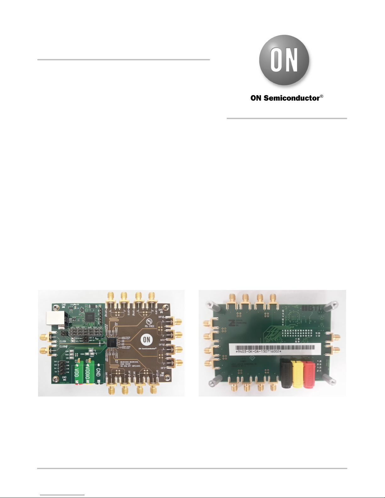
Top View Bottom View
Figure 1. NB3N1200KMNGEVB and NB3W1200LMNGEVB Evaluation Board
© Semiconductor Components Industries, LLC, 2013
December, 2013 − Rev. 0
1 Publication Order Number:
EVBUM2216/D
Page 2
NB3N1200KMNGEVB, NB3W1200LMNGEVB
D
QUICK START LAB SET-UP USER’S GUIDE
Pre-Power-Up
1. The NB3N1200K and NB3W1200L have positive
power supply pins VDD and VDDIO. Connect
power supply cables to VDD, VDDIO and GND
banana jacks; (do not turn power on, yet)
2. Connect a signal generator to the SMA connectors
for the CLK_IN & CLK_IN# inputs.
3. 50-ohm termination resistors are installed for
a signal generator on the board. Set appropriate
input signal levels; (HCSL input, VIL = 0 V,
VIH = 700 mV, Frequency 100 or 133.33 MHz)
4. Ensure the PWRGD/PWRDN# pin is in the Low
state before power up (PWRDN#). There is
a jumper on pin 6 to easily select between High
and Low. See Figure 8.
5. The 100M_133M# and HBW_BYPASS_LBW
pins need to be hardware selected with jumpers.
See Figures 4 and 7.
6. To monitor the DIF_n/DIF_n# outputs, connect the
DIF_n/DIF_n# outputs to the appropriate
oscilloscope.
Table 1. POWER SUPPLY CONNECTIONS
Device Pin
Power Supply Connector
VDD 3.3 V
VDDIO 1.05 V to 3.3 V
GND 0V
Single Power Supply
+3.3 V 0 V
VDD, VDDIO GND
+3.3 V
Figure 2. Power Supply Connections
+3.3 V 0 V
VDD GN
Power Supply
Dual Power Supplies
1.05 V to 3.3 V
VDDIO
1.05 V to 3.3 V
+3.3 V
OscilloscopeSignal Generator
OUT
OUTb
Figure 3. Typical Lab Test Set-Up
Power -Up Sequence
1. Turn on power supply, 3.3 V (VDD & VDDIO).
2. Move PWRGD/PWRDN# jumper from Low to
logic High, PWRGD position.
3. Turn on the Differential Clock Signal for the
CLK_IN inputs. The differential Clock signal for
the CLK_IN inputs can be ON or active before or
after PWRGD is set HIGH.
4. Monitor DIF_n/DIF_n# outputs on oscilloscope.
IN
INb
3.3 V
3.3 V
0 V
Optional
Graphical User Interface
(see page 7)
There is a stand-alone Graphical User Interface software
package and user’s manual that will interface with the DUT
via the USB connector.
1. Connect the USB port on the evaluation board to
a USB port on the PC via cable.
2. See the stand-alone GUI instructions document.
3. Allow Windows to install the necessary drivers for
the eval board USB interface hardware.
4. Start the GUI program.
http://onsemi.com
2
Page 3
NB3N1200KMNGEVB, NB3W1200LMNGEVB
Power Supplies
Each VDD, VDDIO and GND power supply has
a separate side-launch banana jack located on bottom side.
This board is capable of measuring device IDD & IDDIO
separately.
Board Layer #2 = SMA Ground = Device GND = 0 V.
GND Banana Jack = negative power supply for
DUTGND and SMAGND.
Exposed Pad (EP): The exposed pad footprint on the
board is soldered to the exposed pad of the QFN-64
package, and is electrically connected to GND power
supply.
Board Layer #3 = VDD and VDDIO Power Supplies
VDD = positive power supply for core and inputs;
VDD/VDDA/VDDR (pins #1, 8, 24, 40, 57)
VDDIO = positive power supply for outputs; VDDIO
(pins #25, 32, 49, 56)
VDD & VDDIO have the power supply filtering per
datasheet by the banana jacks.
All VDD/VDDA/VDDR/VDDIO device pins have
a 0.1 mF bypass capacitor installed on top side next to
package pins.
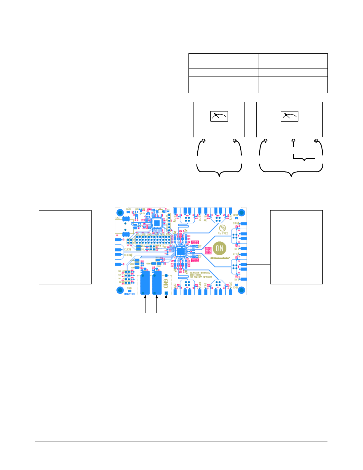
Control Pins
Each control pin can be managed manually with a H/L
jumper header; H = VDD, L = GND.
Tri-Level Input Pins - HBW_BYPASS_LBW#, SA0 and SA1
The three tri-level input pins, HBW_BYPASS_LBW#,
SA0 and SA1, have selectable (with jumper) 4.7 k-ohm
pull-up to VDD and 4.7 k-ohm pull-down to GND resistors;
No jumper defaults to open/float.
• For a HIGH Level – Put Jumper to High
• For a LOW Level − Put Jumper to Low
• For a MID Level − Put Jumper to both High and Low;
this will Enable both Pull-up and Pull-down Resistors
HBW_BYPASS_LBW#
At J65 and J66 headers, there is a 4.7 kW pull-up to VDD
and a 4.7 kW pull-down resistor to GND for manual control.
See Figure 4.
SA0 & SA1
At J67 and J69 headers, there are 4.7 kW pull-ups to VDD
and at J68 and J70, there are 4.7 kW pull-down resistors to
GND for manual control. See Figure 5.
SA0 SA1
VDD
R57
12
4.7K
J65
HBW HI
12
J66
12
HBW LO
HBW
R58
12
4.7K
Figure 4. HBW_BYPASS_LBW# Schematic/PCB Configuration
GND
VDD
GND
VDD
VDD
VDD
R79
12
4.7K
R85
12
4.7K
J67
12
SA0 HI
J69
12
SA1 HI
J68
12
SA0 LO
J70
12
SA1 LO
Figure 5. SA0 & SA1 Schematic/PCB Configuration
5
HBW_BYP_LBW
SA0
R82
12
4.7K
SA1
R88
12
4.7K
11
14
SA0
SA1
http://onsemi.com
3
Page 4
Control Pins (Continued)
NB3N1200KMNGEVB, NB3W1200LMNGEVB
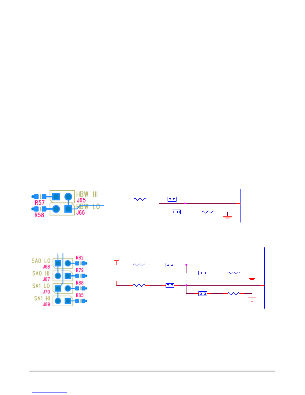
OE_n# Pins (Output Enable/Disable Function)
Six of the twelve differential outputs that have metal
traces going to SMA connectors have OE_n# pins on the left
side of the board that can be controlled manually using the
convenient High/Low OE_n# jumpers. See Figure 6.
OE#
USB GUI
J47
HI − Jumper to VDD
USB − Jumper to Mid
LO − Jumper to GND
Figure 6. OE_n# Pins Schematic/PCB Configuration
100M_133M# - Frequency Selection (J55)
The 100M_133M# frequency selection pin can be
controlled manually with the High/Low header jumper J55,
H = 100 MHz, L = 133 MHz.
All twelve of the OE_n#s can be controlled individually/
automatically by using the software GUI. GUI control is
accomplished via the USB when the OE_n# jumper is
installed on the middle header position. See Figure 6.
37
12
34
56
VDD
OE#
1
J55
2
3
Figure 7. 100M_133M# Pin Schematic/PCB Configuration
PWRGD/PWRDN# (J56)
The PWRGD/PWRDN# pin can be controlled manually
with the High/Low header jumper J56; H = PWRGD,
L = PWRDN#.
1
J56
Figure 8. PWRGD/PWRDN# Pin Schematic/PCB Configuration
2
3
VDD
VDD
4
100M_133M_N
6
PWRGD
http://onsemi.com
4
Page 5

NB3N1200KMNGEVB, NB3W1200LMNGEVB
Differential Clock Inputs and Outputs
CLK_IN & CLK_IN# - Differential Clock Inputs
The differential Clock input traces, CLK_IN/CLK_IN#,
are equal length routed straight from the SMA connectors on
the left side directly to the DUT; there are no vias on metal
traces.
CLK_IN & CLK_IN# have resistor pads (R51 & R52) to
GND to terminate a signal generator, if used. 50-ohm
resistors are installed. Remove these resistors if CLK_IN
& CLK_IN# are driven by another IC device.
Six of the twelve differential outputs are designed to have
equal length metal traces from the device pins to the SMA
connectors.
The other six differential outputs have shortened metal
traces, do not have SMA connectors and can be observed
with a high-impedance probe on the metal pads provided.
Each DIF_n/DIF_n# output has a provision for C
2 pF capacitors are installed on all outputs.
Rs & Rp pads are located close to the DUT . Rs = 33-W is
installed for both the NB3N1200K and NB3W1200L.
NB3N1200K (HCSL Outputs)
DIF_n and DIF_n# - Differential Outputs
NB3N1200KMNGEVB and NB3W1200LMNGEVB
were designed with a flexible PCB layout configuration to
measure the differential HCSL (1200K) or Push-Pull
(1200L) outputs with a 50-ohm scope head or
RP is not installed on the six output pair with long metal
traces to SMA connectors; Use 50-W to GND of the
oscilloscope head for RP.
Rp is installed (50-W to GND) on the short metal traces
without SMA connectors and will use Hi-Z probes.
high-impedance FET probe. (See Output Layout in
Figures 8 and 9)
NB3W1200L (Push-Pull Outputs)
Rp is not installed
Table 2. NB3N1200KMNGEVB AND NB3W1200LMNGEVB OUTPUT LOAD AND TERMINATION
VS. OSCILLOSCOPE MEASUREMENT
Device Output Traces Rs Rp CLoad Scope
1200K Long
1200K Short
1200L Long or Short
33-W
33-W 50-W
33-W
Open (DNI) 2pF
2pF Hi-Z
Open (DNI) 2pF Hi-Z
50-W
Load
;
D IF_4
34
DIF_4
DIF_N4
DIF_5
35
D IF_5
38
DIF_N5
39
DIF_4#
DIF_5#
From: DUT Output
From: DUT Output
R33
12
33
R37
12
33
R41
12
33
R45
12
33
12
1 2
1 2
12
DIF_5#
DIF_5
DIF_4#
DIF_4
R35
49.9
R39
49.9
R43
49.9
R47
49.9
12
C9
2.0pF
12
C10 2.0pF
12 0
C11 2.0pF
1 2
C12 2.0pF
Rs
Rs
OUT4
OUT_N4
Rp
Rp
TP19
TP20
GND
DIF_4
DIF_4#
OUT5
R125
12
R126
12
GND
Long Output Traces:
0
0
PR6
OUT_N5
Use 50-W Scope via SMA Connector
CL
CL is at SMA
Connector
R42
12
R46
12
0
DIF_5#
DIF_5
DIF_4#
Short Output Traces:
Use High-Z Probe
DIF_4
Figure 9. Differential Outputs Schematic/PCB Configuration: Long vs. Short Metal Traces
J11
J12
DIF_5
DIF_5#
http://onsemi.com
5
Page 6

NB3N1200KMNGEVB, NB3W1200LMNGEVB
HCSL Output Measurement
HCSL outputs are typically terminated with 50-W to
ground. Measuring HCSL outputs can be easily
accomplished by:
NB3N1200K (HCSL Outputs) − 50-W Oscilloscope Head
With R
removed from board, connect the HCSL outputs
P
through the SMA connectors to the 50-W internal impedance
of the oscilloscope sampling head.
NB3N1200K (HCSL Outputs) − Use Hi-Z Probe
With R
installed, use a high-impedance probe on the
P
output’s metal trace. Holes for headers to connect to Hi-Z
probes are available, but the header pins are not installed.
• Single-ended Hi-Z probes or,
• Differential Hi-Z probe; (see layout below)
Optional component to Ground, if
needed, when shorted to output trace.
Ground
NB3W1200L (Push-Pull Outputs) − Use Hi-Z Probe
Rp is not installed
• A 0-W series resistor is installed between the end of the
transmission line and the SMA connector. This resistor
can be removed, if needed, to eliminate any SMA
impedance/stub when using Hi-Z probes.
• As a feature, an optional component can be installed on
each output, ie. additional capacitance loading etc.
The following figures describe the boards’ output
features:
C
(2 pF), installed
Load
Series R = 0-W installed
Hi-Z probe
From: DUT Output
Figure 10. Differential Outputs Schematic/PCB Configuration: Use Hi-Z Probe Scope for NB3W1200L
Misc. Pins
FB_OUT & FB_OUT# − External Termination
of Feedback Pins
FB_OUT & FB_OUT# have convenient “test point
anvils” to monitor these pins with Hi-Z probe.
NB3N1200K (HCSL):
Since the FB_OUT & FB_OUT# pins do not drive
transmission lines (no SMAs), the board layout has these
pins loaded/terminated at the DUT per datasheet; 83-W to
GND is installed for the 100-W board.
NB3W1200L (Push-Pull):
FB_OUT & FB_OUT# resistors are not installed.
Short with 0-W resistor for use
with Hi-Z probe; 0-W installed.
IREF Pin
NB3N1200K (HCSL):
The R
resistor (R107) to GND for the HCSL output
REF
part device.
= 475-W is installed for the 100-W board.
R
REF
NB3W1200L (Push-Pull)
R
is not installed for the NB3W1200L device.
REF
http://onsemi.com
6
Page 7

NB3N1200KMNGEVB, NB3W1200LMNGEVB
Graphical User Interface (GUI)
USB & I2C/SMBus Interface
The NB3N1200K EVB has an on-board I
interface circuitry located in the upper left section of the
board.
This circuitry will interface with the software program
and the device via the SDA and SCL input pins, and can
control all twelve of the OE_n# pins, PLL Mode and
Frequency Select directly from the GUI.
SCL & SDA
The SMBus Clock (SCL) and Data (SDA) pins are
exercised through the on-board I
Single Board Design/Layout for NB3N1200K or
NB3W1200L:
2
C interface.
2
C/SMBus
BOARD FEATURES
• The single board design and layout accommodates the
electrical characterization of either the NB3N1200K
(standard HCSL outputs) or the NB3W1200L (HCSL
Push-Pull outputs).
• Incorporates on-board I
powered from a USB connection, minimizing cabling.
2
C/SMBus interface circuitry
• Convenient and compact board layout.
• 3.3 V power supply device operation.
• Differential inputs/outputs signals are accessed via
SMA connectors or high impedance probes.
2
In order to enable the I
jumpers J63 & J64 must be shorted.
2
The I
C/SMBus interface circuitry is powered separately
from the USB type-B connection and is isolated from device
VDD and VDDIO.
The SDA and SCL pins can also be externally accessed by
an off-board programmer , allowing other SMBus emulators
to be used to program the DUT. If used, remove both jumpers
J63 & J64. “Test-point anvils” TP5 & TP6 are available for
external control of the device with the use with mini-grabber
cables.
environment (100-W line-to-line differential) and is
implemented in four layers.
C control of the DUT, header
• All layers are constructed with FR4 dielectric material.
• The first layer is the primary signal layer, including all
of the differential inputs and outputs.
• The second layer is the ground plane. It is dedicated for
the DUT ground/SMA ground plane.
• The third layer is dedicated as the power plane.
rd
A portion of this 3
VDD and VDDIO power planes.
layer is designated for the device
• The fourth layer contains control lines, power supply
banana jacks and device power pin bypass capacitors.
Other Board Features
There are no vias on the high-speed differential I/O metal
traces so as to eliminate via impedance and stub affects.
Board stand-offs are installed.
Board Layout
The NB3N1200K QFN-64 Evaluation Board provides
a high bandwidth, 50-W controlled trace impedance
Figure 11. NB3N1200KMNGEVB and NB3W1200LMNGEVB Evaluation Board Layer Stack-Up
Layer Stack
• L1 (Top) Signal
• L2 Device Ground and SMA Ground
• L3 VDD, VDDIO (Separate Device Power Supplies)
• L4 (Bottom), Power Supply By-pass Capacitors,
Control Pin Traces and Banana Jacks
http://onsemi.com
7
Page 8

NB3N1200KMNGEVB, NB3W1200LMNGEVB
NB3N1200K/NB3W1200L EVALUATION BOARD SCHEMATIC
OUT0
R1
1 2
17
TP15
D IF0
DIF0
DIF1
DIF1#
DIF2
DIF2#
J3
J4
0
0
R10
1 2
1 2
PR2
OUT1
OUT_N1
0
R121
1 2
TP16
OUT_N0
1 2
1 2
1 2
C1 2.0pF
C2 2.0pF
C3 2.0pF
R7
49.9
R11
49.9
49.9
1 2
1 2
33
33
R9
R5
1 2
N0
DIF_
18
DIF_N0
1 2
D IF1
21
R13
1 2
N1
DIF_
22
DIF1
DIF_N1
R3
1 2
33
J6
J5
0
0
0
C4 2.0pF
49.9
1 2
OUT2
R17
1 2
26
D IF2
DIF2
R22
R18
1 2
PR3
OUT_N2
0
0
R124
R123
1 2
1 2
TP17
OUT3
1 2
1 2
C6 2.0pF
C5 2.0pF
49.9
R27
R23
49.9
1 2
33
33
R25
R21
1 2
1 2
N2
DIF_
D IF3
30
27
DIF3
DIF_N2
R19
1 2
33
TP19
TP18
OUT_N3
OUT4
1 2
1 2
C7 2.0pF
C8 2.0pF
R31
49.9
49.9
1 2
1 2
33
R29
R33
1 2
1 2
N3
DIF_
D IF4
34
31
DIF4
DIF_N3
R14
R122
1 2
1 2
R15
1 2
33
DIF5
DIF5#
DIF6
DIF6#
J11
0
1 2
OUT5
TP20
OUT_N4
2.0pF
1 2
1 2
C10
C9 2.0pF
R35
R39
49.9
49.9
1 2
1 2
33
33
R37
R41
1 2
1 2
N4
DIF_
D IF5
38
35
DIF5
DIF_N4
J13
J12
0
R42
1 2
PR6
OUT_N5
0
R125
1 2
2.0pF
1 2
C11
R43
49.9
1 2
33
R45
1 2
N5
DIF_
39
DIF_N5
J14
0
0
R56
R50
R46
1 2
1 2
PR7
OUT_N6
OUT6
0
1 2
D IF6
42
0
R127
R128
1 2
1 2
TP21
TP22
OUT_N7
OUT7
2.0pF
1 2
C13 2.0pF
R53
49.9
1 2
33
R55
DIF6
2.0pF
1 2
1 2
C14
C15
49.9
R67
R63
49.9
1 2
33
33
R61
R65
1 2
1 2
N7
DIF_
D IF7
46
47
DIF7
DIF_N7
R59
1 2
33
1 2
N6
DIF_
43
DIF_N6
TP24
TP23
OUT8
OUT_N8
1 2
1 2
C17 2.0pF
C16 2.0pF
R71
49.9
49.9
1 2
1 2
33
R69
R73
1 2
1 2
N8
DIF_
D IF8
50
51
DIF8
DIF_N8
0
R126
1 2
1 2
C12 2.0pF
R47
49.9
1 2
33
R49
DIF9#
DIF10
DIF9
J20
J19
0
0
R78
1 2
1 2
PR10
OUT_N9
OUT9
0
R129
1 2
1 2
1 2
C18 2.0pF
C19 2.0pF
R75
R80
49.9
49.9
1 2
1 2
33
33
R77
R83
1 2
1 2
N9
DIF_
D IF9
54
55
DIF9
DIF_N9
DIF10#
J21
J22
0
0
R90
0
C20 2.0pF
49.9
1 2
OUT10
R89
1 2
DIF10
59
DIF10
R131
R91
33
1 2
1 2
1 2
PR11
0
C21 2.0pF
49.9
R95
R96
1 2
OUT_N10
0
R132
1 2
1 2
97
1 2
33
1 2
F_N10
DI
60
DIF_N10
OUT11
2.0pF
C23
49.9
R99
1 2
DIF11
63
TP25
TP26
OUT_N11
1 2
1 2
C26 2.0pF
C31 2.0pF
R101
49.9
1 2
33
DIF11
475
R105
49.9
82.5
TP13
R112
1 2
R108
1 2
FBOUT#
0
R113
15
FBOUT_N
82.5
R109
1 2
FBOUT
TP14
0
1 2
16
FBOUT
R107
1 2
1 2
33
R103
1 2
F_N11
DI
64
3
IREF
DIF_N11
R84
R130
1 2
1 2
R86
1 2
33
VDD25VDD
32
TP4
FB2
VDD49VDD
56
IO
VDD
IO
VDD
1 2
J60
2
C37
100nF
1
C36
100nF
1
C35
100nF
1
C34
100nF
1
C33
10uF
10V
1
600
C32
10uF
+
1
VDDIO
GNDA
2
2
2
2
2
10V
GND7GND
GND33GND41GND48GND
65
23
58
EP
2
J61
GND
4.7K
SA0 LO
VDD
VDDR8VDD
VDDA
SA1
1
14
4.7K
R88
1 2
SA1
V DDA
J70
SA1 LO
1 2
TP1
V DDA
1 HI
J69
SA
1 2
R85
4.7K
1 2
R93
1 2
FB1
1 2
J59
VDDR
R94
1 2
2.2
1
VDD
VDD
VDD
24
40
57
VDD
C25
100nF
1
2
10V
1uF
C57
1
2
DR
C30
100nF
VD
1
100nF
1uF
10V
2
C29
100nF
1
2
C28
100nF
2
1
2
2
VDD
TP3
C27
10uF
10V
1
2
TP2
C24
1
C56
1
2.2
600
10V
C22
10uF
+
2
CLKIN_N
49.9
49.9
10
IN_N
CLK
J38
CLKIN#
HBW
HI
J65
HBW
1 2
R57
1 2
VDD
HBW_BYP_LBW5PWRGD
100M_133M_N
4
6
4.7K
R58
1 2
VDD
LO
J66
HBW
1 2
123
J55
4.7K
VDD
123
J56
3 4
OE_IO10
CLKIN
9
62
R52
1 2
R51
1 2
5 6
J52
OE_IO11
IN
CLK
J37
OE_N120OE_N228OE_N329OE_N436OE_N537OE_N644OE_N745OE_N852OE_N953OE_N1061OE_N11
OE_N0
U1
DNI NB3N1200K
19
VDD
VDD
1 2
3 4
5 6
1 2
3 4
5 6
J44
J43
IO2
IO0
OE_
IO3
IO1
OE_
OE_
OE_
VDD
VDD
1 2
3 4
5 6
1 2
3 4
5 6
J48
J47
IO5
IO4
OE_
IO7
IO6
OE_
OE_
OE_
VDD
VDD
1 2
1 2
3 4
5 6
J51
IO9
IO8
OE_
OE_
CLKIN
SA0
SDA12SCL
13
11
R82
1 2
SA0
J68
1 2
0 HI
J67
SA
1 2
R79
4.7K
1 2
VDD
SCL
SDA
OE_IO[0..11]
Figure 12. NB3N1200KMNGEVB & NB3W1200LMNGEVB Board Schematic
http://onsemi.com
8
Page 9

NB3N1200KMNGEVB, NB3W1200LMNGEVB
J62
USB
6
5
123
4
USB
LED1
R115
10nF
1 2
6
2
REF
16V
12K
1
1
1
1%
R118
R117
R116
1 2
R119
1 2
C51
12
59
10K
2
10K
2
10K
2
470
10pF
2
3
4
3V3
FB4
12
600
FB3
24
IO3
OE_
26
IO4
IO5
OE_
OE_
12
1
1
1
1
9
4
VPLL
VPHY
IO6
IO7
OE_
OE_
C41
100nF
1
C40
100nF
1
C39
100nF
1
100nF
C38
1
3V3
20
VCCIO31VCCIO42VCCIO
VCCIO
U2
FT2232H
TCK
16
R111
10K
1
3V3
2
R110
10K
1
2
12
J63
SCL
TP5
C45
100nF
1
VREGIN
SDA
TP6
C44
1
C43
1
C42
1
49
VCORE12VCORE37VCORE
VREGOUT
IO0
IO1
OE_
OE_
100nF
100nF
4.7uF
64
2
2
2
6.3V
2
IO2
OE_
2
2
2
2
56
50
TDI17TDO18TMS19GPIOL021GPIOL122GPIOL223GPIOL3
12
J64
USB_5V
600
C49
100nF
2
4.7uF
6.3V
C48
2
C47
100nF
2
4.7uF
6.3V
C46
2
IO8
IO9
OE_
OE_
GPIOH633GPIOH532GPIOH430GPIOH329GPIOH228GPIOH127GPIOH0
OE_IO10
_DP
USB_DM
USB
7DP8
DM
BDBUS038BDBUS139BDBUS240BDBUS341BDBUS443BDBUS544BDBUS645BDBUS746BCBUS048BCBUS152BCBUS253BCBUS354BCBUS455BCBUS557BCBUS658BCBUS7
GPIOH7
34
OE_IO11
1
004
D1
PACDN
3V3
10K
R114
C50
1 2
1
_RST_N
USB
14
RESET_N
3V3
EECS
63
1
CS
VCC
8
TP7
21
C
2
OSCI
2
7
3V3
TP8
3V3
3.3V
U4
NCP4586,
5V
USB
43
C
Y1
12 MHz
3
OSCO
EECLK62EEDATA
GND
1
61
R120
12
4
3
DIN
CLK
DOUT
GND
NC
NC
6
5
5
1
C53
GND5GND
11
2.2K
1
OUT
IN
1 2
GND15GND25GND35GND47GND
U3
93LC46B
1uF
10V
C59
2
4
NC
GND
2EN3
C58
100nF
1
2
10V
1uF
C55
1
2
10pF
36
60
PWREN_N
SUSPEND_N
51
13
TEST
AGND
10
GND
GND
GND
GND
TP12
TP11
TP10
TP9
SCL
SDA
1
3V3
OE_IO[0..11]
Figure 13. USB Circuitry Schematic
http://onsemi.com
9
C52
100nF
10V
2
Page 10

NB3N1200KMNGEVB, NB3W1200LMNGEVB
Table 3. BILL OF MATERIALS FOR THE NB3N1200KMNGEVB EVALUATION BOARD
Designator Qty. Description Value Tolerance Footprint Manufacturer
B1 1 PC Board,
C1-C21, C23,
C26, C31
C22, C32 2 Capacitor
C24, C25,
C2-C30,
C34-C41,
C43-C45, C47,
C49, C52, C58
C27, C33 2 Capacitor
C42, C46, C48 3 Capacitor
C50 1 Capacitor 10nF 10% 0402 AVX 0402YC103KAT2A Yes Yes
C51, C53 2 Capacitor 10 pF 5% 0402 Murata GRM1555C1H100JZ01D Yes Yes
C55-C57, C59 4 Capacitor
D1 1 ESD
FB1, FB2 2 EMI Filter
FB3, FB4 2 EMI Filter
J3-J6, J11-J14,
J19-J22, J37,
J38
J43, J44, J47,
J48, J51, J52
J56, J55 2 Header Header
J59 1 Banana Jack,
J60 1 Banana Jack,
J61 1 Banana Jack,
J62 1 CONN USB
J63-J70 8 Header Header
LED1 1 LED GREEN
M1-M8, M10,
M12, M14,
M17, M19,
M21, M23-M25
M9, M11, M13,
M15
M16, M18,
M20, M22
R1,R5,R9, R13,
R17, R21, R25,
R29, R33, R37,
R41, R45, R49,
R55, R61, R65,
R69, R73, R77,
R83, R89, R95,
R99, R103
Demo Board
24 Capacitor 2.0 pF 12% 0402 TDK C1005C0G1H020C Yes Yes
20 Capacitor 100 nF 10% 0402 AVX 0402ZD104KAT2A Yes Yes
Suppressor
4 CHANNEL
PROTECTION
Bead
Bead
14 RF Connectors
PC END MT
JCK GLD
.062″
6 Header − − Header
Thru-Hole,
Red
Thru-Hole,
Yellow
Thru-Hole,
Black
TYPE B R/A
HORIZ SMD
CLEAR 0603
SMD
17 CONN
JUMPER
SHORTING
.100″ GOLD
4 STANDOFF
4 Screw,
24 Resistor
4-40
ALUMINUM
5/8″
4-40 x 0.25,
PHP
− − − − − − Yes
10 mF
10 mF
4.7 mF
1 mF
PACDN004 − SOT-143 ON Semiconductor PACDN004SR No Yes
600 W
600 W
− − SMA_END_LA
3-pin
− − CON2_571-050
− − CON2_571-050
− − CON2_571-050
− − SMT USB
2-pin
LED, Green − 0603 LED Lite-On LTST-C190KGKT Yes Yes
Shunt − 2.54 × 5.97
Standoff,
4-40
1/4 × 5/8
− − − Building Fasteners PMS 440 0025 PH Yes Yes
33 W
10% 1206 Vishay TR3A106K010C2000 Yes Yes
20% 0603 TDK C1608X5R1A106M Yes Yes
20% 0402 TDK C1005X5R0J475M Yes Yes
20% 0402 Murata GRM155R61A105ME15D Yes Yes
− 0603 Murata BLM18KG601SN1D Yes Yes
25% 0402 Murata BLM15AG601SN1D Yes Yes
UNCH_0.062″
Thru-Hole 2 × 3
− 3-pin Header,
− 2-pin Header,
− − Keystone 1808 Yes Yes
1% 0402 Panasonic ERJ-2RKF33R0X Yes Yes
thru-hole 0.1
0_DELTRON
0_DELTRON
0_DELTRON
Conn B
thru-hole 0.1
(mm)
Johnson
Components
FCI 67996-206HLF Yes Yes
3M 961103-6404-AR Yes Yes
Deltron 571-0500 Yes Yes
Deltron 571-0700 Yes Yes
Deltron 571-0100 Yes Yes
On Shore
Technology
3M 961102-6404-AR Yes Yes
Sullins QPC02SXGN-RC Yes Yes
Manufacturer
Part Number
142-0701-801 Yes Yes
USB-B1SMHSW6 Yes Yes
Substi-
tution
Allowed
Lead
Free
http://onsemi.com
10
Page 11

NB3N1200KMNGEVB, NB3W1200LMNGEVB
Table 3. BILL OF MATERIALS FOR THE NB3N1200KMNGEVB EVALUATION BOARD (continued)
Designator
R3, R7, R11,
R15, R19, R23,
R27, R31, R35,
R39, R43, R47,
R53, R59, R63,
R67, R71, R75,
R80, R86, R91,
R97, R101,
R105
R10, R14, R18,
R22, R42, R46,
R50, R56, R78,
R84, R90, R96
R51, R52 2 Resistor
R57, R58, R79,
R82, R85, R88
R94, R93 2 Resistor
R107 1 Resistor
R108, R109 2 Resistor
R110, R111,
R114,
R116-R118
R112, R113,
R121-R132
R115 1 Resistor
R119 1 Resistor
R120 1 Resistor
TP1, TP2, TP3,
TP4, TP5, TP6,
TP13, TP14
U1 1 − NB3N1200K − 64-QFN 9 mm ON Semiconductor NB3W1200KMNG No Yes
U2 1 − FT2232H − 64-QFN FTDI FT2232HQ-REEL No Yes
U3 1 − 93LC46B − 8-TSSOP Microchip 93LC46BT-I/ST No Yes
U4 1 − NCP4586,
Y1 1 − 12 MHz − 2.5 × 3.2 (mm)
24 Resistor
12 Resistor
6 Resistor
6 Resistor
14 Resistor
8 Test Point Test Point,
49.9 W
0 W
49.9 W
4.7 kW
2.2 W
475 W
82.5 W
10 kW
0 W
12 kW
470 W
2.2 kW
SMT
3.3 V
1% 0402 Panasonic ERJ-2RKF49R9X Yes Yes
Jumper 0402 Vishay CRCW04020000Z0ED Yes Yes
1% 0603 Panasonic ERJ-3EKF49R9V Yes Yes
5% 0603 Panasonic ERJ-3GEYJ472V Yes Yes
5% 0603 Panasonic ERJ-3GEYJ2R2V Yes Yes
1% 0402 Panasonic ERJ-2RKF4750X Yes Yes
1% 0402 Panasonic ERJ-2RKF82R5X Yes Yes
5% 0402 Panasonic ERJ-2GEJ103X Yes Yes
Jumper 0201 Panasonic ERJ-1GE0R00C Yes Yes
1% 0402 Panasonic ERJ-2RKF1202X Yes Yes
5% 0402 Panasonic ERJ-2GEJ471X Yes Yes
5% 0402 Panasonic ERJ-2GEJ222X Yes Yes
− TP_5015_KEY
− SOT-23-5 ON Semiconductor NCP4586DSN33T1G No Yes
STONE
SMT
ManufacturerFootprintToleranceValueDescriptionQty.
Keystone 5015 Yes Yes
Abracon Corp ABM8G-12.000MHZ-4Y-T3 Yes Yes
Manufacturer
Part Number
Substi-
tution
Allowed
Lead
Free
http://onsemi.com
11
Page 12

NB3N1200KMNGEVB, NB3W1200LMNGEVB
Table 4. BILL OF MATERIALS FOR THE NB3W1200LMNGEVB EVALUATION BOARD
Designator Qty. Description Value Tolerance Footprint Manufacturer
B1 1 PC Board,
C1-C21, C23,
C26, C31
C22, C32 2 Capacitor
C24, C25,
C28-C30,
C34-C41,
C43-C45, C47,
C49, C52, C58
C27, C33 2 Capacitor
C42, C46, C48 3 Capacitor
C50 1 Capacitor 10 nF 10% 0402 AVX 0402YC103KAT2A Yes Yes
C51, C53 2 Capacitor 10 pF 5% 0402 Murata GRM1555C1H100JZ01D Yes Yes
C55-C57, C59 4 Capacitor
D1 1 ESD
FB1, FB2 2 EMI Filter
FB3, FB4 2 EMI Filter
J3-J6, J11-J14,
J19-J22, J37,
J38
J43, J44, J47,
J48, J51, J52
J56, J55 2 Header Header
J59 1 Banana Jack,
J60 1 Banana Jack,
J61 1 Banana Jack,
J62 1 CONN USB
J63-J70 8 Header Header
LED1 1 LED GREEN
M1-M8, M10,
M12, M14,
M17, M19,
M21, M23-M25
M9, M11, M13,
M15
M16, M18,
M20, M22
R1, R5, R9,
R13, R17, R21,
R25, R29, R33,
R37, R41, R45,
R49, R55, R61,
R65, R69, R73,
R77, R83, R89,
R95, R99, R103
Demo Board
24 Capacitor 2.0 pF 12% 0402 TDK C1005C0G1H020C Yes Yes
20 Capacitor 100 nF 10% 0402 AVX 0402ZD104KAT2A Yes Yes
Suppressor
4 CHANNEL
PROTECTION
Bead
Bead
14 RF Connectors
PC END MT
JCK GLD
.062″
6 Header − − Header
Thru-Hole,
Red
Thru-Hole,
Yellow
Thru-Hole,
Black
TYPE B R/A
HORIZ SMD
CLEAR 0603
SMD
17 CONN
JUMPER
SHORTING
.100″ GOLD
4 STANDOFF
4 Screw,
24 Resistor
4-40
ALUMINUM
5/8″
4-40 × 0.25,
PHP
− − − − − − Yes
10 mF
10 mF
4.7 mF
1 mF
PACDN004 − SOT-143 ON Semiconductor PACDN004SR No Yes
600 W
600 W
− − SMA_END_LA
3-pin
− − CON2_571-050
− − CON2_571-050
− − CON2_571-050
− − SMT USB
2-pin
LED, Green − 0603 LED Lite-On LTST-C190KGKT Yes Yes
Shunt − 2.54 × 5.97
Standoff,
4-40
1/4 × 5/8
− − − Building Fasteners PMS 440 0025 PH Yes Yes
33 W
10% 1206 Vishay TR3A106K010C2000 Yes Yes
20% 0603 TDK C1608X5R1A106M Yes Yes
20% 0402 TDK C1005X5R0J475M Yes Yes
20% 0402 Murata GRM155R61A105ME15D Yes Yes
− 0603 Murata BLM18KG601SN1D Yes Yes
25% 0402 Murata BLM15AG601SN1D Yes Yes
UNCH_0.062″
Thru-Hole 2 × 3
− 3-pin Header,
− 2-pin Header,
− − Keystone 1808 Yes Yes
1% 0402 Panasonic ERJ-2RKF33R0X Yes Yes
thru-hole 0.1
0_DELTRON
0_DELTRON
0_DELTRON
Conn B
thru-hole 0.1
(mm)
Johnson
Components
FCI 67996-206HLF Yes Yes
3M 961103-6404-AR Yes Yes
Deltron 571-0500 Yes Yes
Deltron 571-0700 Yes Yes
Deltron 571-0100 Yes Yes
On Shore
Technology
3M 961102-6404-AR Yes Yes
Sullins QPC02SXGN-RC Yes Yes
Manufacturer
Part Number
142-0701-801 Yes Yes
USB-B1SMHSW6 Yes Yes
Substi-
tution
Allowed
Lead
Free
http://onsemi.com
12
Page 13

NB3N1200KMNGEVB, NB3W1200LMNGEVB
P
al
Table 4. BILL OF MATERIALS FOR THE NB3W1200LMNGEVB EVALUATION BOARD (continued)
Designator
R3, R7, R11,
R15, R19, R23,
R27, R31, R35,
R39, R43, R47,
R53, R59, R63,
R67, R71, R75,
R80, R86, R91,
R97, R101,
R105
R10, R14, R18,
R22, R42, R46,
R50, R56, R78,
R84, R90, R96
R51, R52 2 Resistor
R57, R58, R79,
R82, R85, R88
R93, R94 2 Resistor
R107 1 Resistor
R108, R109 0 DNI − − 0402 − − − Yes
R110, R111,
R114,
R116-R118
R112, R113,
R121-R132
R115 1 Resistor
R119 1 Resistor
R120 1 Resistor
TP1-TP6,
TP13, TP14
U1 1 − NB3W1200L − 64-QFN 9 mm ON Semiconductor NB3W1200LMNG No Yes
U2 1 − FT2232H − 64-QFN FTDI FT2232HQ-REEL No Yes
U3 1 − 93LC46B − 8-TSSOP Microchip 93LC46BT-I/ST No Yes
U4 1 − NCP4586,
Y1 1 − 12 MHz − 2.5 × 3.2 (mm)
0 DNI − − 0402 − − − Yes
12 Resistor
6 Resistor
6 Resistor
14 Resistor
8 Test Point Test Point,
0 W
49.9 W
4.7 kW
2.2 W
475 W
10 kW
0 W
12 kW
470 W
2.2 kW
SMT
3.3 V
Jumper 0402 Vishay CRCW04020000Z0ED Yes Yes
1% 0603 Panasonic ERJ-3EKF49R9V Yes Yes
5% 0603 Panasonic ERJ-3GEYJ472V Yes Yes
5% 0603 Panasonic ERJ-3GEYJ2R2V Yes Yes
1% 0402 Panasonic ERJ-2RKF4750X Yes Yes
5% 0402 Panasonic ERJ-2GEJ103X Yes Yes
Jumper 0201 Panasonic ERJ-1GE0R00C Yes Yes
1% 0402 Panasonic ERJ-2RKF1202X Yes Yes
5% 0402 Panasonic ERJ-2GEJ471X Yes Yes
5% 0402 Panasonic ERJ-2GEJ222X Yes Yes
− TP_5015_
− SOT-23-5 ON Semiconductor NCP4586DSN33T1G No Yes
KEYSTONE
SMT
ManufacturerFootprintToleranceValueDescriptionQty.
Keystone 5015 Yes Yes
Abracon Corp ABM8G-12.000MHZ-4Y-T3 Yes Yes
Manufacturer
Part Number
Substi-
tution
Allowed
Lead
Free
ON Semiconductor and are registered trademarks of Semiconductor Components Industries, LLC (SCILLC). SCILLC owns the rights to a number of patents, trademarks,
copyrights, trade secrets, and other intellectual property. A listing of SCILLC’s product/patent coverage may be accessed at www.onsemi.com/site/pdf/Patent−Marking.pdf. SCILLC
reserves the right to m ake c hanges w ithout f urt her n otice t o a ny p roducts h erein. S CILLC m akes n o warrant y, representation or guarantee r egarding t he s uitabilit y of its products for any
particular purpose, nor does SCILLC assume any liability arising out of the application or use of any product or circuit, and specifically disclaims any and all liability, including without
limitation special, consequent ial o r i ncidental d amages. “ Typical” parameters which m ay b e p rovided i n S CILLC d ata s heets a nd/or s pecificat ions c an a nd d o v ary i n d if ferent a pplications
and actual performance may vary over time. All operating parameters, including “Typicals” must be validated for each customer application by customer’s technical experts. SCILLC
does not convey any license under its patent rights nor the r ights of others. SCILLC products are not designed, intended, or authorized for use as components in systems intended for
surgical implant into the b ody, or other applications int ended t o s upport o r s u stain life, or for any ot her a pplicat ion i n w hich t he f ailure o f t he S CILLC p roduct c ould cr eate a s it uation w here
personal injury or death may occur. S hould B uyer p urchase o r u se S CILLC p r oduct s for any such unintended or unauthorized application, Buyer shall indemnify and hold SCILLC and
its officers, e mployees, s ubsidiaries, a f filiates, a nd d istributors h armless a gainst all claims, costs, d amages, a nd e xpenses, a nd r easonable a ttorney fees arising out o f, d irectly o r i ndirect ly,
any claim of personal injury or death associated with such unintended or unauthorized use, even if such claim a lleges t hat SCILLC was negligent regarding the design or manufacture
of the part. SCILLC is an Equal Opportunity/Affirmative Action Employer. This literature is subject to all applicable copyright laws and is not for resale in any manner.
UBLICATION ORDERING INFORMATION
LITERATURE FULFILLMENT:
Literature Distribution Center for ON Semiconductor
P.O. Box 5163, Denver, Colorado 80217 USA
Phone: 303−675−2175 or 800−344−3860 Toll Free USA/Canada
Fax: 303−675−2176 or 800−344−3867 Toll Free USA/Canada
Email: orderlit@onsemi.com
N. American Technical Support: 800−282−9855 Toll Free
USA/Canada
Europe, Middle East and Africa Technical Support:
Phone: 421 33 790 2910
Japan Customer Focus Center
Phone: 81−3−5817−1050
http://onsemi.com
13
ON Semiconductor Website: www.onsemi.com
Order Literature: http://www.onsemi.com/orderlit
For additional information, please contact your loc
Sales Representative
EVBUM2216/D
 Loading...