

Page 1

NB3M8304C
f
3.3 V 200 MHz 1:4
LVCMOS/LVTTL Low Skew
Fanout Buffer
Description
The NB3M8304C is 1:4 fanout buffer with LVCMOS/LVTTL input
and output. The device supports the core supply voltage of 3.3 V (V
pin) and output supply voltage of 2.5 V or 3.3 V (V
V
pin powers the four single ended LVCMOS/LVTTL outputs.
DDO
DDO
DD
pin). The
The NB3M8304C is Form, Fit and Function (pin to pin) compatible
to ICS8304 and ICS8304I. The NB3M8304C is qualified for industrial
operating temperature range.
Features
• Input Clock Frequency up to 200 MHz
• Low Output to Output Skew: 45 ps max
• Low Part to Part Skew: 500 ps max
• Low Additive RMS Phase Jitter
• Input Clock Accepts LVCMOS/ LVTTL Levels
• Operating Voltage:
♦ Core Supply: V
♦ Output Supply: V
= 3.3 V ±5%
DD
= 3.3 V ±5% or 2.5 V ±5%
DDO
• Operating Temperature Range:
♦ Industrial: −40°C to +85°C
• These Devices are Pb−Free and are RoHS Compliant
www.onsemi.com
MARKING
DIAGRAMS*
8
1
SOIC−8
D SUFFIX
CASE 751
A = Assembly Location
L = Wafer Lot
Y = Year
W = Work Week
G = Pb−Free Package
(Note: Microdot may be in either location)
ORDERING INFORMATION
See detailed ordering and shipping information on page 5 o
this data sheet.
8
8304C
ALYWG
G
1
Figure 1. Block Diagram
© Semiconductor Components Industries, LLC, 2014
December, 2014 − Rev. 3
1 Publication Order Number:
NB3M8304C/D
Page 2
NB3M8304C
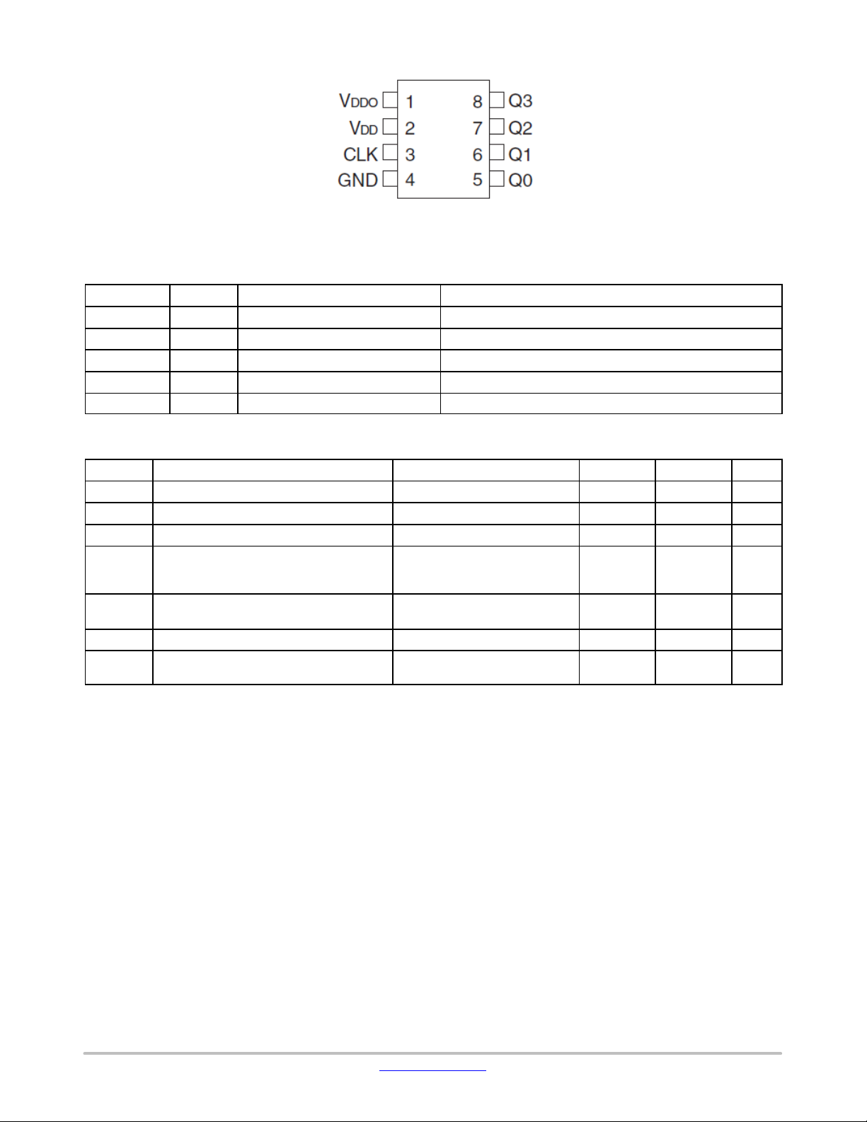
Figure 2. Pin Configuration (Top View)
Table 1. PIN DESCRIPTION
Pin Number Name Type Description
1 VDDO Output Power Clock output Supply pin.
2 VDD Input and Core Power Input and Core Supply pin.
3 CLK LVCMOS/LVTTL Input Clock Input. Internally pull−down.
4 GND Ground Supply Ground.
5, 6, 7, 8 Q[0:3] LVCMOS/LVTTL Output LVCMOS/LVTTL Clock output.
Table 2. MAXIMUM RATINGS
Symbol Parameter Condition Min Max Unit
V
DD, VDDO
V
T
stg
θ
JA
θ
JC
T
sol
MSL Moisture Sensitivity
Stresses exceeding those listed in the Maximum Ratings table may damage the device. If any of these limits are exceeded, device functionality
should not be assumed, damage may occur and reliability may be affected.
1. JEDEC standard multilayer board – 2S2P (2 signal, 2 power)
2. For additional information, see Application Note AND8003/D.
Power Supply − 4.6 V
Input Voltage −0.5 VDD + 0.5 V
I
Storage Temperature −65 +150 °C
Thermal Resistance (Junction−to−Ambient)
SOIC−8
0 lfpm
500 lfpm
Thermal Resistance (Junction to Case)
(Note 1)
Wave Solder 3 sec 265 °C
SOIC−8
Indefinite Time Out of Drypack
(Note 2)
Level 1
80
°C/W
55
12−17 °C/W
www.onsemi.com
2
Page 3
NB3M8304C
Table 3. DC OPERATING CHARACTERISTICS (V
Symbol
R
R
C
C
V
OUT
PD
DD
I
IH
I
IL
Input Pull−down Resistor (CLK Pin) 51
IN
Input Capacitance 4 pF
IN
Output Impedance (Note 3) 5 7 12
Power Dissipation Capacitance (per output) VDD = V
Core Supply Voltage 3.135 3.3 3.465 V
Input High Current VIN = VDD = 3.465 V 150
Input Low Current VDD 3.465 V, VIN = 0.0 V −0.5
3. Outputs terminated with 50W to V
Product parametric performance is indicated in the Electrical Characteristics for the listed test conditions, unless otherwise noted. Product
Parameter Condition Min Typ Max Unit
/2. See Figure 4 for supply considerations.
DDO
= 3.3 V ±5%; TA = −40°C to +85°C)
DD
= 3.465 V 15 pF
DDO
kW
W
mA
mA
performance may not be indicated by the Electrical Characteristics if operated under different conditions.
Table 4. DC OPERATING CHARACTERISTICS (T
Symbol
VDD = 3.3 V +5%, V
V
DDO
V
OH
Output Supply Voltage 2.375 2.625 V
Output HIGH Voltage
DDO
Parameter Condition Min Max Unit
= 2.5 V +5%
= −40°C to +85°C)
A
IOH = −100 mA
2.2 V
IOH = −16 mA 2.1
2.1
2.6
0.2 V
0.5
V
3
0.15
V
0.5
V
OL
VDD = V
V
DDO
V
OH
V
OL
Output LOW Voltage
50 W to V
IOL = 16 mA 0.25
DDO
/2
IOL = 100 mA
= 3.3 V +5%
DDO
50 W to V
DDO
/2
Output Supply Voltage 3.135 3.465 V
Output HIGH Voltage
IOH = −16 mA 2.9
IOH = −100 mA
Output LOW Voltage
50 W to V
IOL = 16 mA 0.25
DDO
/2
IOL = 100 mA
50 W to V
DDO
/2
Table 5. DC OPERATING CHARACTERISTICS
= −40°C to +85°C; VDD = V
(T
A
Symbol
I
DD
I
DDO
V
V
Quiescent Power Supply Current No Load 15 mA
Quiescent Power Supply Current No Load 8 mA
Input HIGH Voltage 2 VDD + 0.3 V
IH
Input LOW Voltage −0.3 1.3 V
IL
= 3.3 V ±5%; VDD = 3.3 V ±5%, V
DDO
Parameter Condition Min Max Unit
= 2.5 V ±5%)
DDO
www.onsemi.com
3
Page 4

NB3M8304C
Table 6. AC CHARACTERISTICS (Note 4)
Symbol
TA = −405C to +855C; VDD = 3.3 V +5%, V
F
t
PLH
t
SKEW
Input Frequency 200 MHz
IN
Propagation Delay (Note 5) Fin = 200 MHz 1.9 3.3 ns
Output to Output Skew(Note 6) 25 45 ps
Part to Part Skew (Note 6) 250 800 ps
t
SKEWDC
Output Duty Cycle (see Figure 3) Fin = 200 MHz 40 60 %
tr/tf Output rise and fall times (Note 7)
TA = −405C to +855C; VDD = 3.3 V +5%, V
F
t
PLH
t
SKEW
Input Frequency 200 MHz
IN
Propagation Delay (Note 5) Fin = 200 MHz 2.2 3.7 ns
Output to Output Skew(Note 6) 25 45 ps
Part to Part Skew (Note 6) 250 500 ps
t
SKEWDC
Output Duty Cycle (see Figure 3) Fin = 200 MHz 40 60 %
tr/tf Output rise and fall times (Note 7)
4. Clock input with 50% duty cycle. Outputs terminated with 50 W to V
5. Measured from V
6. Similar input conditions and the same supply voltages. Measured at V
/2 of the input to V
DD
7. RS is Series Resistance and CL is Load Capacitance at the clock outputs.
NOTE: Device will meet the specifications after thermal equilibrium has been established when mounted in a test socket or printed circuit
board with maintained transverse airflow greater than 500 lfpm. Electrical parameters are guaranteed only over the declared
operating temperature range. Functional operation of the device exceeding these conditions is not implied. Device specification limit
values are applied individually under normal operating conditions and not valid simultaneously.
Parameter Condition Min Typ Max Unit
= 3.3 V +5%
DDO
30% to 70%, RS = 33 W,
250 500 ps
CL = 10 pF
= 2.5 V +5%
DDO
30% to 70%, RS = 33 W,
200 500 ps
CL = 10 pF
/2. See Figures 3 and 4.
/2 of the output.
DDO
DDO
/2. See Figures 3 and 4.
DDO
www.onsemi.com
4
Page 5

NB3M8304C
70%70%
30%30%
Figure 3. AC Reference Measurement
V
DD
NB3M8304C Receiver /
DUT
GND
Spec Condition: TEST SETUP VDD: TEST SETUP V
VDD = V
VDD = 3.3 V ±5%;
V
= 3.3 V ±5% 1.65 V ±5% 1.65 V ±5% −1.65 V ±5%
DDO
= 2.5 V ±5%
DDO
V
DDO
ZO = 50 W
Qx D
50 W
2.05 V ±5% 1.25 V ±5% −1.25 V ±5%
Scope
: TEST SETUP DUT GND:
DDO
Figure 4. Output Driver Typical Device Evaluation and Termination Setup
ORDERING INFORMATION
Device Package Shipping
NB3M8304CDG SOIC−8
(Pb−Free)
NB3M8304CDR2G SOIC−8
(Pb−Free)
†For information on tape and reel specifications, including part orientation and tape sizes, please refer to our Tape and Reel Packaging
Specifications Brochure, BRD8011/D.
98 Units / Rail
2500 / Tape & Reel
†
www.onsemi.com
5
Page 6
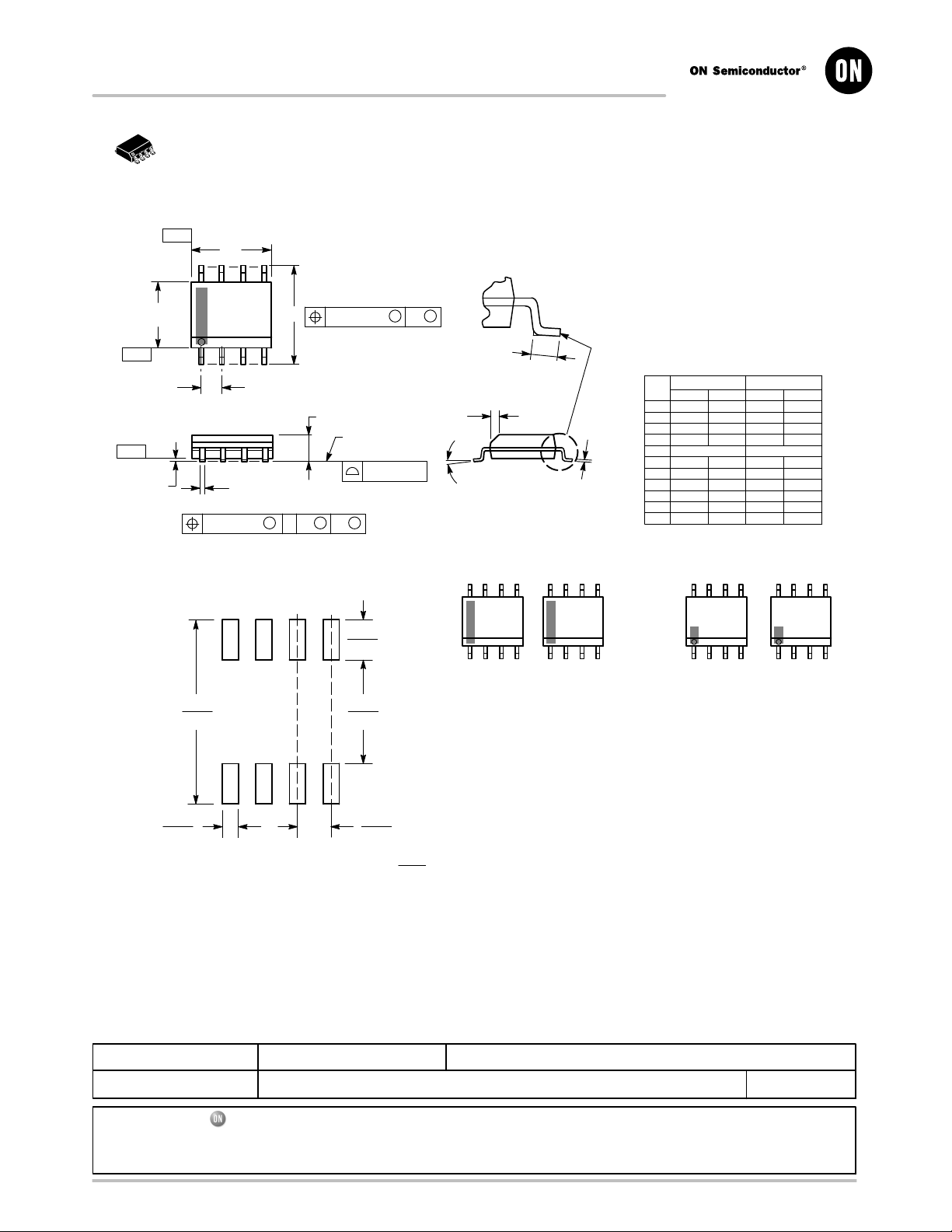
MECHANICAL CASE OUTLINE
PACKAGE DIMENSIONS
8
1
SCALE 1:1
−Y−
−Z−
−X−
A
58
B
1
4
G
H
D
0.25 (0.010) Z
M
SOLDERING FOOTPRINT*
7.0
0.275
S
Y
SXS
0.25 (0.010)
C
SEATING
PLANE
1.52
0.060
0.155
0.10 (0.004)
4.0
CASE 751−07
M
M
Y
N
SOIC−8 NB
ISSUE AK
K
X 45
_
M
J
MARKING DIAGRAM*
8
XXXXX
ALYWX
1
XXXXX = Specific Device Code
A = Assembly Location
L = Wafer Lot
Y = Year
W = Work Week
G = Pb−Free Package
8
XXXXX
ALYWX
G
1
IC
IC
(Pb−Free)
DATE 16 FEB 2011
NOTES:
1. DIMENSIONING AND TOLERANCING PER
ANSI Y14.5M, 1982.
2. CONTROLLING DIMENSION: MILLIMETER.
3. DIMENSION A AND B DO NOT INCLUDE
MOLD PROTRUSION.
4. MAXIMUM MOLD PROTRUSION 0.15 (0.006)
PER SIDE.
5. DIMENSION D DOES NOT INCLUDE DAMBAR
PROTRUSION. ALLOWABLE DAMBAR
PROTRUSION SHALL BE 0.127 (0.005) TOTAL
IN EXCESS OF THE D DIMENSION AT
MAXIMUM MATERIAL CONDITION.
6. 751−01 THRU 751−06 ARE OBSOLETE. NEW
STANDARD IS 751−07.
MILLIMETERS
DIMAMIN MAX MIN MAX
4.80 5.00 0.189 0.197
B 3.80 4.00 0.150 0.157
C 1.35 1.75 0.053 0.069
D 0.33 0.51 0.013 0.020
G 1.27 BSC 0.050 BSC
H 0.10 0.25 0.004 0.010
J 0.19 0.25 0.007 0.010
K 0.40 1.27 0.016 0.050
M 0 8 0 8
____
N 0.25 0.50 0.010 0.020
S 5.80 6.20 0.228 0.244
INCHES
GENERIC
8
XXXXXX
AYWW
1
Discrete
XXXXXX = Specific Device Code
A = Assembly Location
Y = Year
WW = Work Week
G = Pb−Free Package
8
XXXXXX
AYWW
1
Discrete
(Pb−Free)
G
0.6
0.024
1.270
0.050
SCALE 6:1
ǒ
inches
mm
Ǔ
*This information is generic. Please refer to
device data sheet for actual part marking.
Pb−Free indicator, “G” or microdot “G”, may
or may not be present. Some products may
not follow the Generic Marking.
*For additional information on our Pb−Free strategy and soldering
details, please download the ON Semiconductor Soldering and
Mounting Techniques Reference Manual, SOLDERRM/D.
STYLES ON PAGE 2
DOCUMENT NUMBER:
DESCRIPTION:
ON Semiconductor and are trademarks of Semiconductor Components Industries, LLC dba ON Semiconductor or its subsidiaries in the United States and/or other countries.
ON Semiconductor reserves the right to make changes without further notice to any products herein. ON Semiconductor makes no warranty, representation or guarantee regarding
the suitability of its products for any particular purpose, nor does ON Semiconductor assume any liability arising out of the application or use of any product or circuit, and specifically
disclaims any and all liability, including without limitation special, consequential or incidental damages. ON Semiconductor does not convey any license under its patent rights nor the
rights of others.
© Semiconductor Components Industries, LLC, 2019
98ASB42564B
SOIC−8 NB
Electronic versions are uncontrolled except when accessed directly from the Document Repository.
Printed versions are uncontrolled except when stamped “CONTROLLED COPY” in red.
PAGE 1 OF 2
www.onsemi.com
Page 7
STYLE 1:
PIN 1. EMITTER
2. COLLECTOR
3. COLLECTOR
4. EMITTER
5. EMITTER
6. BASE
7. BASE
8. EMITTER
STYLE 5:
PIN 1. DRAIN
2. DRAIN
3. DRAIN
4. DRAIN
5. GATE
6. GATE
7. SOURCE
8. SOURCE
STYLE 9:
PIN 1. EMITTER, COMMON
2. COLLECTOR, DIE #1
3. COLLECTOR, DIE #2
4. EMITTER, COMMON
5. EMITTER, COMMON
6. BASE, DIE #2
7. BASE, DIE #1
8. EMITTER, COMMON
STYLE 13:
PIN 1. N.C.
2. SOURCE
3. SOURCE
4. GATE
5. DRAIN
6. DRAIN
7. DRAIN
8. DRAIN
STYLE 17:
PIN 1. VCC
2. V2OUT
3. V1OUT
4. TXE
5. RXE
6. VEE
7. GND
8. ACC
STYLE 21:
PIN 1. CATHODE 1
2. CATHODE 2
3. CATHODE 3
4. CATHODE 4
5. CATHODE 5
6. COMMON ANODE
7. COMMON ANODE
8. CATHODE 6
STYLE 25:
PIN 1. VIN
2. N/C
3. REXT
4. GND
5. IOUT
6. IOUT
7. IOUT
8. IOUT
STYLE 29:
PIN 1. BASE, DIE #1
2. EMITTER, #1
3. BASE, #2
4. EMITTER, #2
5. COLLECTOR, #2
6. COLLECTOR, #2
7. COLLECTOR, #1
8. COLLECTOR, #1
STYLE 2:
PIN 1. COLLECTOR, DIE, #1
2. COLLECTOR, #1
3. COLLECTOR, #2
4. COLLECTOR, #2
5. BASE, #2
6. EMITTER, #2
7. BASE, #1
8. EMITTER, #1
STYLE 6:
PIN 1. SOURCE
2. DRAIN
3. DRAIN
4. SOURCE
5. SOURCE
6. GATE
7. GATE
8. SOURCE
STYLE 10:
PIN 1. GROUND
2. BIAS 1
3. OUTPUT
4. GROUND
5. GROUND
6. BIAS 2
7. INPUT
8. GROUND
STYLE 14:
PIN 1. N−SOURCE
2. N−GATE
3. P−SOURCE
4. P−GATE
5. P−DRAIN
6. P−DRAIN
7. N−DRAIN
8. N−DRAIN
STYLE 18:
PIN 1. ANODE
2. ANODE
3. SOURCE
4. GATE
5. DRAIN
6. DRAIN
7. CATHODE
8. CATHODE
STYLE 22:
PIN 1. I/O LINE 1
2. COMMON CATHODE/VCC
3. COMMON CATHODE/VCC
4. I/O LINE 3
5. COMMON ANODE/GND
6. I/O LINE 4
7. I/O LINE 5
8. COMMON ANODE/GND
STYLE 26:
PIN 1. GND
2. dv/dt
3. ENABLE
4. ILIMIT
5. SOURCE
6. SOURCE
7. SOURCE
8. VCC
STYLE 30:
PIN 1. DRAIN 1
2. DRAIN 1
3. GATE 2
4. SOURCE 2
5. SOURCE 1/DRAIN 2
6. SOURCE 1/DRAIN 2
7. SOURCE 1/DRAIN 2
8. GATE 1
SOIC−8 NB
CASE 751−07
ISSUE AK
STYLE 3:
STYLE 7:
STYLE 11:
STYLE 15:
STYLE 19:
STYLE 23:
PIN 1. DRAIN, DIE #1
2. DRAIN, #1
3. DRAIN, #2
4. DRAIN, #2
5. GATE, #2
6. SOURCE, #2
7. GATE, #1
8. SOURCE, #1
PIN 1. INPUT
2. EXTERNAL BYPASS
3. THIRD STAGE SOURCE
4. GROUND
5. DRAIN
6. GATE 3
7. SECOND STAGE Vd
8. FIRST STAGE Vd
PIN 1. SOURCE 1
2. GATE 1
3. SOURCE 2
4. GATE 2
5. DRAIN 2
6. DRAIN 2
7. DRAIN 1
8. DRAIN 1
PIN 1. ANODE 1
2. ANODE 1
3. ANODE 1
4. ANODE 1
5. CATHODE, COMMON
6. CATHODE, COMMON
7. CATHODE, COMMON
8. CATHODE, COMMON
PIN 1. SOURCE 1
2. GATE 1
3. SOURCE 2
4. GATE 2
5. DRAIN 2
6. MIRROR 2
7. DRAIN 1
8. MIRROR 1
PIN 1. LINE 1 IN
2. COMMON ANODE/GND
3. COMMON ANODE/GND
4. LINE 2 IN
5. LINE 2 OUT
6. COMMON ANODE/GND
7. COMMON ANODE/GND
8. LINE 1 OUT
STYLE 27:
PIN 1. ILIMIT
2. OVLO
3. UVLO
4. INPUT+
5. SOURCE
6. SOURCE
7. SOURCE
8. DRAIN
DATE 16 FEB 2011
STYLE 4:
PIN 1. ANODE
2. ANODE
3. ANODE
4. ANODE
5. ANODE
6. ANODE
7. ANODE
8. COMMON CATHODE
STYLE 8:
PIN 1. COLLECTOR, DIE #1
2. BASE, #1
3. BASE, #2
4. COLLECTOR, #2
5. COLLECTOR, #2
6. EMITTER, #2
7. EMITTER, #1
8. COLLECTOR, #1
STYLE 12:
PIN 1. SOURCE
2. SOURCE
3. SOURCE
4. GATE
5. DRAIN
6. DRAIN
7. DRAIN
8. DRAIN
STYLE 16:
PIN 1. EMITTER, DIE #1
2. BASE, DIE #1
3. EMITTER, DIE #2
4. BASE, DIE #2
5. COLLECTOR, DIE #2
6. COLLECTOR, DIE #2
7. COLLECTOR, DIE #1
8. COLLECTOR, DIE #1
STYLE 20:
PIN 1. SOURCE (N)
2. GATE (N)
3. SOURCE (P)
4. GATE (P)
5. DRAIN
6. DRAIN
7. DRAIN
8. DRAIN
STYLE 24:
PIN 1. BASE
2. EMITTER
3. COLLECTOR/ANODE
4. COLLECTOR/ANODE
5. CATHODE
6. CATHODE
7. COLLECTOR/ANODE
8. COLLECTOR/ANODE
STYLE 28:
PIN 1. SW_TO_GND
2. DASIC_OFF
3. DASIC_SW_DET
4. GND
5. V_MON
6. VBULK
7. VBULK
8. VIN
DOCUMENT NUMBER:
DESCRIPTION:
ON Semiconductor and are trademarks of Semiconductor Components Industries, LLC dba ON Semiconductor or its subsidiaries in the United States and/or other countries.
ON Semiconductor reserves the right to make changes without further notice to any products herein. ON Semiconductor makes no warranty, representation or guarantee regarding
the suitability of its products for any particular purpose, nor does ON Semiconductor assume any liability arising out of the application or use of any product or circuit, and specifically
disclaims any and all liability, including without limitation special, consequential or incidental damages. ON Semiconductor does not convey any license under its patent rights nor the
rights of others.
© Semiconductor Components Industries, LLC, 2019
98ASB42564B
SOIC−8 NB
Electronic versions are uncontrolled except when accessed directly from the Document Repository.
Printed versions are uncontrolled except when stamped “CONTROLLED COPY” in red.
PAGE 2 OF 2
www.onsemi.com
Page 8
ON Semiconductor and are trademarks of Semiconductor Components Industries, LLC dba ON Semiconductor or its subsidiaries in the United States and/or other countries.
ON Semiconductor owns the rights to a number of patents, trademarks, copyrights, trade secrets, and other intellectual property. A listing of ON Semiconductor’s product/patent
coverage may be accessed at www.onsemi.com/site/pdf/Patent−Marking.pdf
ON Semiconductor makes no warranty, representation or guarantee regarding the suitability of its products for any particular purpose, nor does ON Semiconductor assume any liability
arising out of the application or use of any product or circuit, and specifically disclaims any and all liability, including without limitation special, consequential or incidental damages.
Buyer is responsible for its products and applications using ON Semiconductor products, including compliance with all laws, regulations and safety requirements or standards,
regardless of any support or applications information provided by ON Semiconductor. “Typical” parameters which may be provided in ON Semiconductor data sheets and/or
specifications can and do vary in different applications and actual performance may vary over time. All operating parameters, including “Typicals” must be validated for each customer
application by customer’s technical experts. ON Semiconductor does not convey any license under its patent rights nor the rights of others. ON Semiconductor products are not
designed, intended, or authorized for use as a critical component in life support systems or any FDA Class 3 medical devices or medical devices with a same or similar classification
in a foreign jurisdiction or any devices intended for implantation in the human body. Should Buyer purchase or use ON Semiconductor products for any such unintended or unauthorized
application, Buyer shall indemnify and hold ON Semiconductor and its officers, employees, subsidiaries, affiliates, and distributors harmless against all claims, costs, damages, and
expenses, and reasonable attorney fees arising out of, directly or indirectly, any claim of personal injury or death associated with such unintended or unauthorized use, even if such
claim alleges that ON Semiconductor was negligent regarding the design or manufacture of the part. ON Semiconductor is an Equal Opportunity/Affirmative Action Employer. This
literature is subject to all applicable copyright laws and is not for resale in any manner.
. ON Semiconductor reserves the right to make changes without further notice to any products herein.
PUBLICATION ORDERING INFORMATION
LITERATURE FULFILLMENT:
Email Requests to: orderlit@onsemi.com
ON Semiconductor Website: www.onsemi.com
TECHNICAL SUPPORT
North American Technical Support:
Voice Mail: 1 800−282−9855 Toll Free USA/Canada
Phone: 011 421 33 790 2910
Europe, Middle East and Africa Technical Support:
Phone: 00421 33 790 2910
For additional information, please contact your local Sales Representative
◊
www.onsemi.com
1
 Loading...