

Page 1
NB3L208KMNGEVB
NB3L208K
Evaluation Board
User's Manual
Introduction
The NB3L208K is a differential 1:8 Clock fanout buffer
with High-speed Current Steering Logic (HCSL) outputs.
Inputs can directly accept differential LVPECL, LVDS and
HCSL signals. Single-ended LVPECL, HCSL, LVCMOS,
or LVTTL levels are accepted with a proper external V
reference supply. These signals will be translated to HCSL
and eight identical copies of Clock will be distributed,
operating up to 350 MHz.
This manual should be used in conjunction with the device
datasheet, which contains full technical details on the device
specifications and operation.
TH
www.onsemi.com
EVAL BOARD USER’S MANUAL
This evaluation board manual contains:
• Information on the NB3L208K Evaluation Board
• Block Diagram and Board Schematic
• Assembly Instructions
• Test and Measurement Setup Procedures
• Bill of Materials
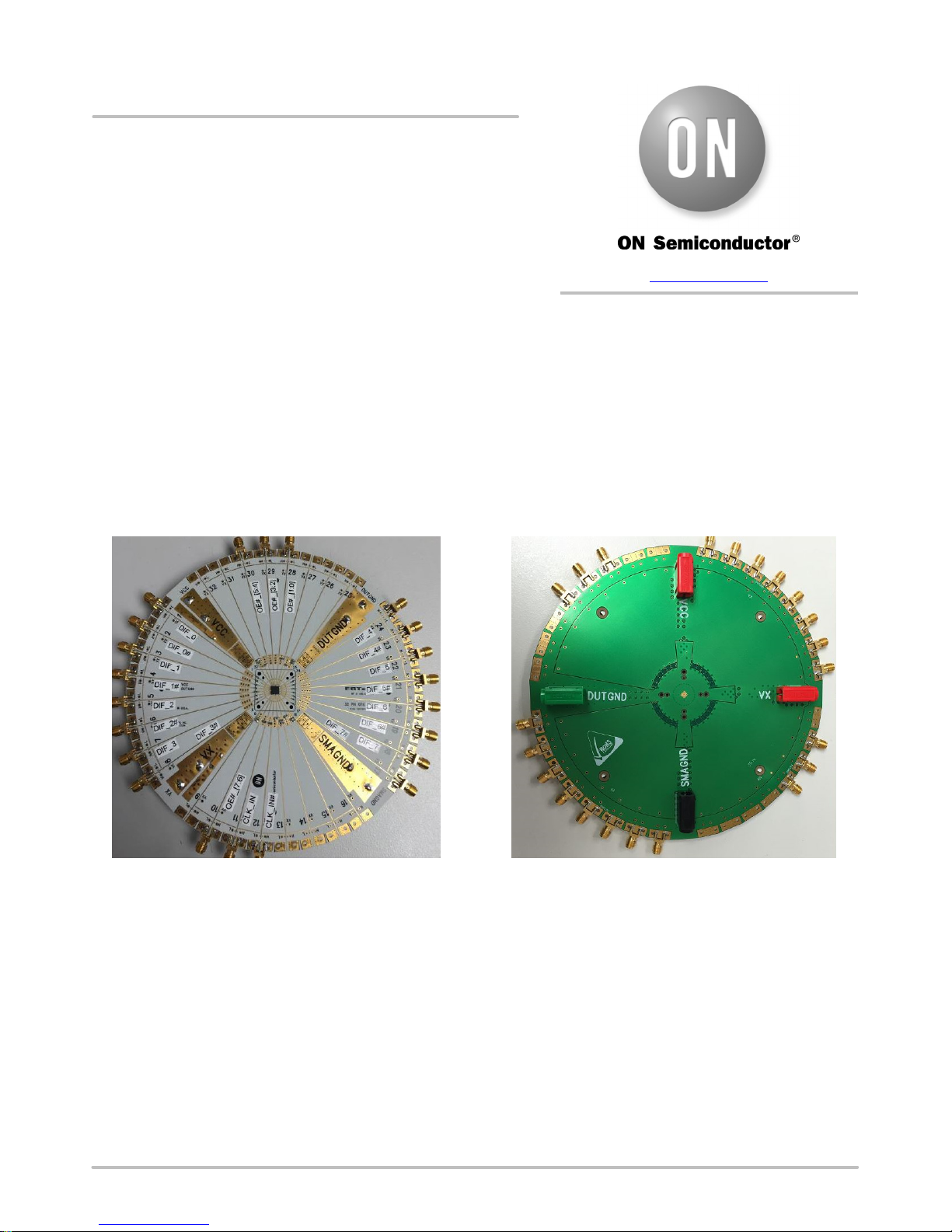
Top View Bottom View
Figure 1. NB3L208KMNGEVB Top and Bottom View
© Semiconductor Components Industries, LLC, 2016
April, 2016 − Rev. 1
1 Publication Order Number:
EVBUM2295/D
Page 2

Equipment Required
1. DC Power Supply
2. Oscilloscope
3. Phase Noise Analyzer
4. Connectors for DC Power Supply
5. 50-W SMA Connectors for I/Os
Block Diagram
Power Supply
NB3L208KMNGEVB
QUICK START LAB SET-UP USER’S GUIDE
VDD GND
VDD GND
Note: Balun Connected to Outputs Only during Phase Noise Testing.
CLK_IN CLK_IN
NB3L208K
Generator Tek DPO70404Agilent E5052B
DIF_0−7
DIF_0−7#
DIF_0−7
DIF_0−7#
Figure 2. Time and Frequency Domain Block Diagram
Power Supplies
Each VDD, VDD_0 (VX on board), GND_0 (DUTGND
on board) and SMAGND power supply has a separate
side-launch banana jack located on bottom side of the test
board (as shown in Figure 1).
SSA Signal
Source Analyzer
Balun
CH1 CH2 CH3 CH4
HCSL Outputs
HCSL outputs are typically loaded and terminated with
a series resist o r ( R
) = 33-W and 50-W to ground. This
SERIES
can be easily accomplished by connecting the HCSL outputs
to the 50-W internal impedance in the oscilloscope. There
are on-board R
= 33-W termination resistors installed
SERIES
for each HCSL output.
R
= 33 W
SERIES
50 W to Ground via
SMA Connector to
Oscilloscope
Figure 3. Set-Up for HCSL Output
www.onsemi.com
2
Page 3

NB3L208KMNGEVB
SMAGNDSMAGNDSMAGND
R1 50 W
SMAGND
SMAGND
R2 50 W
C1 0.1 mF
C2 0.1 mF
C3 0.1 mF
SMAGND
10
11
12
13
14
15
16
9
SMAGND
VDD_0
OE#_[7:6]
CLK_IN
CLK_IN#
GND
VDD
GND_0
VDD_0
SMAGND
33 W
33 W
7
8
DIF_3
DIF_3#
DIF_2#
EP TIED TO
DUT GND
SMAGND
33 W
33 W
5
6
DIF_2
33 W
4
DIF_1
DIF_1#
SMAGND
33 W
33 W
2
3
DIF_0#
GND_0
OE#_[5:4]
OE#_[3:2]
OE#_[1:0]
GND_0
33 W
1
DIF_0
VDD_0
IREF
VDD_0
SMAGND
C5 0.1 mF
32
31
30
29
28
R3 475 W
27
26
25
C4 0.1 mF
SMAGND
SMAGND
SMAGNDSMAGNDSMAGND
SMAGND
SMAGND
SMAGND
DIF_7#
DIF_7
DIF_6#
DIF_6
DIF_5#
DIF_5
DIF_4#
22
21
20
19
18
17
33 W
33 W
33 W
33 W
33 W
C6
10 mF
SMAGND
SMAGND
33 W
SMAGND
SMAGND
Figure 4. NB3L208KEVB Schematic
www.onsemi.com
3
DIF_4
24
23
33 W
33 W
SMAGND
SMAGND
SMAGND
Page 4

NB3L208KMNGEVB
Test and Measurement Setup Procedures
1. Connect VDD and VDD_0 (VX on board) of
the NB3L208K to DC source with power supply
cables (do not turn power on, yet).
2. Connect SMAGND and DUTGND to
the appropriate DC source. For differential HCSL
inputs, both SMAGND and DUTGND are
connected together.
3. Connect the outputs of the generator to
the CLK_IN & CLK_IN# inputs with 50-W
connectors. For phase noise test, low noise
generator is required to ensure the best additive
RMS Phase jitter of the DUT.
4. Connect the DIF_n/DIF_n# outputs to the
appropriate oscilloscope channel. The board does
not have 50-W output termination, thus use of the
probes with 50-W termination is required.
Power-Up Sequence
1. Turn on DUT power supply.
2. Setup the generator V
, VIL levels to set up
IH
the inputs to desired inputs levels, i.e differential
LVPECL, LVDS, and HCSL signals or
Single-ended LVPECL, HCSL, LVCMOS,
or LVTTL. For differential HCSL inputs,
V
= 0 V and VIH = 700 mV.
IL
3. Monitor DIF_n/DIF_n# outputs on oscilloscope.
www.onsemi.com
4
Page 5

NB3L208KMNGEVB
P
al
BILL OF MATERIALS
Table 1. NB3L208KMNGEVB BILL OF MATERIALS
Component Qty. Description Manufacturer Part Number Web Site
SMA Connector 22 Edge Mount Johnson 142−0711−821
Banana Jack Connector 2 Red − Side Launch Deltron 571−0500 Mouser #164−6219
Banana Jack Connector 1 Black − Side Launch Deltron 571−0100 Mouser #164−6218
Banana Jack Connector 1 Green − Side Launch Deltron Mouser
Chip Resistor 9
Chip Resistor 16
Chip Resistor 4
Chip Resistor 1
Capacitor 2
Chip Capacitor 5
Stand-Off 4 Standoff, 4−40 1/4 × 5/8 Keystone 1808 Digi-Key
Screw 4 Screw, 4−40 × 0.25, PHP Building Fasteners PMS 440 0025 PH Digi-Key
Evaluation Board 1 NB3L208KEVB
Device Under Test 1 DUT ON Semiconductor NB3L208K www.onsemi.com
10 mF ±10%, Case “C” 25 V or 16 V
0-Q 0603
33-Q 0402
50-Q, 0603
475-Q 0603
0.1 mF ±10%, 0603
QFN−32 Evaluation Board
NOTE: Components are available through most distributors, i.e. www.newark.com, www.Digikey.com.
Vishay CRCW06030000Z0EA Digi-Key
Panasonic ERJ−2RKF33R0X Digi-Key
Vishay FC0603E50R0BTBST1 Digi-Key
Vishay TNPW0603475RBEEA Digi-Key
KEMET T491C106K025AT
AVX 0603C104KAT2A
ON Semiconductor NB3L208KEVB
T491C106K016AS
541−0.0GTR−ND
ERJ−2RKF33R0X
FC0603−50BFTR−ND
541−2027−2−ND
478−1129−1−ND
www.avx.com
Digi-Key
1808K−ND
H342−ND
ON Semiconductor and the are registered trademarks of Semiconductor Components Industries, LLC (SCILLC) or its subsidiaries in the United States and/or other countries.
SCILLC owns the rights to a number of patents, trademarks, copyrights, trade secrets, and other intellectual property. A listing of SCILLC’s product/patent coverage may be accessed
at www.onsemi.com/site/pdf/ Patent− Marking.pdf . S CILLC reserves t he right to m ake changes wit hout further notice to any products h erein. SCILLC makes no warranty, representation
or guarantee regarding the suitability of its products for any particular purpose, nor does SCILLC assume any liability arising out of the application or use of any product or circuit, and
specifically disclaims any and all liability, including without limitation special, consequential or incidental damages. “Typical” parameters which may be provided in SCILLC data sheets
and/or specifications can and do vary in different applications and actual performance may vary over time. All operating parameters, including “Typicals” must be validated for each
customer application by customer’s technical e xperts. SCILLC does not convey any license under i t s p atent r ights n or t he r ights o f o t hers. S CILLC p roduct s a re n ot d esigned, i nt ended,
or authorized for use as components in systems intended for surgic al i mplant into the body, or other applications intended to support or sustain life, or for any other application in which
the failure of the SCILLC product could create a situation where personal injury or death may occur. Should Buyer purchase or use SCILLC products for any such unintended or
unauthorized application, Buyer shall indemnify and hold SCILLC and its officers, em ployees, subsidiaries, affiliates, and distributors harmless against all claims, costs, damages, and
expenses, and reasonable at torney f ees a r ising o ut o f, d irectly o r indirectly, any claim o f p ersonal i njury o r d eath a ssociated w ith s uch u nint ended o r u nauthorized u se, e ven if such claim
alleges that SCILLC was negligent r egarding the design o r manuf acture o f t he p art. SCILLC is an E qual O pportunity/Af firmative Act ion Employer. This literature is s ubject t o a ll applicable
copyright laws and is not for resale in any manner.
UBLICATION ORDERING INFORMATION
LITERATURE FULFILLMENT:
Literature Distribution Center for ON Semiconductor
19521 E. 32nd Pkwy, Aurora, Colorado 80011 USA
Phone: 303−675−2175 or 800−344−3860 Toll Free USA/Canada
Fax: 303−675−2176 or 800−344−3867 Toll Free USA/Canada
Email: orderlit@onsemi.com
N. American Technical Support: 800−282−9855 Toll Free
USA/Canada
Europe, Middle East and Africa Technical Support:
Phone: 421 33 790 2910
Japan Customer Focus Center
Phone: 81−3−5817−1050
www.onsemi.com
5
ON Semiconductor Website: www.onsemi.com
Order Literature: http://www.onsemi.com/orderlit
For additional information, please contact your loc
Sales Representative
EVBUM2295/D
Page 6

Mouser Electronics
Authorized Distributor
Click to View Pricing, Inventory, Delivery & Lifecycle Information:
ON Semiconductor:
NB3L208KMNGEVB
 Loading...