

Page 1
NB2305A
3.3 V Zero Delay
Clock Buffer
The NB2305A is a versatile, 3.3 V zero delay buffer designed to
distribute high−speed clocks. It accepts one reference input and drives
out five low−skew clocks. It is available in a 8 pin package.
The −1H version of the NB2305A operates at up to 133 MHz, and
has higher drive than the −1 devices. All parts have on−chip PLL’s that
lock to an input clock on the REF pin. The PLL feedback is on−chip
and is obtained from the CLKOUT pad.
Multiple NB2305A devices can accept the same input clock and
distribute it. In this case the skew between the outputs of the two
devices is guaranteed to be less than 700 ps.
All outputs have less than 200 ps of cycle−to−cycle jitter. The input
and output propagation delay is guaranteed to be less than 350 ps, and
the output to output skew is guaranteed to be less than 250 ps.
The NB2305A is available in two different configurations, as shown
in the ordering information table. The NB2305AI is the base part. The
NB2305AI1H is the high drive version of the −1 and its rise and fall
times are much faster than −1 part.
Features
• 15 MHz to 133 MHz Operating Range, Compatible with CPU and
PCI Bus Frequencies
• Zero Input − Output Propagation Delay
• Multiple Low−Skew Outputs
• Output−Output Skew Less than 250 ps
• Device−Device Skew Less than 700 ps
• One Input Drives 5 Outputs
• Less than 200 ps Cycle−to−Cycle Jitter is Compatible with PentiumR
Based Systems
• Accepts Spread Spectrum Clock at the Input
• Available in 8 Pin, 150 mil SOIC Package and 8 Pin TSSOP 4.4 mm
• 3.3 V Operation, Advanced 0.35 CMOS Technology
• Guaranteed Across Commercial and Industrial Temperature Ranges
• These are Pb−Free Devices
www.
onsemi.com
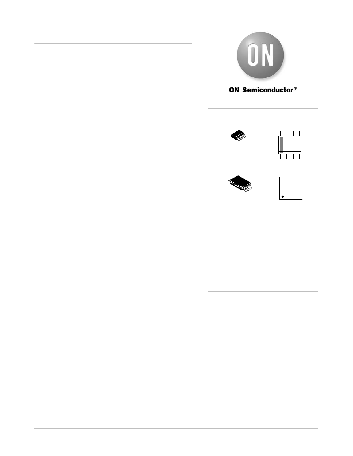
MARKING
DIAGRAMS*
8
1
SOIC−8
D SUFFIX
CASE 751
8
1
TSSOP−8
DT SUFFIX
CASE 948S
XXXX = Device Code
A = Assembly Location
L = Wafer Lot
Y = Year
W = Work Week
G = Pb−Free Package
*For additional marking information, refer to
Application Note AND8002/D.
ORDERING INFORMATION
See detailed ordering, marking and shipping information in the
package dimensions section on page 6 of this data sheet.
8
XXXX
ALYW
G
1
8
XXX
YWW
A G
1
© Semiconductor Components Industries, LLC, 2015
May, 2015 − Rev. 11
1 Publication Order Number:
NB2305A/D
Page 2
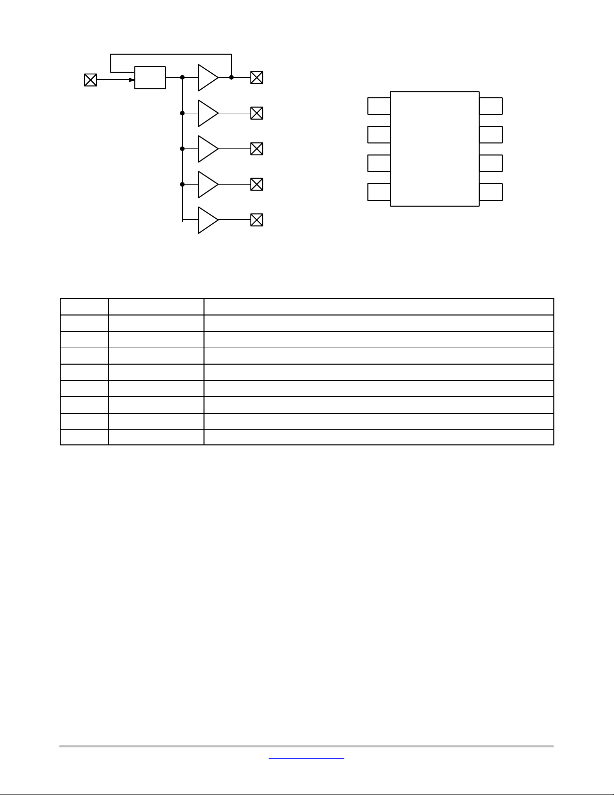
NB2305A
REF
PLL
CLKOUT
CLK1
CLK2
CLK3
CLK4
REF
CLK2
CLK1
GND
Figure 1. Block Diagram
Table 1. PIN DESCRIPTION
Pin # Pin Name Description
1 REF (Note1) Input reference frequency, 5 V tolerant input.
2 CLK2 (Note 2) Buffered clock output.
3 CLK1 (Note 2) Buffered clock output.
4 GND Ground.
5 CLK3 (Note 2) Buffered clock output.
6 V
DD
3.3 V supply.
7 CLK4 (Note 2) Buffered clock output.
8 CLKOUT (Note 2) Buffered clock output, internal feedback on this pin.
1. Weak pulldown.
2. Weak pulldown on all outputs.
1
2
NB2305A
3
4
Figure 2. Pin Configuration
8
7
6
5
CLKOUT
CLK4
V
DD
CLK3
www.onsemi.com
2
Page 3
NB2305A
Table 2. MAXIMUM RATINGS
Parameter Min Max Unit
Supply Voltage to Ground Potential −0.5 +7.0 V
DC Input Voltage (Except REF) −0.5 VDD + 0.5 V
DC Input Voltage (REF) −0.5 7.0 V
Storage Temperature −65 +150 °C
Maximum Soldering Temperature (10 sec) 260 °C
Junction Temperature 150 °C
Static Discharge Voltage (per MIL−STD−883, Method 3015) >2000 V
Stresses exceeding those listed in the Maximum Ratings table may damage the device. If any of these limits are exceeded, device functionality
should not be assumed, damage may occur and reliability may be affected.
Table 3. RECOMMENDED OPERATING CONDITIONS FOR INDUSTRIAL TEMPERATURE DEVICES
Parameter Description Min Max Unit
V
DD
T
A
C
L
C
L
C
IN
Functional operation above the stresses listed in the Recommended Operating Ranges is not implied. Extended exposure to stresses beyond
the Recommended Operating Ranges limits may affect device reliability.
Supply Voltage 3.0 3.6 V
Operating Temperature (Ambient Temperature) Industrial
Commercial
−40
0
85
70
°C
Load Capacitance, below 100 MHz 30 pF
Load Capacitance, from 100 MHz to 133 MHz 10 pF
Input Capacitance 7 pF
Table 4. ELECTRICAL CHARACTERISTICS V
Parameter
V
IL
V
IH
I
IL
I
IH
V
OL
V
OH
I
DD
I
DD
Input LOW Voltage (Note 3) 0.8 V
Input HIGH Voltage (Note 3) 2.0 V
Input LOW Current VIN = 0 V 50
Input HIGH Current VIN = V
Output LOW Voltage IOL = 8 mA (−1)
Output HIGH Voltage IOH = −8 mA (−1)
Supply Current (Commercial Temp) Unloaded outputs at 66.67 MHz,
Supply Current (Industrial Temp) Unloaded outputs at 100 MHz
Description Test Conditions Min Max Unit
= 3.0 V to 3.6 V, GND = 0 V, TA = −40°C to +85°C
CC
DD
I
= 12 mA (−1H)
OL
I
= −12 mA (−1H)
OH
Select inputs at V
DD
66.67 MHz
33 MHz
Select inputs at V
Temp
or GND, at Room
DD
A
100
A
0.4 V
2.4 V
34 mA
50
mA
34
19
Product parametric performance is indicated in the Electrical Characteristics for the listed test conditions, unless otherwise noted. Product
performance may not be indicated by the Electrical Characteristics if operated under different conditions.
3. REF input has a threshold voltage of V
DD
/2.
www.onsemi.com
3
Page 4
NB2305A
Table 5. SWITCHING CHARACTERISTICS V
Parameter
1/t
1/t
t
3
t
4
t
5
t
6
t
7
t
J
t
LOCK
1
1
Output Frequency 30 pF load
Duty Cycle = (t
Output Rise Time (−1)
Output Fall Time (−1)
Output−to−Output Skew All outputs equally loaded 250 ps
Delay, REF Rising Edge to CLKOUT
Rising Edge
Device−to−Device Skew Measured at VDD/2 on the CLKOUT pins of
Cycle−to−Cycle Jitter Measured at 66.67 MHz, loaded outputs 200 ps
PLL Lock Time Stable power supply, valid clock presented
4. All parameters specified with loaded outputs.
Description Test Conditions Min Typ Max Unit
/ t1) * 100 (−1, −1H)
2
(−1H)
(−1H)
(−1H)
= 3.0 V to 3.6 V, GND = 0 V, TA = −40°C to +85°C (Note 4)
CC
15
10 pF load
Measured at 1.4 V, F
= 66.67 MHz
OUT
< 50 MHz
15
40
45
50
50
Measured between 0.8 V and 2.0 V 2.5
Measured between 2.0 V and 0.8 V 2.5
Measured at VDD/2 0 ±350 ps
0 700 ps
the device
on REF pin
100
MHz
133
60
55
1.5
1.5
1.0 ms
%
ns
ns
www.onsemi.com
4
Page 5

NB2305A
Zero Delay and Skew Control
All outputs should be uniformly loaded to achieve Zero
Delay between input and output. Since the CLKOUT pin is
the internal feedback to the PLL, its relative loading can
adjust the input−output delay .
SWITCHING WAVEFORMS
t
1
t
2
1.4 V 1.4 V 1.4 V
Figure 3. Duty Cycle Timing
OUTPUT
OUTPUT
1.4 V
t
5
1.4 V
For applications requiring zero input−output delay, all
outputs, including CLKOUT, must be equally loaded. Even
if CLKOUT is not used, it must have a capacitive load equal
to that on other outputs, for obtaining zero−input−output
delay.
2.0 V
V
DD
2
0.8 V
t
4
OUTPUT
2.0 V
0.8 V
t
3
Figure 4. All Outputs Rise/Fall Time
V
DD
INPUT
OUTPUT
2
t
6
3.3 V
0 V
Figure 5. Output − Output Skew
CLKOUT, Device 1
CLKOUT, Device 2
t
7
Figure 6. Input − Output Propagation Delay
V
DD
2
V
DD
2
Figure 7. Device − Device Skew
www.onsemi.com
5
Page 6

NB2305A
8
V
TEST CIRCUITS
DD
V
DD
0.1 F
0.1 F
OUTPUTS
V
DD
GND GND
Figure 8. Test Circuit #1
CLKOUT
C
LOAD
V
DD
0.1 F
V
DD
0.1 F
GND GND
Figure 9. Test Circuit #2
For parameter t
OUTPUTS
(output slew rate) on −1H devices
1 k
1 k
10 pF
ORDERING INFORMATION
Device Marking Operating Range Package Shipping
NB2305AI1DG 5I1 Industrial &
Commercial
NB2305AI1DR2G 5I1 Industrial &
Commercial
NB2305AI1HDG 5I1H Industrial &
Commercial
NB2305AI1HDR2G 5I1H Industrial &
Commercial
NB2305AI1DTG 5I1 Industrial &
Commercial
NB2305AI1DTR2G 5I1 Industrial &
Commercial
NB2305AI1HDTG 5IH Industrial &
Commercial
NB2305AI1HDTR2G 5IH Industrial &
Commercial
SOIC−8
(Pb−Free)
SOIC−8
(Pb−Free)
SOIC−8
(Pb−Free)
SOIC−8
(Pb−Free)
TSSOP−8
(Pb−Free)
TSSOP−8
(Pb−Free)
TSSOP−8
(Pb−Free)
TSSOP−8
(Pb−Free)
98 Units / Rail
2500 Tape & Reel
98 Units / Rail
2500 Tape & Reel
100 Units / Rail
2500 Tape & Reel
100 Units / Rail
2500 Tape & Reel
†For information on tape and reel specifications, including part orientation and tape sizes, please refer to our Tape and Reel Packaging
Specifications Brochure, BRD8011/D.
†
Availability
Now
Now
Now
Now
Now
Now
Now
Now
Pentium is a registered trademark of Intel Corporation.
www.onsemi.com
6
Page 7

MECHANICAL CASE OUTLINE
PACKAGE DIMENSIONS
8
1
SCALE 1:1
B
−Y−
−Z−
−X−
A
58
1
4
G
H
D
0.25 (0.010) Z
M
SOLDERING FOOTPRINT*
7.0
0.275
S
Y
0.25 (0.010)
C
SXS
SEATING
PLANE
0.10 (0.004)
1.52
0.060
4.0
0.155
CASE 751−07
M
M
Y
N
SOIC−8 NB
ISSUE AK
K
X 45
_
M
J
MARKING DIAGRAM*
8
XXXXX
ALYWX
1
XXXXX = Specific Device Code
A = Assembly Location
L = Wafer Lot
Y = Year
W = Work Week
G = Pb−Free Package
8
XXXXX
ALYWX
G
1
IC
IC
(Pb−Free)
DATE 16 FEB 2011
NOTES:
1. DIMENSIONING AND TOLERANCING PER
ANSI Y14.5M, 1982.
2. CONTROLLING DIMENSION: MILLIMETER.
3. DIMENSION A AND B DO NOT INCLUDE
MOLD PROTRUSION.
4. MAXIMUM MOLD PROTRUSION 0.15 (0.006)
PER SIDE.
5. DIMENSION D DOES NOT INCLUDE DAMBAR
PROTRUSION. ALLOWABLE DAMBAR
PROTRUSION SHALL BE 0.127 (0.005) TOTAL
IN EXCESS OF THE D DIMENSION AT
MAXIMUM MATERIAL CONDITION.
6. 751−01 THRU 751−06 ARE OBSOLETE. NEW
STANDARD IS 751−07.
MILLIMETERS
DIMAMIN MAX MIN MAX
4.80 5.00 0.189 0.197
B 3.80 4.00 0.150 0.157
C 1.35 1.75 0.053 0.069
D 0.33 0.51 0.013 0.020
G 1.27 BSC 0.050 BSC
H 0.10 0.25 0.004 0.010
J 0.19 0.25 0.007 0.010
K 0.40 1.27 0.016 0.050
M 0 8 0 8
____
N 0.25 0.50 0.010 0.020
S 5.80 6.20 0.228 0.244
INCHES
GENERIC
8
XXXXXX
AYWW
1
Discrete
XXXXXX = Specific Device Code
A = Assembly Location
Y = Year
WW = Work Week
G = Pb−Free Package
8
XXXXXX
AYWW
1
Discrete
(Pb−Free)
G
0.6
0.024
1.270
0.050
SCALE 6:1
ǒ
inches
mm
Ǔ
*This information is generic. Please refer to
device data sheet for actual part marking.
Pb−Free indicator, “G” or microdot “G”, may
or may not be present. Some products may
not follow the Generic Marking.
*For additional information on our Pb−Free strategy and soldering
details, please download the ON Semiconductor Soldering and
Mounting Techniques Reference Manual, SOLDERRM/D.
STYLES ON PAGE 2
DOCUMENT NUMBER:
DESCRIPTION:
ON Semiconductor and are trademarks of Semiconductor Components Industries, LLC dba ON Semiconductor or its subsidiaries in the United States and/or other countries.
ON Semiconductor reserves the right to make changes without further notice to any products herein. ON Semiconductor makes no warranty, representation or guarantee regarding
the suitability of its products for any particular purpose, nor does ON Semiconductor assume any liability arising out of the application or use of any product or circuit, and specifically
disclaims any and all liability, including without limitation special, consequential or incidental damages. ON Semiconductor does not convey any license under its patent rights nor the
rights of others.
© Semiconductor Components Industries, LLC, 2019
98ASB42564B
SOIC−8 NB
Electronic versions are uncontrolled except when accessed directly from the Document Repository.
Printed versions are uncontrolled except when stamped “CONTROLLED COPY” in red.
PAGE 1 OF 2
www.onsemi.com
Page 8

STYLE 1:
PIN 1. EMITTER
2. COLLECTOR
3. COLLECTOR
4. EMITTER
5. EMITTER
6. BASE
7. BASE
8. EMITTER
STYLE 5:
PIN 1. DRAIN
2. DRAIN
3. DRAIN
4. DRAIN
5. GATE
6. GATE
7. SOURCE
8. SOURCE
STYLE 9:
PIN 1. EMITTER, COMMON
2. COLLECTOR, DIE #1
3. COLLECTOR, DIE #2
4. EMITTER, COMMON
5. EMITTER, COMMON
6. BASE, DIE #2
7. BASE, DIE #1
8. EMITTER, COMMON
STYLE 13:
PIN 1. N.C.
2. SOURCE
3. SOURCE
4. GATE
5. DRAIN
6. DRAIN
7. DRAIN
8. DRAIN
STYLE 17:
PIN 1. VCC
2. V2OUT
3. V1OUT
4. TXE
5. RXE
6. VEE
7. GND
8. ACC
STYLE 21:
PIN 1. CATHODE 1
2. CATHODE 2
3. CATHODE 3
4. CATHODE 4
5. CATHODE 5
6. COMMON ANODE
7. COMMON ANODE
8. CATHODE 6
STYLE 25:
PIN 1. VIN
2. N/C
3. REXT
4. GND
5. IOUT
6. IOUT
7. IOUT
8. IOUT
STYLE 29:
PIN 1. BASE, DIE #1
2. EMITTER, #1
3. BASE, #2
4. EMITTER, #2
5. COLLECTOR, #2
6. COLLECTOR, #2
7. COLLECTOR, #1
8. COLLECTOR, #1
STYLE 2:
PIN 1. COLLECTOR, DIE, #1
2. COLLECTOR, #1
3. COLLECTOR, #2
4. COLLECTOR, #2
5. BASE, #2
6. EMITTER, #2
7. BASE, #1
8. EMITTER, #1
STYLE 6:
PIN 1. SOURCE
2. DRAIN
3. DRAIN
4. SOURCE
5. SOURCE
6. GATE
7. GATE
8. SOURCE
STYLE 10:
PIN 1. GROUND
2. BIAS 1
3. OUTPUT
4. GROUND
5. GROUND
6. BIAS 2
7. INPUT
8. GROUND
STYLE 14:
PIN 1. N−SOURCE
2. N−GATE
3. P−SOURCE
4. P−GATE
5. P−DRAIN
6. P−DRAIN
7. N−DRAIN
8. N−DRAIN
STYLE 18:
PIN 1. ANODE
2. ANODE
3. SOURCE
4. GATE
5. DRAIN
6. DRAIN
7. CATHODE
8. CATHODE
STYLE 22:
PIN 1. I/O LINE 1
2. COMMON CATHODE/VCC
3. COMMON CATHODE/VCC
4. I/O LINE 3
5. COMMON ANODE/GND
6. I/O LINE 4
7. I/O LINE 5
8. COMMON ANODE/GND
STYLE 26:
PIN 1. GND
2. dv/dt
3. ENABLE
4. ILIMIT
5. SOURCE
6. SOURCE
7. SOURCE
8. VCC
STYLE 30:
PIN 1. DRAIN 1
2. DRAIN 1
3. GATE 2
4. SOURCE 2
5. SOURCE 1/DRAIN 2
6. SOURCE 1/DRAIN 2
7. SOURCE 1/DRAIN 2
8. GATE 1
SOIC−8 NB
CASE 751−07
ISSUE AK
STYLE 3:
STYLE 7:
STYLE 11:
STYLE 15:
STYLE 19:
STYLE 23:
PIN 1. DRAIN, DIE #1
2. DRAIN, #1
3. DRAIN, #2
4. DRAIN, #2
5. GATE, #2
6. SOURCE, #2
7. GATE, #1
8. SOURCE, #1
PIN 1. INPUT
2. EXTERNAL BYPASS
3. THIRD STAGE SOURCE
4. GROUND
5. DRAIN
6. GATE 3
7. SECOND STAGE Vd
8. FIRST STAGE Vd
PIN 1. SOURCE 1
2. GATE 1
3. SOURCE 2
4. GATE 2
5. DRAIN 2
6. DRAIN 2
7. DRAIN 1
8. DRAIN 1
PIN 1. ANODE 1
2. ANODE 1
3. ANODE 1
4. ANODE 1
5. CATHODE, COMMON
6. CATHODE, COMMON
7. CATHODE, COMMON
8. CATHODE, COMMON
PIN 1. SOURCE 1
2. GATE 1
3. SOURCE 2
4. GATE 2
5. DRAIN 2
6. MIRROR 2
7. DRAIN 1
8. MIRROR 1
PIN 1. LINE 1 IN
2. COMMON ANODE/GND
3. COMMON ANODE/GND
4. LINE 2 IN
5. LINE 2 OUT
6. COMMON ANODE/GND
7. COMMON ANODE/GND
8. LINE 1 OUT
STYLE 27:
PIN 1. ILIMIT
2. OVLO
3. UVLO
4. INPUT+
5. SOURCE
6. SOURCE
7. SOURCE
8. DRAIN
DATE 16 FEB 2011
STYLE 4:
PIN 1. ANODE
2. ANODE
3. ANODE
4. ANODE
5. ANODE
6. ANODE
7. ANODE
8. COMMON CATHODE
STYLE 8:
PIN 1. COLLECTOR, DIE #1
2. BASE, #1
3. BASE, #2
4. COLLECTOR, #2
5. COLLECTOR, #2
6. EMITTER, #2
7. EMITTER, #1
8. COLLECTOR, #1
STYLE 12:
PIN 1. SOURCE
2. SOURCE
3. SOURCE
4. GATE
5. DRAIN
6. DRAIN
7. DRAIN
8. DRAIN
STYLE 16:
PIN 1. EMITTER, DIE #1
2. BASE, DIE #1
3. EMITTER, DIE #2
4. BASE, DIE #2
5. COLLECTOR, DIE #2
6. COLLECTOR, DIE #2
7. COLLECTOR, DIE #1
8. COLLECTOR, DIE #1
STYLE 20:
PIN 1. SOURCE (N)
2. GATE (N)
3. SOURCE (P)
4. GATE (P)
5. DRAIN
6. DRAIN
7. DRAIN
8. DRAIN
STYLE 24:
PIN 1. BASE
2. EMITTER
3. COLLECTOR/ANODE
4. COLLECTOR/ANODE
5. CATHODE
6. CATHODE
7. COLLECTOR/ANODE
8. COLLECTOR/ANODE
STYLE 28:
PIN 1. SW_TO_GND
2. DASIC_OFF
3. DASIC_SW_DET
4. GND
5. V_MON
6. VBULK
7. VBULK
8. VIN
DOCUMENT NUMBER:
DESCRIPTION:
ON Semiconductor and are trademarks of Semiconductor Components Industries, LLC dba ON Semiconductor or its subsidiaries in the United States and/or other countries.
ON Semiconductor reserves the right to make changes without further notice to any products herein. ON Semiconductor makes no warranty, representation or guarantee regarding
the suitability of its products for any particular purpose, nor does ON Semiconductor assume any liability arising out of the application or use of any product or circuit, and specifically
disclaims any and all liability, including without limitation special, consequential or incidental damages. ON Semiconductor does not convey any license under its patent rights nor the
rights of others.
© Semiconductor Components Industries, LLC, 2019
98ASB42564B
SOIC−8 NB
Electronic versions are uncontrolled except when accessed directly from the Document Repository.
Printed versions are uncontrolled except when stamped “CONTROLLED COPY” in red.
PAGE 2 OF 2
www.onsemi.com
Page 9

MECHANICAL CASE OUTLINE
PACKAGE DIMENSIONS
SCALE 2:1
TSSOP−8
CASE 948S−01
ISSUE C
DATE 20 JUN 2008
0.076 (0.003)
−T−
SEATING
PLANE
8x REFK
U
T
JJ1
S
S
K1
K
SECTION N−N
S
U0.20 (0.008) T
2X L/2
85
L
PIN 1
IDENT
S
U0.20 (0.008) T
0.10 (0.004) V
−U−
1
4
A
M
B
−V−
C
D
G
DETAIL E
N
0.25 (0.010)
M
−W−
NOTES:
1. DIMENSIONING AND TOLERANCING PER ANSI
Y14.5M, 1982.
2. CONTROLLING DIMENSION: MILLIMETER.
3. DIMENSION A DOES NOT INCLUDE MOLD FLASH.
PROTRUSIONS OR GATE BURRS. MOLD FLASH
OR GATE BURRS SHALL NOT EXCEED 0.15
(0.006) PER SIDE.
4. DIMENSION B DOES NOT INCLUDE INTERLEAD
FLASH OR PROTRUSION. INTERLEAD FLASH OR
PROTRUSION SHALL NOT EXCEED 0.25 (0.010)
PER SIDE.
5. TERMINAL NUMBERS ARE SHOWN FOR
REFERENCE ONLY.
6. DIMENSION A AND B ARE TO BE DETERMINED
AT DATUM PLANE -W-.
DIM MIN MAX MIN MAX
A 2.90 3.10 0.114 0.122
B 4.30 4.50 0.169 0.177
C --- 1.10 --- 0.043
D 0.05 0.15 0.002 0.006
F 0.50 0.70 0.020 0.028
G 0.65 BSC 0.026 BSC
J 0.09 0.20 0.004 0.008
J1 0.09 0.16 0.004 0.006
K 0.19 0.30 0.007 0.012
K1 0.19 0.25 0.007 0.010
L 6.40 BSC 0.252 BSC
M 0 8 0 8
____
INCHESMILLIMETERS
N
GENERIC
F
DETAIL E
MARKING DIAGRAM*
XXX
YWW
A G
G
XXX = Specific Device Code
A = Assembly Location
Y = Year
WW = Work Week
G = Pb−Free Package
DOCUMENT NUMBER:
STATUS:
NEW STANDARD:
© Semiconductor Components Industries, LLC, 2002
October, 2002 − Rev. 0
DESCRIPTION:
98AON00697D
ON SEMICONDUCTOR STANDARD
TSSOP−8
http://onsemi.com
1
*This information is generic. Please refer to
device data sheet for actual part marking.
Pb−Free indicator, “G” or microdot “ G”,
may or may not be present.
Electronic versions are uncontrolled except when
accessed directly from the Document Repository. Printed
versions are uncontrolled except when stamped
“CONTROLLED COPY” in red.
Case Outline Number:
PAGE 1 OF 2
XXX
Page 10

DOCUMENT NUMBER:
98AON00697D
PAGE 2 OF 2
ISSUE REVISION DATE
O RELEASED FOR PRODUCTION. 18 APR 2000
A ADDED MARKING DIAGRAM INFORMATION. REQ. BY V. BASS. 13 JAN 2006
B CORRECTED MARKING DIAGRAM PIN 1 LOCATION AND MARKING. REQ. BY C.
13 MAR 2006
REBELLO.
C REMOVED EXPOSED PAD VIEW AND DIMENSIONS P AND P1. CORRECTED
20 JUN 2008
MARKING INFORMATION. REQ. BY C. REBELLO.
ON Semiconductor and are registered trademarks of Semiconductor Components Industries, LLC (SCILLC). SCILLC reserves the right to make changes without further notice
to any products herein. SCILLC makes no warranty, representation or guarantee regarding the suitability of its products for any particular purpose, nor does SCILLC assume any liability
arising out of the application or use of any product or circuit, and specifically disclaims any and all liability, including without limitation special, consequential or incidental damages.
“Typical” parameters which may be provided in SCILLC data sheets and/or specifications can and do vary in different applications and actual performance may vary over time. All
operating parameters, including “Typicals” must be validated for each customer application by customer’s technical experts. SCILLC does not convey any license under its patent rights
nor the rights of others. SCILLC products are not designed, intended, or authorized for use as components in systems intended for surgical implant into the body, or other applications
intended to support or sustain life, or for any other application in which the failure of the SCILLC product could create a situation where personal injury or death may occur. Should
Buyer purchase or use SCILLC products for any such unintended or unauthorized application, Buyer shall indemnify and hold SCILLC and its officers, employees, subsidiaries, affiliates,
and distributors harmless against all claims, costs, damages, and expenses, and reasonable attorney fees arising out of, directly or indirectly, any claim of personal injury or death
associated with such unintended or unauthorized use, even if such claim alleges that SCILLC was negligent regarding the design or manufacture of the part. SCILLC is an Equal
Opportunity/Affirmative Action Employer. This literature is subject to all applicable copyright laws and is not for resale in any manner.
© Semiconductor Components Industries, LLC, 2008
Case Outline Number:
June, 2008 − Rev. 01C
948S
Page 11

ON Semiconductor and are trademarks of Semiconductor Components Industries, LLC dba ON Semiconductor or its subsidiaries in the United States and/or other countries.
ON Semiconductor owns the rights to a number of patents, trademarks, copyrights, trade secrets, and other intellectual property. A listing of ON Semiconductor’s product/patent
coverage may be accessed at www.onsemi.com/site/pdf/Patent−Marking.pdf
ON Semiconductor makes no warranty, representation or guarantee regarding the suitability of its products for any particular purpose, nor does ON Semiconductor assume any liability
arising out of the application or use of any product or circuit, and specifically disclaims any and all liability, including without limitation special, consequential or incidental damages.
Buyer is responsible for its products and applications using ON Semiconductor products, including compliance with all laws, regulations and safety requirements or standards,
regardless of any support or applications information provided by ON Semiconductor. “Typical” parameters which may be provided in ON Semiconductor data sheets and/or
specifications can and do vary in different applications and actual performance may vary over time. All operating parameters, including “Typicals” must be validated for each customer
application by customer’s technical experts. ON Semiconductor does not convey any license under its patent rights nor the rights of others. ON Semiconductor products are not
designed, intended, or authorized for use as a critical component in life support systems or any FDA Class 3 medical devices or medical devices with a same or similar classification
in a foreign jurisdiction or any devices intended for implantation in the human body. Should Buyer purchase or use ON Semiconductor products for any such unintended or unauthorized
application, Buyer shall indemnify and hold ON Semiconductor and its officers, employees, subsidiaries, affiliates, and distributors harmless against all claims, costs, damages, and
expenses, and reasonable attorney fees arising out of, directly or indirectly, any claim of personal injury or death associated with such unintended or unauthorized use, even if such
claim alleges that ON Semiconductor was negligent regarding the design or manufacture of the part. ON Semiconductor is an Equal Opportunity/Affirmative Action Employer. This
literature is subject to all applicable copyright laws and is not for resale in any manner.
. ON Semiconductor reserves the right to make changes without further notice to any products herein.
PUBLICATION ORDERING INFORMATION
LITERATURE FULFILLMENT:
Email Requests to: orderlit@onsemi.com
ON Semiconductor Website: www.onsemi.com
TECHNICAL SUPPORT
North American Technical Support:
Voice Mail: 1 800−282−9855 Toll Free USA/Canada
Phone: 011 421 33 790 2910
Europe, Middle East and Africa Technical Support:
Phone: 00421 33 790 2910
For additional information, please contact your local Sales Representative
◊
www.onsemi.com
1
 Loading...