

Page 1
N25S818HA
256 kb Low Power Serial
SRAMs
32 k x 8 Bit Organization
Introduction
The ON Semiconductor serial SRAM family includes several
integrated memory devices including this 256 kb serially accessed
Static Random Access Memory, internally organized as 32 k words by
8 bits. The devices are designed and fabricated using
ON Semiconductor’s advanced CMOS technology to provide both
high−speed performance and low power. The devices operate with a
single chip select (CS
Interface (SPI) serial bus. A single data in and data out line is used
along with a clock to access data within the devices. The N25S818HA
devices include a HOLD
to be paused. While paused, input transitions will be ignored. The
devices can operate over a wide temperature range of −40°C to +85°C
and can be available in several standard package offerings.
Features
• Power Supply Range: 1.7 to 1.95 V
• Very Low Standby Current: Typical Isb as low as 200 nA
• Very Low Operating Current: As low as 3 mA
• Simple Memory Control:
Single chip select (CS
Serial input (SI) and serial output (SO)
• Flexible Operating Modes:
Word read and write
Page mode (32 word page)
Burst mode (full array)
• Organization: 32 k x 8 bit
• Self Timed Write Cycles
• Built−in Write Protection (CS High)
• HOLD Pin for Pausing Communication
• High Reliability: Unlimited write cycles
• Green SOIC and TSSOP
• These Devices are Pb−Free, Halogen Free/BFR Free and are RoHS
Compliant
) input and use a simple Serial Peripheral
pin that allows communication to the device
)
http://onsemi.com
MARKING
DIAGRAMS
C124
TSSOP−8
T SUFFIX
CASE 948AL
SOIC−8
S SUFFIX
CASE 751BD
XXXX = Date Code
Y = Assembly Code
ZZ = Lot Traceability
ORDERING INFORMATION
Device Package
N25S818HAS21I SOIC−8
(Pb−Free)
N25S818HAT21I TSSOP−8
(Pb−Free)
N25S818HAS21IT SOIC−8
(Pb−Free)
N25S818HAT21IT TSSOP−8
(Pb−Free)
†For information on tape and reel specifications,
including part orientation and tape sizes, please
refer to our Tape and Reel Packaging Specification
Brochure, BRD8011/D.
XXXXYZZ
C114
XXXXYZZ
Shipping
100 Units / Tube
100 Units / Tube
3000 / Tape &
Reel
3000 / Tape &
Reel
†
© Semiconductor Components Industries, LLC, 2012
June, 2012 − Rev. 12
1 Publication Order Number:
N25S818HA/D
Page 2
N25S818HA
1
CS
SO
NC
VSS
TSSOP−8
VCC
HOLD
SCK
SI
Figure 1. Pin Connections
(Top View)
Table 1. DEVICE OPTIONS
Power
Part Number Density
N25S818HAS2
N25S818HAT2 TSSOP
256 Kb 1.8 16
Supply (V)
Speed
(MHz)
Package
SOIC
Table 2. PIN NAMES
Pin Name Pin Function
CS Chip Select Input
SCK Serial Clock Input
SI Serial Data Input
SO Serial Data Output
HOLD Hold Input
NC No Connect
V
CC
V
SS
Power
Ground
CS
SO
NC
VSS
1
VCC
HOLD
SCK
SI
SOIC−8
Typical Standby
Current
200 nA 3 mA @ 1 Mhz
Read/Write
Operating Current
SCK
HOLD
CS
SO
Clock
Circuitry
Decode
Logic
SI
Data In
Receiver
Data Out
Buffer
SRAM
Array
Figure 2. Functional Block Diagram
http://onsemi.com
2
Page 3
N25S818HA
Table 3. ABSOLUTE MAXIMUM RATINGS
Item Symbol Rating Unit
Voltage on any pin relative to V
Voltage on VCC Supply Relative to V
SS
SS
Power Dissipation P
Storage Temperature T
Operating Temperature T
Soldering Temperature and Time T
Stresses exceeding Maximum Ratings may damage the device. Maximum Ratings are stress ratings only. Functional operation above the
Recommended Operating Conditions is not implied. Extended exposure to stresses above the Recommended Operating Conditions may affect
device reliability.
Table 4. OPERATING CHARACTERISTICS (Over Specified Temperature Range)
Item Symbol Test Conditions Min
Supply Voltage V
Input High Voltage V
Input Low Voltage V
Output High Voltage V
Output Low Voltage V
Input Leakage Current I
Output Leakage Current I
Read/Write Operating Current
Standby Current I
I
I
I
CC
IH
IL
OH
OL
LI
LO
CC1
CC2
CC3
SB
1. Typical values are measured at Vcc = Vcc Typ., TA = 25°C and are not 100% tested.
1.8 V Device 1.7 1.95 V
IOH = −0.4 mA VCC – 0.5 V
IOL = 1 mA 0.2 V
CS = VCC, VIN = 0 to V
CS = VCC, V
F = 1 MHz, I
F = 10 MHz, I
F = fCLK MAX, I
CS = VCC, VIN = VSS or V
V
IN,OUT
V
CC
D
STG
A
SOLDER
–0.3 to VCC + 0.3 V
–0.3 to 4.5 V
500 mW
–40 to 125 °C
−40 to +85 °C
260°C, 10 sec °C
Typ
(Note 1)
0.7 x V
CC
VCC + 0.3 V
−0.3 0.8 V
CC
= 0 to V
OUT
OUT
CC
= 0 3 mA
= 0 6 mA
OUT
= 0 10 mA
OUT
CC
200 500 nA
Max Unit
0.5
0.5
mA
mA
Table 5. CAPACITANCE (Note 2)
Item
Input Capacitance C
I/O Capacitance C
2. These parameters are verified in device characterization and are not 100% tested
Symbol Test Condition Min Max Unit
IN
I/O
VIN = 0 V, f = 1 MHz, TA = 25°C 7 pF
VIN = 0 V, f = 1 MHz, TA = 25°C 7 pF
http://onsemi.com
3
Page 4
N25S818HA
Table 6. TIMING TEST CONDITIONS
Item
Input Pulse Level 0.1 VCC to 0.9 V
Input Rise and Fall Time 5 ns
Input and Output Timing Reference Levels 0.5 V
Output Load CL = 100 pF
Operating Temperature −40 to +85°C
Table 7. TIMING
Item Symbol Min Max Units
Clock Frequency f
Clock Rise Time t
Clock Fall Time t
Clock High Time t
Clock Low Time t
Clock Delay Time t
CS Setup Time t
CS Hold Time t
CS Disable Time t
SCK to CS t
Data Setup Time t
Data Hold Time t
Output Valid From Clock Low t
Output Hold Time t
Output Disable Time t
HOLD Setup Time t
HOLD Hold Time t
HOLD Low to Output High−Z t
HOLD High to Output Valid t
CLK
R
F
HI
LO
CLD
CSS
CSH
CSD
SCS
SU
HD
V
HO
DIS
HS
HH
HZ
HV
CC
32 ns
32 ns
32 ns
32 ns
50 ns
32 ns
5 ns
10 ns
10 ns
0 ns
10 ns
10 ns
10 ns
CC
16 MHz
2
2
32 ns
20 ns
50 ns
ms
ms
http://onsemi.com
4
Page 5
N25S818HA
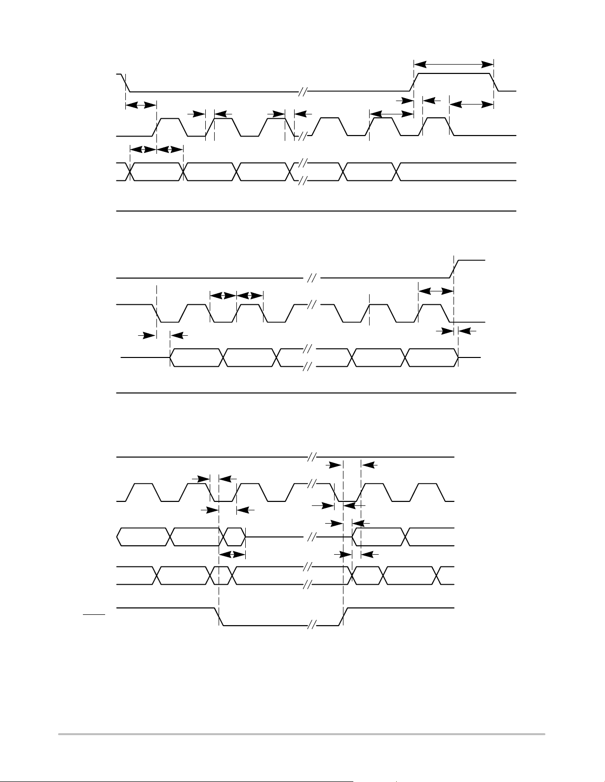
t
CSD
CS
SCK
SO
CS
SCK
SO
t
CLD
t
R
t
CSS
t
SU
SI
MSB in
t
HD
t
F
t
CSH
t
SCS
LSB in
High−Z
Figure 3. Serial Input Timing
t
t
V
MSB out
LOtHI
t
CSH
LSB out
t
DIS
SI
CS
SCK
SO n+1 n
SI
n+2
t
HZ
n+2 n+1 n
HOLD
Don’t Care
Figure 4. Serial Output Timing
t
HS
t
HH
High−Z
Don’t Care
Figure 5. Hold Timing
t
HH
t
HS
t
HV
nn−1
t
SU
nn−1
http://onsemi.com
5
Page 6

N25S818HA
Table 8. CONTROL SIGNAL DESCRIPTIONS
Signal Name I/O Description
CS Chip Select I A low level selects the device and a high level puts the device in standby mode. If CS is brought
SCK Serial Clock I Synchronizes all activities between the memory and controller. All incoming addresses, data and
SI Serial Data In I Receives instructions, addresses and data on the rising edge of SCK.
SO Serial Data Out O Data is transferred out after the falling edge of SCK.
HOLD Hold I A high level is required for normal operation. Once the device is selected and a serial sequence is
Functional Operation
Basic Operation
The 256 Kb serial SRAM is designed to interface directly
with a standard Serial Peripheral Interface (SPI) common on
many standard micro−controllers. It may also interface with
other non−SPI ports by programming discrete I/O lines to
operate the device.
The serial SRAM contains an 8−bit instruction register
and is accessed via the SI pin. The CS
the HOLD
pin must be high for the entire operation. Data is
high during a program cycle, the cycle will complete and then the device will enter standby mode.
When CS
being started.
instructions are latched on the rising edge of SCK. Data out is updated on SO after the falling edge
of SCK.
started, this input may be taken low to pause serial communication without resetting the serial sequence. The pin must be brought low while SCK is low for immediate use. If SCK is not low, the
Hold function will not be invoked until the next SCK high to low transition. The device must remain
selected during this sequence. SO is high−Z during the Hold time and SI and SCK are inputs are
ignored. To resume operations, HOLD
Lowering the HOLD
is high, SO is in high−Z. CS must be driven low after power−up prior to any sequence
must be pulled high while the SCK pin is low.
input at any time will take to SO output to High−Z.
sampled on the first rising edge of SCK after CS
If the clock line is shared, the user can assert the HOLD
and place the device into a Hold mode. After releasing the
HOLD
pin, the operation will resume from the point where
it was held.
The following table contains the possible instructions and
pin must be low and
formats. All instructions, addresses and data are transferred
MSB first and LSB last.
goes low.
input
Table 9. INSTRUCTION SET
Instruction Instruction Format Description
READ 0000 0011 Read data from memory starting at selected address
WRITE 0000 0010 Write data to memory starting at selected address
RDSR 0000 0101 Read status register
WRSR 0000 0001 Write status register
READ Operations
The serial SRAM READ is selected by enabling CS low.
First, the 8−bit READ instruction is transmitted to the device
followed by the 16−bit address with the MSB being a don’t
care. After the READ instruction and addresses are sent, the
data stored at that address in memory is shifted out on the SO
pin after the output valid time from the clock edge.
If operating in page mode, after the initial word of data is
shifted out, the data stored at the next memory location on
the page can be read sequentially by continuing to provide
clock pulses. The internal address pointer is automatically
incremented to the next higher address on the page after each
word of data is read out. This can be continued for the entire
page length of 32 words long. At the end of the page, the
addresses pointer will be wrapped to the 0 word address
within the page and the operation can be continuously
looped over the 32 words of the same page.
If operating in burst mode, after the initial word of data is
shifted out, the data stored at the next memory location can
be read sequentially by continuing to provide clock pulses.
The internal address pointer is automatically incremented to
the next higher address after each word of data is read out.
This can be continued for the entire array and when the
highest address is reached (7FFFh), the address counter
wraps to the address 0000h. This allows the burst read cycle
to be continued indefinitely.
All READ operations are terminated by pulling CS
high.
http://onsemi.com
6
Page 7

CS
N25S818HA
SCK
SO
CS
SCK
SO
043251698107 11
Instruction
000 00 011
SI
High−Z
15 14 13 12 210
Figure 6. Word READ Sequence
043251698107 11
Instruction
000 00011
SI
15 14 13 12 210
16−bit address
16−bit address
ADDR 1
21 2322 24 28 29 30 3126 2725
7
6543210
21 2322 24 28 29 30 3126 2725
7
6543210High−Z
Data Out
Don’t Care
Data Out from ADDR 1
32 3433 35 39 40 41 4237 3836 43 4544 46 47
Don’t Care
Data Out from ADDR 2
7 6543210
Data Out from ADDR 3
7 6543210 7 6543210
Figure 7. Page and Burst READ Sequence
Data Out from ADDR n
...
http://onsemi.com
7
Page 8

N25S818HA
SI
16−bit address
Page address (X)
Word address (Y)
SO
Data Words: sequential, at the end of the page the
address wraps back to the beginning of the page
Page X
Word Y
Word Y+1
Figure 8. Page READ Sequence
SI
16−bit address
Page address (X)
Word address (Y)
SO
Page X
Word Y
Data Words: sequential, at the end of the page the address wraps to the beginning
of the page and continues incrementing up to the starting word address. At that
time, the address increments to the next page and the burst continues.
. . .
Page X
Word Y+1
Page X
Word 31
Figure 9. Burst READ Sequence
WRITE Operations
The serial SRAM WRITE is selected by enabling CS low.
First, the 8−bit WRITE instruction is transmitted to the
device followed by the 16−bit address with the MSB being
a don’t care. After the WRITE instruction and addresses are
sent, the data to be stored in memory is shifted in on the SI
pin.
If operating in page mode, after the initial word of data is
shifted in, additional data words can be written as long as the
address requested is sequential on the same page. Simply
write the data on SI pin and continue to provide clock pulses.
The internal address pointer is automatically incremented to
the next higher address on the page after each word of data
is written in. This can be continued for the entire page length
of 32 words long. At the end of the page, the addresses
pointer will be wrapped to the 0 word address within the
Page XPage X
Word Y+2
Page X
Word 31
Page X
Word 0
Page X
Word 1
. . .
Page X
Word 0
Page X
Word 1
Page X
Word Y−1
page and the operation can be continuously looped over the
32 words of the same page. The new data will replace data
already stored in the memory locations.
If operating in burst mode, after the initial word of data is
shifted in, additional data words can be written to the next
sequential memory locations by continuing to provide clock
pulses. The internal address pointer is automatically
incremented to the next higher address after each word of
data is read out. This can be continued for the entire array
and when the highest address is reached (7FFFh), the
address counter wraps to the address 0000h. This allows the
burst write cycle to be continued indefinitely. Again, the new
data will replace data already stored in the memory
locations.
All WRITE operations are terminated by pulling CS
Page X+1
Word Y
Page X+1
Word Y+1
high.
CS
SCK
SO
043251698107 11
Instruction
SI
000 00010
High−Z
15 14 13 12 21076543210
Figure 10. Word WRITE Sequence
21 2322 24 28 29 30 3126 2725
16−bit address Data In
...
http://onsemi.com
8
Page 9

CS
N25S818HA
043251698107 11
SCK
Instruction
000 00010
SI
SO
32 3433 35 39 40 41 4237 3836 43 4544 46 47
Data In to ADDR 2
7 6543210
15 14 13 12 210 76543210
7 6543210 7 6543210
16−bit address
ADDR 1
High−Z
Data In to ADDR 3 Data In to ADDR n
High−Z
Figure 11. Page and Burst WRITE Sequence
21 2322 24 28 29 30 3126 2725
Data In to ADDR 1
...
SI
SO
SI
16−bit address
Page address (X)
Word address (Y)
SO
16−bit address
Page address (X)
Word address (Y)
Page X
Word Y
Data Words: sequential, at the end of the page the address wraps to the beginning of the page and
continues incrementing up to the starting word address. At that time, the address increments to the
next page and the burst continues.
Data Words: sequential, at the end of the page the
address wraps back to the beginning of the page
Page X
Word Y
Page X
Word Y+1
Page X
Word Y+2
High−Z
Page X
Word 31
Figure 12. Page WRITE Sequence
. . .
Page X
Word Y+1
Figure 13. Burst WRITE Sequence
Page X
Word 31
Page X
Word 0
High−Z
Page X
Word 1
. . .
Page X
Word 0
Page X
Word Y−1
Page X
Word 1
Page X+1
Word Y
Page X+1
Word Y+1
http://onsemi.com
9
Page 10

N25S818HA
WRITE Status Register Instruction (WRSR)
This instruction provides the ability to write the status
register and select among several operating modes. Several
of the register bits must be set to a low ‘0’ if any of the other
CS
bits are written. The timing sequence to write to the status
register is shown below, followed by the organization of the
status register.
SCK
SI
SO
Mode
0 0 = Word Mode (Default)
1 0 = Page Mode
0 1 = Burst Mode
1 1 = Reserved
04325169810711
00 000 10
Instruction
0
High−Z
Status Register Data In
7 6543210
Figure 14. WRITE Status Register Sequence
Reserved
Must = 0
Reserved
Must = 0
Figure 15. Status Register
12 13 14 15
Bit 0Bit 1Bit 2Bit 3Bit 4Bit 5Bit 6Bit 7
Hold Function
0 = Hold (Default)
1 = No Hold
READ Status Register Instruction (RDSR)
This instruction provides the ability to read the Status register. The register may be read at any time by performing the
following timing sequence.
CS
SCK
SI
SO
04325169810711
Instruction
00 000 10
High−Z
1
Status Register Data Out
7 6543210
12 13 14 15
Figure 16. READ Status Register Instruction (RDSR)
Power−Up State
The serial SRAM enters a know state at power−up time. The device is in low−power standby state with CS = 1. A low level
on CS
is required to enter an active state.
http://onsemi.com
10
Page 11

MECHANICAL CASE OUTLINE
PACKAGE DIMENSIONS
8
CASE 751AZ
1
SCALE 1:1
NOTES 4&5
D
D
NOTE 6
85
E E1
A
0.10 C D
2X
0.10 C
NOTES 4&5
D
L2
0.20 C
14
D
B
NOTE 6
TOP VIEW
b8X
0.25 A-B
NOTES 3&7
M
D
C
A2
0.10 C
A
A1
NOTE 8
SIDE VIEW
SIDE VIEW
e
C
SEATING
PLANE
END VIEW
RECOMMENDED
SOLDERING FOOTPRINT*
8X
0.76
8X
1.52
7.00
1
1.27
PITCH
*For additional information on our Pb−Free strategy and soldering
details, please download the ON Semiconductor Soldering and
Mounting Techniques Reference Manual, SOLDERRM/D.
DIMENSIONS: MILLIMETERS
SOIC−8
ISSUE B
45 CHAMFER5
h
L
DETAIL A
DETAIL A
NOTES:
1. DIMENSIONING AND TOLERANCING PER ASME Y14.5M, 1994.
2. CONTROLLING DIMENSION: MILLIMETERS.
3. DIMENSION b DOES NOT INCLUDE DAMBAR PROTRUSION.
H
C
SEATING
PLANE
NOTE 7
c
ALLOWABLE PROTRUSION SHALL BE 0.004 mm IN EXCESS OF
MAXIMUM MATERIAL CONDITION.
4. DIMENSION D DOES NOT INCLUDE MOLD FLASH, PROTRUSIONS
OR GATE BURRS. MOLD FLASH, PROTRUSIONS OR GATE BURRS
SHALL NOT EXCEED 0.006 mm PER SIDE. DIMENSION E1 DOES
NOT INCLUDE INTERLEAD FLASH OR PROTRUSION. INTERLEAD
FLASH OR PROTRUSION SHALL NOT EXCEED 0.010 mm PER SIDE.
5. THE PACKAGE TOP MAY BE SMALLER THAN THE PACKAGE BOT
TOM. DIMENSIONS D AND E1 ARE DETERMINED AT THE OUTER
MOST EXTREMES OF THE PLASTIC BODY AT DATUM H.
6. DIMENSIONS A AND B ARE TO BE DETERMINED AT DATUM H.
7. DIMENSIONS b AND c APPLY TO THE FLAT SECTION OF THE LEAD
BETWEEN 0.10 TO 0.25 FROM THE LEAD TIP.
8. A1 IS DEFINED AS THE VERTICAL DISTANCE FROM THE SEATING
PLANE TO THE LOWEST POINT ON THE PACKAGE BODY.
MILLIMETERS
DIM MIN MAX
A --- 1.75
A1 0.10 0.25
A2 1.25 ---
b 0.31 0.51
c 0.10 0.25
D 4.90 BSC
E 6.00 BSC
E1 3.90 BSC
e 1.27 BSC
h 0.25 0.41
L 0.40 1.27
0.25 BSC
L2
GENERIC
MARKING DIAGRAM*
8
XXXXX
ALYWX
G
1
XXXXX = Specific Device Code
A = Assembly Location
L = Wafer Lot
Y = Year
W = Work Week
G = Pb−Free Package
*This information is generic. Please refer
to device data sheet for actual part
marking. Pb−Free indicator, “G”, may
or not be present.
DATE 18 MAY 2015
DOCUMENT NUMBER:
DESCRIPTION:
ON Semiconductor and are trademarks of Semiconductor Components Industries, LLC dba ON Semiconductor or its subsidiaries in the United States and/or other countries.
ON Semiconductor reserves the right to make changes without further notice to any products herein. ON Semiconductor makes no warranty, representation or guarantee regarding
the suitability of its products for any particular purpose, nor does ON Semiconductor assume any liability arising out of the application or use of any product or circuit, and specifically
disclaims any and all liability, including without limitation special, consequential or incidental damages. ON Semiconductor does not convey any license under its patent rights nor the
rights of others.
© Semiconductor Components Industries, LLC, 2019
98AON34918E
SOIC−8
Electronic versions are uncontrolled except when accessed directly from the Document Repository.
Printed versions are uncontrolled except when stamped “CONTROLLED COPY” in red.
PAGE 1 OF 1
www.onsemi.com
Page 12

MECHANICAL CASE OUTLINE
PACKAGE DIMENSIONS
SCALE 2:1
TSSOP−8
CASE 948S−01
ISSUE C
DATE 20 JUN 2008
0.076 (0.003)
−T−
SEATING
PLANE
8x REFK
U
T
JJ1
S
S
K1
K
SECTION N−N
S
U0.20 (0.008) T
2X L/2
85
0.10 (0.004) V
L
1
PIN 1
IDENT
S
U0.20 (0.008) T
4
A
M
B
−U−
−V−
C
D
G
DETAIL E
N
0.25 (0.010)
M
−W−
NOTES:
1. DIMENSIONING AND TOLERANCING PER ANSI
Y14.5M, 1982.
2. CONTROLLING DIMENSION: MILLIMETER.
3. DIMENSION A DOES NOT INCLUDE MOLD FLASH.
PROTRUSIONS OR GATE BURRS. MOLD FLASH
OR GATE BURRS SHALL NOT EXCEED 0.15
(0.006) PER SIDE.
4. DIMENSION B DOES NOT INCLUDE INTERLEAD
FLASH OR PROTRUSION. INTERLEAD FLASH OR
PROTRUSION SHALL NOT EXCEED 0.25 (0.010)
PER SIDE.
5. TERMINAL NUMBERS ARE SHOWN FOR
REFERENCE ONLY.
6. DIMENSION A AND B ARE TO BE DETERMINED
AT DATUM PLANE -W-.
DIM MIN MAX MIN MAX
A 2.90 3.10 0.114 0.122
B 4.30 4.50 0.169 0.177
C --- 1.10 --- 0.043
D 0.05 0.15 0.002 0.006
F 0.50 0.70 0.020 0.028
G 0.65 BSC 0.026 BSC
J 0.09 0.20 0.004 0.008
J1 0.09 0.16 0.004 0.006
K 0.19 0.30 0.007 0.012
K1 0.19 0.25 0.007 0.010
L 6.40 BSC 0.252 BSC
M 0 8 0 8
____
INCHESMILLIMETERS
N
GENERIC
F
DETAIL E
MARKING DIAGRAM*
XXX
YWW
A G
G
XXX = Specific Device Code
A = Assembly Location
Y = Year
WW = Work Week
G = Pb−Free Package
DOCUMENT NUMBER:
STATUS:
NEW STANDARD:
© Semiconductor Components Industries, LLC, 2002
October, 2002 − Rev. 0
DESCRIPTION:
98AON00697D
ON SEMICONDUCTOR STANDARD
TSSOP−8
http://onsemi.com
1
*This information is generic. Please refer to
device data sheet for actual part marking.
Pb−Free indicator, “G” or microdot “ G”,
may or may not be present.
Electronic versions are uncontrolled except when
accessed directly from the Document Repository. Printed
versions are uncontrolled except when stamped
“CONTROLLED COPY” in red.
Case Outline Number:
PAGE 1 OF 2
XXX
Page 13

DOCUMENT NUMBER:
98AON00697D
PAGE 2 OF 2
ISSUE REVISION DATE
O RELEASED FOR PRODUCTION. 18 APR 2000
A ADDED MARKING DIAGRAM INFORMATION. REQ. BY V. BASS. 13 JAN 2006
B CORRECTED MARKING DIAGRAM PIN 1 LOCATION AND MARKING. REQ. BY C.
13 MAR 2006
REBELLO.
C REMOVED EXPOSED PAD VIEW AND DIMENSIONS P AND P1. CORRECTED
20 JUN 2008
MARKING INFORMATION. REQ. BY C. REBELLO.
ON Semiconductor and are registered trademarks of Semiconductor Components Industries, LLC (SCILLC). SCILLC reserves the right to make changes without further notice
to any products herein. SCILLC makes no warranty, representation or guarantee regarding the suitability of its products for any particular purpose, nor does SCILLC assume any liability
arising out of the application or use of any product or circuit, and specifically disclaims any and all liability, including without limitation special, consequential or incidental damages.
“Typical” parameters which may be provided in SCILLC data sheets and/or specifications can and do vary in different applications and actual performance may vary over time. All
operating parameters, including “Typicals” must be validated for each customer application by customer’s technical experts. SCILLC does not convey any license under its patent rights
nor the rights of others. SCILLC products are not designed, intended, or authorized for use as components in systems intended for surgical implant into the body, or other applications
intended to support or sustain life, or for any other application in which the failure of the SCILLC product could create a situation where personal injury or death may occur. Should
Buyer purchase or use SCILLC products for any such unintended or unauthorized application, Buyer shall indemnify and hold SCILLC and its officers, employees, subsidiaries, affiliates,
and distributors harmless against all claims, costs, damages, and expenses, and reasonable attorney fees arising out of, directly or indirectly, any claim of personal injury or death
associated with such unintended or unauthorized use, even if such claim alleges that SCILLC was negligent regarding the design or manufacture of the part. SCILLC is an Equal
Opportunity/Affirmative Action Employer. This literature is subject to all applicable copyright laws and is not for resale in any manner.
© Semiconductor Components Industries, LLC, 2008
Case Outline Number:
June, 2008 − Rev. 01C
948S
Page 14

ON Semiconductor and are trademarks of Semiconductor Components Industries, LLC dba ON Semiconductor or its subsidiaries in the United States and/or other countries.
ON Semiconductor owns the rights to a number of patents, trademarks, copyrights, trade secrets, and other intellectual property. A listing of ON Semiconductor’s product/patent
coverage may be accessed at www.onsemi.com/site/pdf/Patent−Marking.pdf
ON Semiconductor makes no warranty, representation or guarantee regarding the suitability of its products for any particular purpose, nor does ON Semiconductor assume any liability
arising out of the application or use of any product or circuit, and specifically disclaims any and all liability, including without limitation special, consequential or incidental damages.
Buyer is responsible for its products and applications using ON Semiconductor products, including compliance with all laws, regulations and safety requirements or standards,
regardless of any support or applications information provided by ON Semiconductor. “Typical” parameters which may be provided in ON Semiconductor data sheets and/or
specifications can and do vary in different applications and actual performance may vary over time. All operating parameters, including “Typicals” must be validated for each customer
application by customer’s technical experts. ON Semiconductor does not convey any license under its patent rights nor the rights of others. ON Semiconductor products are not
designed, intended, or authorized for use as a critical component in life support systems or any FDA Class 3 medical devices or medical devices with a same or similar classification
in a foreign jurisdiction or any devices intended for implantation in the human body. Should Buyer purchase or use ON Semiconductor products for any such unintended or unauthorized
application, Buyer shall indemnify and hold ON Semiconductor and its officers, employees, subsidiaries, affiliates, and distributors harmless against all claims, costs, damages, and
expenses, and reasonable attorney fees arising out of, directly or indirectly, any claim of personal injury or death associated with such unintended or unauthorized use, even if such
claim alleges that ON Semiconductor was negligent regarding the design or manufacture of the part. ON Semiconductor is an Equal Opportunity/Affirmative Action Employer. This
literature is subject to all applicable copyright laws and is not for resale in any manner.
. ON Semiconductor reserves the right to make changes without further notice to any products herein.
PUBLICATION ORDERING INFORMATION
LITERATURE FULFILLMENT:
Email Requests to: orderlit@onsemi.com
ON Semiconductor Website: www.onsemi.com
TECHNICAL SUPPORT
North American Technical Support:
Voice Mail: 1 800−282−9855 Toll Free USA/Canada
Phone: 011 421 33 790 2910
Europe, Middle East and Africa Technical Support:
Phone: 00421 33 790 2910
For additional information, please contact your local Sales Representative
◊
www.onsemi.com
1
 Loading...