

Page 1
N24S128
128 Kb I2C CMOS Serial
EEPROM with Software
Write Protect and
Programmable Device
Address
Description
The N24S128 is a 128 Kb Serial CMOS EEPROM, internally
organized as 816,384 words of 8 bits each.
They feature a 64-byte page write buffer and support both the
Standard (100 kHz), Fast (400 kHz) and Fast-Plus (1 MHz) I
protocol.
The devices also feature a 128-bit factory-set read-only Unique ID,
a 64-byte Secure Data Page that can be permanently locked against
future changes, and Software Write Protection of the entire array.
A Device Configuration Register enables the user to specify the last
3 bits of the Device Address, allowing up to eight N24S128 devices to
be addressed on the same bus.
Features
• Supports Standard, Fast and Fast-Plus I
2
C Protocol
• 1.7 V to 5.5 V Supply Voltage Range
• 64-byte Page Write Buffer
• Lockable Secure Data Page
• User Programmable Write Protection
• User Programmable Device Address
• Schmitt Triggers and Noise Suppression Filters on I
(SCL and SDA)
2
C Bus Inputs
• Low Power CMOS Technology
• 1,000,000 Program/Erase Cycles
• 100 Year Data Retention
• Industrial Temperature Range: −40°C to +85°C
• Ultra-thin 4-ball WLCSP Package
• These Devices are Pb−Free, Halogen Free/BFR Free and are RoHS
Compliant*
V
CC
2
C
www.onsemi.com
WLCSP−4
C4 SUFFIX
CASE 567VY
PIN CONFIGURATION
12
ABV
SDA V
PIN FUNCTION
Pin Name Function
SDA
SCL
V
CC
V
SS
MARKING DIAGAM
X = Specific Device Code
(See Ordering Information Table)
Y = Production Year (Last Digit)
W = Production Week Code
SCL
CC
SS
(Top View)
Serial Data Input/Output
Serial Clock Input
Power Supply
Ground
X
YW
N24S128
V
SS
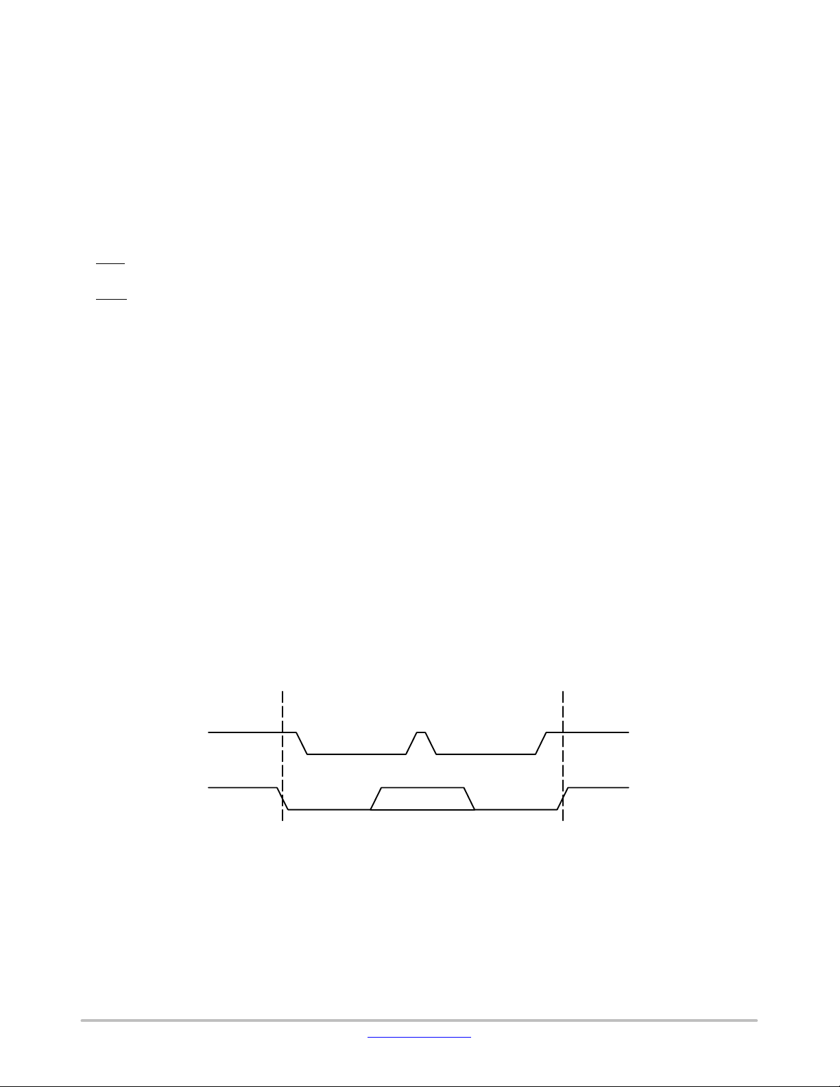
Figure 1. Functional Symbol
© Semiconductor Components Industries, LLC, 2017
April, 2019 − Rev. 2
ORDERING INFORMATION
See detailed ordering and shipping information on page 9 of
SDASCL
1 Publication Order Number:
this data sheet.
*For additional information on our Pb−Free strategy
and soldering details, please download the
ON Semiconductor Soldering and Mounting
Techniques Reference Manual, SOLDERRM/D.
N24S128/D
Page 2
N24S128
Table 1. ABSOLUTE MAXIMUM RATINGS
Parameter Rating Unit
Storage Temperature −65 to +150
Voltage on Any Pin with Respect to Ground (Note 1) −0.5 to +6.5 V
Stresses exceeding those listed in the Maximum Ratings table may damage the device. If any of these limits are exceeded, device functionality
should not be assumed, damage may occur and reliability may be affected.
1. The DC input voltage on any pin should not be lower than −0.5 V or higher than V
undershoot to no less than −1.5 V or overshoot to no more than V
+ 1.5 V, for periods of less than 20 ns.
CC
+ 1.0 V. During transitions, the voltage on any pin may
CC
Table 2. RELIABILITY CHARACTERISTICS (Note 2)
Symbol
N
(Note 3) Endurance 1,000,000 Program/Erase Cycles
END
T
(Note 4) Data Retention 100 Years
DR
2. These parameters are tested initially and after a design or process change that affects the parameter according to appropriate AEC−Q100
and JEDEC test methods.
3. Page Mode, V
= 55_C
4. T
A
= 5 V, 25_C
CC
Parameter Min Unit
Table 3. DC AND AC OPERATING CONDITIONS
Supply Voltage / Temperature Range Operation
V
= 1.7 V to 5.5 V / T
CC
V
= 1.6 V to 5.5 V / T
CC
V
= 1.6 V to 5.5 V / T
CC
= −40°C to +85°C
A
= −40°C to +85°C
A
= 0°C to +85°C
A
READ / WRITE
READ
WRITE
°C
Table 4. D.C. OPERATING CHARACTERISTICS
Symbol Parameter Test Conditions Min Max Unit
I
CCR
I
CCW
I
V
V
V
V
V
V
SB
I
L
IL1
IL2
IH1
IH2
OL1
OL2
Read Current
Write Current
Standby Current
I/O Pin Leakage
Input Low Voltage
Input Low Voltage V
Input High Voltage
Input High Voltage V
Output Low Voltage
Output Low Voltage
Read, f
All I/O Pins at GND or V
Pin at GND or V
V
CC
CC
V
CC
CC
V
CC
V
CC
= 400 kHz/1 MHz
SCL
1 mA
2 mA
V
V
CC
CC
< 2.5 V
> 2.5 V
−0.5 0.3 V
0.7 V
CC
CC
CC
CC
≥ 2.5 V
< 2.5 V −0.5 0.25 V
≥ 2.5 V
< 2.5 V 0.75 V
≥ 2.5 V, IOL = 3.0 mA
< 2.5 V, IOL = 1.0 mA
1 mA
2
2
V
CC
V
CC
0.4 V
0.2 V
CC
CC
+ 1 V
+ 1 V
mA
V
V
Product parametric performance is indicated in the Electrical Characteristics for the listed test conditions, unless otherwise noted. Product
performance may not be indicated by the Electrical Characteristics if operated under different conditions.
Table 5. PIN IMPEDANCE CHARACTERISTICS
Symbol Parameter Conditions Max Unit
C
(Note 5) SDA I/O Pin Capacitance V
IN
C
(Note 5) Input Capacitance (other pins) V
IN
5. These parameters are tested initially and after a design or process change that affects the parameter according to appropriate AEC−Q100
and JEDEC test methods.
= 0 V 8 pF
IN
= 0 V 6 pF
IN
www.onsemi.com
2
Page 3
N24S128
Table 6. A.C. CHARACTERISTICS (Note 6)
Standard
= 1.7 to 5.5
V
CC
= −40 to 855C
T
A
Symbol
F
SCL
t
HD:STA
t
LOW
t
HIGH
t
SU:STA
t
HD:DAT
t
SU:DAT
t
(Note 7) SDA and SCL Rise Time 1,000 20 300 100
R
t
(Note 7) SDA and SCL Fall Time 300 20 300 100
F
t
SU:STO
t
BUF
t
AA
t
DH
T
(Note 7) Noise Pulse Filtered at SCL and SDA Inputs 100 50 50
i
t
WR
T
PU
(Notes 7, 8)
Clock Frequency 100 400 1,000
START Condition Hold Time 4 0.6 0.26
Low Period of SCL Clock 4.7 1.3 0.5
High Period of SCL Clock 4 0.6 0.26
START Condition Setup Time 4.7 0.6 0.26
Data In Hold Time 0 0 0
Data In Setup Time 250 100 50
STOP Condition Setup Time 4 0.6 0.25
Bus Free Time Between STOP and START 4.7 1.3 0.5
SCL Low to Data Out Valid 3.5 0.9 0.40
Data Out Hold Time 100 100 50
Write Cycle Time 5 5 5
Power-up to Ready Mode 0.35 0.35 0.35
Parameter
Min Max Min Max Min Max
6. Test conditions according to “A.C. Test Conditions” table.
7. Tested initially and after a design or process change that affects this parameter.
is the delay between the time VCC is stable and the device is ready to accept commands.
8. t
PU
Fast
= 1.7 to 5.5
V
CC
= −40 to 855C
T
A
Fast−Plus
V
CC
= −40 to 855C
T
A
= 1.7 to 5.5
Unit
kHz
ms
ms
ms
ms
ms
ns
ns
ns
ms
ms
ms
ns
ns
ms
ms
Table 7. A.C. TEST CONDITIONS
Parameter Condition
Input Levels 0.2 × V
Input Rise and Fall Times
≤ 50 ns
to 0.8 × V
CC
Input Reference Levels 0.3 × VCC, 0.7 × V
Output Reference Levels 0.5 × V
Output Load
CC
Current Source: I
10
1
120 ns Rise Time
Pull-up Resistance (kW)
0.1
10
Load Capacitance (pF)
Figure 2. Maximum Pull-up Resistance vs. Load Capacitance
CC
CC
= 3 mA (V
OL
CC
300 ns Rise Time
100
≥ 2.5 V); I
= 1 mA (V
OL
< 2.5 V); C
CC
SDA
= 100 pF
L
V
CC
R
P
C
L
V
SS
www.onsemi.com
3
Page 4
N24S128
Power-On Reset (POR)
The N24S128 incorporates Power-On Reset (POR)
circuitry which protects the device against powering up in
the wrong state.
The N24S128 will power up into Standby mode after V
CC
exceeds the POR trigger level and will power down into
Reset mode when V
drops below the POR trigger level.
CC
This bi-directional POR feature protects the device against
‘brown-out’ failure following a temporary loss of power.
Pin Description
• SCL: The Serial Clock input pin accepts the Serial
Clock generated by the Master.
• SDA: The Serial Data I/O pin receives input data and
transmits data stored in EEPROM. In transmit mode,
this pin is open drain. Data is acquired on the positive
edge, and is delivered on the negative edge of SCL.
Functional Description
The N24S128 supports the Inter-Integrated Circuit (I2C)
Bus data transmission protocol, which defines a device that
sends data to the bus as a transmitter and a device receiving
data as a receiver. Data flow is controlled by a Master device,
which generates the serial clock and all START and STOP
conditions. The N24S128 acts as a Slave device. Master and
Slave alternate as either transmitter or receiver. Up to 8
devices may be connected to the bus as determined by the
Device Address bits A
Configuration Register.
2
C Bus Protocol
I
2
The I
C bus consists of two ‘wires’, SCL and SDA. The
two wires are connected to the V
resistors. Master and Slave devices connect to the 2-wire bus
via their respective SCL and SDA pins. The transmitting
device pulls down the SDA line to ‘transmit’ a ‘0’ and
releases it to ‘transmit’ a ‘1’.
, A1, and A2 in the Device
0
supply via pull-up
CC
Data transfer may be initiated only when the bus is not
busy (see A.C. Characteristics).
During data transfer, the SDA line must remain stable
while the SCL line is HIGH. An SDA transition while SCL
is HIGH will be interpreted as a START or STOP condition
(Figure 3). The START condition precedes all commands. It
consists of a HIGH to LOW transition on SDA while SCL
is HIGH. The START acts as a ‘wake-up’ call to all
receivers. Absent a START, a Slave will not respond to
commands. The STOP condition completes all commands.
It consists of a LOW to HIGH transition on SDA while SCL
is HIGH.
Device Addressing
The Master initiates data transfer by creating a START
condition on the bus. The Master then broadcasts an 8-bit
serial Slave address. The first 4 bits of the Slave address are
set to 1010, for normal Read/Write operations, and to 1011
for special Read/Write operations (Figure 4). The next 3 bits
must match the A2, A1, A0 bits in the Device Configuration
Register. The last bit, R/W, specifies whether a Read (1) or
Write (0) operation is to be performed.
The factory default for the A2, A1, A0 bits is 0.
Acknowledge
After processing the Slave address, the Slave responds
with an acknowledge (ACK) by pulling down the SDA line
during the 9
th
clock cycle (Figure 5). The Slave will also
acknowledge all address bytes and every data byte presented
in Write mode if the addressed location is not write
protected. In Read mode the Slave shifts out a data byte, and
then releases the SDA line during the 9
th
clock cycle. As
long as the Master acknowledges the data, the Slave will
continue transmitting. The Master terminates the session by
not acknowledging the last data byte (NoACK) and by
issuing a STOP condition. Bus timing is illustrated in
Figure 6.
SCL
SDA
START
CONDITION
STOP
CONDITION
Figure 3. START/STOP Conditions
www.onsemi.com
4
Page 5

N24S128
DEVICE ADDRESS
Memory Array Access 1 0 1 0 A2 A1 A0 R/W
SCL FROM
MASTER
DAT A OUTPUT
FROM TRANSMITTER
DAT A OUTPUT
FROM RECEIVER
Secure Data Page ,
1 0 1 1 A2 A1 A0 R/W
UID, Device Config.
Figure 4. Slave Address Bits
BUS RELEASE DELAY (TRANSMITTER) BUS RELEASE DELAY
189
START
ACK DELAY (≤ t
AA
)
ACK SETUP (≥ t
(RECEIVER)
Figure 5. Acknowledge Timing
t
F
t
LOW
t
HIGH
t
LOW
t
R
SU:DAT
)
SCL
SDA IN
SDA OUT
t
SU:STA
t
HD:STA
t
HD:DAT
t
AA
Figure 6. Bus Timing
t
SU:DAT
t
DH
t
SU:STO
t
BUF
www.onsemi.com
5
Page 6

N24S128
Write Operations
Byte Write
In Byte Write mode the Master sends a START, followed
by Slave address, two byte address (Table 8) and data to be
written (Figure 7). The Slave, N24S128 acknowledges all
4 bytes, and the Master then follows up with a STOP, which
in turn starts the internal Write operation (Figure 8). During
the internal Write cycle (t
), the N24S128 will not
WR
acknowledge any Read or Write request from the Master.
Page Write
The N24S128 contains 16,384 bytes of data, arranged in
256 pages of 64 bytes each. A two byte address word
(Table 8), following the Slave address, points to the first byte
to be written into the memory array. The most significant 8
bits from the address active bits (a13 to a6) identify the page
and the last 6 bits (a5 to a0) identify the byte within the page.
Up to 64 bytes can be written in one Write cycle (Figure 9).
The internal byte address counter is automatically
incremented after each data byte is loaded. If the Master
transmits more than 64 data bytes, then earlier bytes will be
overwritten by later bytes in a ‘wrap-around’ fashion (within
the selected page). The internal Write cycle starts
immediately following the STOP.
Acknowledge Polling
The ready/busy status of the N24S128 can be ascertained
by sending Read or Write requests immediately following
the STOP condition that initiated the internal Write cycle. As
long as internal Write is in progress, the N24S128 will not
acknowledge the Slave address.
The Device Configuration Register Write instruction does
not support acknowledge polling. Following this
instruction, the master must wait t
= 5 ms before sending
WR
a new instruction.
Secure Data Page Write
The Secure Data Page Write instruction is similar to a
Page Write instruction. To address the Secure Data Page, the
user must address the device with the header 1011 followed
by the A2 A1 A0 bits that match the bits in the Device
Configuration register. The second byte consists of xxxx
x00x, where x is don’t care. The third byte indicates the
address within the Secure Data Page. Since the page is
64-bytes wide, the first 2 bits of the address are don’t care.
The remainder of the instruction is identical to a normal
Page Write.
Secure Data Page Lock
The Secure Data Page Lock instruction is similar to a Byte
Write instruction. To lock the Secure Data Page against
future changes, the user must address the device with the
header 1011 followed by the A2 A1 A0 bits that match the
bits in the Device Configuration register. The second byte
consists of xxxx x10x, where x is don’t care. The third byte
is don’t care.
The data byte following the address bytes must be all 1s
(FFh). After this instruction is sent, the user will be able to
read, but not to write the content of the Secure Data Page.
Any write instructions to the Secure Data Page will return
No ACK from the device.
Device Configuration Register Write
The Device Configuration Register Write instruction is
similar to a Byte Write instruction. The user must address the
device with the header 1011b followed by the A2 A1 A0 bits
that match the bits in the Device Configuration register. The
second byte consists of xxxx x11x, where x is don’t care. The
third byte is don’t care.
The data byte following the address will be written into the
Device Configuration Register (see Table 9 for the position
of each bit.) The A2, A1, A0 bits determine the Device
Address.
The SWP bit is the Software Write Protection bit. When
SWP is set to 1, the memory array, the Secure Data Page and
the Device Configuration Register are protected against
write operations. The A2, A1, A0 bits cannot be overwritten
during a Device Configuration Register write operation if
SWP is set to 1. The SWP bit alone can be changed to 0.
The Device Configuration Register Write instruction does
not support acknowledge polling.
Table 8. MEMORY ADDRESS BYTES
A15 A14 A13 A12 A11 A10 A9 A8 A7 A6 A5 A4 A3 A2 A1 A0
Memory Array x x a13 a12 a11 a10 a9 a8 a7 a6 a5 a4 a3 a2 a1 a0
Secure Data Page
Secure Page Lock Bit
Unique ID Number
(read−only)
Device Configuration
x x x x x 0 0 x x x a5 a4 a3 a2 a1 a0
x x x x x 1 0 x x x x x x x x x
x x x x x 0 1 x x x x x 0 0 0 0
x x x x x 1 1 x x x x x x x x x
www.onsemi.com
6
Page 7

N24S128
Table 9. DEVICE CONFIGURATION REGISTER
b7 b6 b5 b4 b3 b2 b1 b0
A2 A1 A0 x x x SWP x
BUS ACTIVITY: S
MASTER
SLAVE
SCL
SDA
T
A
SLAVE
R
ADDRESS a
T
S
8th Bit
Byte n
A
C
K
ADDRESS
BYTE
13−a8
* *
ADDRESS
BYTE DATA
a7−a
A
C
K
Figure 7. Byte Write Sequence
ACK
STOP
CONDITION
Figure 8. Write Cycle Timing
S
T
0
t
WR
BYTE
AA
CC
KK
START
CONDITION
O
P
P
ADDRESS
BUS ACTIVITY: S
MASTER
SLAVE
T
A
R
T
S
P ≤
SLAVE
ADDRESS
63
A
C
K
ADDRESS
* *
A
C
K
ADDRESS
BYTE
a7−a
0
BYTE
a
13−a8
Figure 9. Page Write Sequence
DATA
BYTE
n
A
C
K
DATA
BYTE
n+1
A
C
K
A
C
K
DATA
BYTE
n+P
A
C
K
S
T
O
P
P
A
C
K
www.onsemi.com
7
Page 8

N24S128
Read Operations
Immediate Read
Upon receiving a Slave address with the R/W bit set to ‘1’,
the N24S128 will interpret this as a request for data residing
at the current byte address in memory. The N24S128 will
acknowledge the Slave address, will immediately shift out
the data residing at the current address, and will then wait for
the Master to respond. If the Master does not acknowledge
the data (NoACK) and then follows up with a STOP
condition (Figure 10), the N24S128 returns to Standby
mode.
Selective Read
To read data residing at a specific location, the internal
address counter must first be initialized as described under
Byte Write. If rather than following up the two address bytes
with data, the Master instead follows up with an Immediate
Read sequence, then the N24S128 will use the 14 active
address bits to initialize the internal address counter and will
shift out data residing at the corresponding location. If the
Master does not acknowledge the data (NoACK) and then
follows up with a STOP condition (Figure 11), the N24S128
returns to Standby mode.
Sequential Read
If during a Read session the Master acknowledges the 1
data byte, then the N24S128 will continue transmitting data
residing at subsequent locations until the Master responds
with a NoACK, followed by a STOP (Figure 12). In contrast
to Page Write, during Sequential Read the address count
will automatically increment to and then wrap-around at end
of memory (rather than end of page).
Secure Data Page Read
The Secure Data Page Read instruction is similar to
a Sequential Read instruction. To read data from a specific
location within the Secure Data Page, the address counter is
initialized by sending the device header and two address
bytes as for a Secure Data Page Write instruction. This
dummy write instruction is followed by an Immediate Read
with the device header 1011b, and the device will shift back
data from Secure Data Page. When the end of the Secure
Data Page is reached, the address counter will wrap-around
to zero, and the next byte returned will be the first byte in the
page.
Device Configuration Register Read
The Device Configuration Register Read instruction is
similar to a Selective Read instruction. The user must send
the device header and two address bytes as for a Device
Configuration Register Write instruction. This dummy write
instruction is followed by an Immediate Read with the
device header 1011b, and the device will shift back the
content of the Device Configuration Register. Don’t care
bits are read as 1s.
If the master acknowledges the data byte, requesting more
data, the device will continue to return the content of the
Device Configuration Register until the Master responds
with a NoACK.
Unique ID Number Read
The Unique ID Number Read instruction is similar to
a Sequential Read instruction. The user must send the device
header starting with 1011b followed by the A2 A1 A0 bits
that match the bits in the Device Configuration register. As
specified in Table 8, the second byte consists of xxxx x01x
and the third byte of xxxx 0000, where x is don’t care. This
dummy write instruction is followed by an Immediate Read
with the device header 1011b, and the device will shift back
the Unique ID byte by byte. The Unique ID is 16 bytes
(128 bits) long. After the last byte of the Unique ID has been
shifted, if the master acknowledges (requesting more data),
the device will wrap-around and start returning the Unique
ID from the beginning.
st
Secure Data Page Lock Status Read
There are two ways to check the lock status of the Security
Sector. The first way is to initiate a Secure Data Page Write.
The EEPROM will acknowledge if the Secure Data Page is
unlocked, and it will not acknowledge if the Secure Data
Page is locked. After the acknowledge bit, it is
recommended to generate a Start condition followed by
a Stop condition, to reset the interface.
The second way is to use a Lock Status Read instruction.
This instruction is similar to a Selective Read instruction,
but requires the use of the device address 1011b followed by
the A2, A1, A0 bits. The master first sends a dummy write
instruction followed by the address bytes specified in Table
8 (xxxx x10x xxxx xxxx, where x is don’t care). This is
followed by a read instruction using the same device address
as above. The device will return a data byte where Bit 1
indicates the lock status. If the lock is active this bit is “1”,
otherwise it is “0”.
Delivery State
The N24S128 is shipped erased, i.e., all memory array
bytes are FFh, and the settable Device Configuration bits set
to 0 (1Dh).
www.onsemi.com
8
Page 9

N24S128
SCL
SDA
BUS ACTIVIT Y:
MASTER
SLAVE
BU S ACTIVITY:
MASTER
SLAVE
8th Bit
DATA OUT NO ACK
S
T
A
R
T
S
89
AVE
SL
ADDRESS
A
DATA
C
K
BYTE
N
S
O
T
A
O
C
P
K
P
STOP
Figure 10. Immediate Read Sequence and Timing
SS
TT
AA
SLAVE
R
ADDRESS a
T
S
A
C
K
ADDRESS
BYTE
13−a8
* *
A
C
K
ADDRESS
BYTE
a7−a
0
A
C
KK
R
T
S
SLAVE
ADDRESS
A
DATA
C
BYTE
K
N
S
O
T
A
O
C
P
K
P
Figure 11. Selective Read Sequence
BUS ACTIVITY:
MASTER
SLAVE
SLAVE AT
ADDRESS C
A
DATA
C
BYTE
K
n
A
DATA
C
BYTE
K
n+1
A
DATA
C
BYTE
K
n+2
A
C
K
DATA
BYTE
n+x
N
O
KP
S
O
P
Figure 12. Sequential Read Sequence
Table 10. ORDERING INFORMATION (Notes 9 thru 11)
Device
Order Number
N24S128C4DYT3G P WLCSP 4-ball Industrial
†For information on tape and reel specifications, including part orientation and tape sizes, please refer to our Tape and Reel Packaging
Specifications Brochure, BRD8011/D.
9. All packages are RoHS-compliant (Lead-free, Halogen-free).
10.For detailed information and a breakdown of device nomenclature and numbering systems, please see the ON Semiconductor Device
Nomenclature document, TND310/D, available at www.onsemi.com
11. Caution: The EEPROM devices delivered in WLCSP must never be exposed to ultraviolet light. When exposed to ultraviolet light the
EEPROM cells lose their stored data.
Specific
Device Marking
Package
Type
Temperature
Range
(−40°C to +85°C)
Lead Finish Shipping
N/A 5,000 / Tape & Reel
†
ON Semiconductor is licensed by Philips Corporation to carry the I2C Bus Protocol.
www.onsemi.com
9
Page 10

WLCSP4, 0.84x0.84x0.3
8
MECHANICAL CASE OUTLINE
PACKAGE DIMENSIONS
SCALE 4:1
CASE 567VY
ISSUE O
DATE 21 FEB 201
GENERIC
MARKING DIAGRAM*
X
YW
X = Specific Device Code
Y = Year
W = Work Week
*This information is generic. Please refer to
device data sheet for actual part marking.
Pb−Free indicator, “G” or microdot “ G”,
may or may not be present. Some products
may not follow the Generic Marking.
DOCUMENT NUMBER:
DESCRIPTION:
ON Semiconductor and are trademarks of Semiconductor Components Industries, LLC dba ON Semiconductor or its subsidiaries in the United States and/or other countries.
ON Semiconductor reserves the right to make changes without further notice to any products herein. ON Semiconductor makes no warranty, representation or guarantee regarding
the suitability of its products for any particular purpose, nor does ON Semiconductor assume any liability arising out of the application or use of any product or circuit, and specifically
disclaims any and all liability, including without limitation special, consequential or incidental damages. ON Semiconductor does not convey any license under its patent rights nor the
rights of others.
© Semiconductor Components Industries, LLC, 2018
98AON83936G
WLCSP4, 0.84x0.84x0.3
Electronic versions are uncontrolled except when accessed directly from the Document Repository.
Printed versions are uncontrolled except when stamped “CONTROLLED COPY” in red.
PAGE 1 OF 1
www.onsemi.com
Page 11

ON Semiconductor and are trademarks of Semiconductor Components Industries, LLC dba ON Semiconductor or its subsidiaries in the United States and/or other countries.
ON Semiconductor owns the rights to a number of patents, trademarks, copyrights, trade secrets, and other intellectual property. A listing of ON Semiconductor’s product/patent
coverage may be accessed at www.onsemi.com/site/pdf/Patent−Marking.pdf
ON Semiconductor makes no warranty, representation or guarantee regarding the suitability of its products for any particular purpose, nor does ON Semiconductor assume any liability
arising out of the application or use of any product or circuit, and specifically disclaims any and all liability, including without limitation special, consequential or incidental damages.
Buyer is responsible for its products and applications using ON Semiconductor products, including compliance with all laws, regulations and safety requirements or standards,
regardless of any support or applications information provided by ON Semiconductor. “Typical” parameters which may be provided in ON Semiconductor data sheets and/or
specifications can and do vary in different applications and actual performance may vary over time. All operating parameters, including “Typicals” must be validated for each customer
application by customer’s technical experts. ON Semiconductor does not convey any license under its patent rights nor the rights of others. ON Semiconductor products are not
designed, intended, or authorized for use as a critical component in life support systems or any FDA Class 3 medical devices or medical devices with a same or similar classification
in a foreign jurisdiction or any devices intended for implantation in the human body. Should Buyer purchase or use ON Semiconductor products for any such unintended or unauthorized
application, Buyer shall indemnify and hold ON Semiconductor and its officers, employees, subsidiaries, affiliates, and distributors harmless against all claims, costs, damages, and
expenses, and reasonable attorney fees arising out of, directly or indirectly, any claim of personal injury or death associated with such unintended or unauthorized use, even if such
claim alleges that ON Semiconductor was negligent regarding the design or manufacture of the part. ON Semiconductor is an Equal Opportunity/Affirmative Action Employer. This
literature is subject to all applicable copyright laws and is not for resale in any manner.
. ON Semiconductor reserves the right to make changes without further notice to any products herein.
PUBLICATION ORDERING INFORMATION
LITERATURE FULFILLMENT:
Email Requests to: orderlit@onsemi.com
ON Semiconductor Website: www.onsemi.com
TECHNICAL SUPPORT
North American Technical Support:
Voice Mail: 1 800−282−9855 Toll Free USA/Canada
Phone: 011 421 33 790 2910
Europe, Middle East and Africa Technical Support:
Phone: 00421 33 790 2910
For additional information, please contact your local Sales Representative
◊
www.onsemi.com
1
 Loading...