

Page 1
查询MZP4729ATA供应商
MZP4729A Series
3 Watt DO−41 SurmeticE 30
Zener Voltage Regulators
This is a complete series of 3 Watt Zener diodes with limits and
excellent operating characteristics that reflect the superior capabilities
of silicon−oxide passivated junctions. All this in an axial−lead,
transfer−molded plastic package that offers protection in all common
environmental conditions.
http://onsemi.com
Specification Features:
• Zener Voltage Range − 3.6 V to 30 V
• ESD Rating of Class 3 (>16 KV) per Human Body Model
• Surge Rating of 98 W @ 1 ms
• Maximum Limits Guaranteed on up to Six Electrical Parameters
• Package No Larger than the Conventional 1 Watt Package
w These devices are available in Pb−free package(s). Specifications herein
apply to both standard and Pb−free devices. Please see our website at
www.onsemi.com for specific Pb−free orderable part numbers, or
contact your local ON Semiconductor sales office or representative.
Mechanical Characteristics:
Void free, transfer−molded, thermosetting plastic
CASE:
FINISH: All external surfaces are corrosion resistant and leads are
readily solderable
MAXIMUM LEAD TEMPERATURE FOR SOLDERING PURPOSES:
230°C, 1/16″ from the case for 10 seconds
POLARITY: Cathode indicated by polarity band
MOUNTING POSITION: Any
MAXIMUM RATINGS
Rating Symbol Value Unit
Max. Steady State Power Dissipation
= 75°C, Lead Length = 3/8″
@ T
L
Derate above 75°C
Steady State Power Dissipation
= 50°C
@ T
A
Derate above 50°C
Operating and Storage
Temperature Range
P
P
TJ, T
D
D
stg
3
24
1
6.67
−65 to
+200
W
mW/°C
W
mW/°C
°C
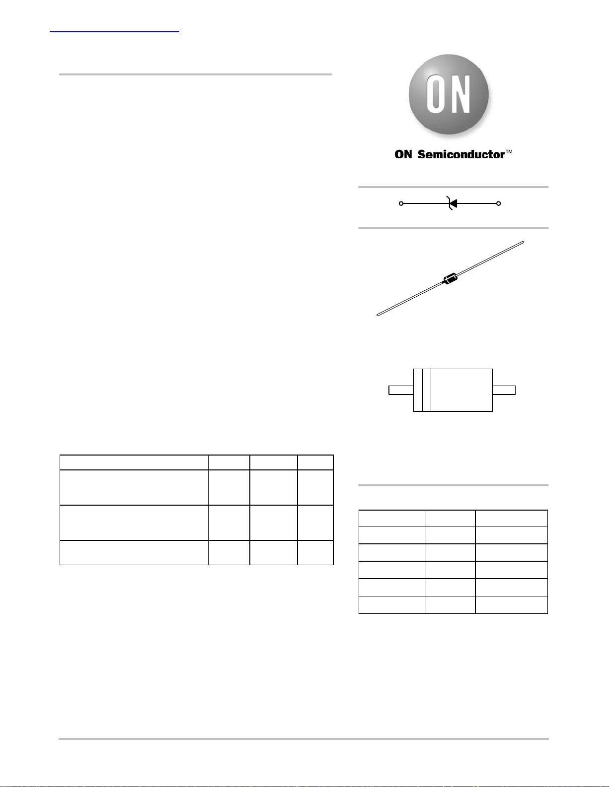
Cathode Anode
AXIAL LEAD
CASE 59
PLASTIC
MARKING DIAGRAM
L
MZP4
7xxA
YYWW
L = Assembly Location
MZP47xxA = Device Code
YY = Year
WW = Work Week
= (See Table Next Page)
ORDERING INFORMATION
Device Package Shipping
MZP47xxA Axial Lead 2000 Units/Box
MZP47xxARL Axial Lead
MZP47xxATA Axial Lead 4000/Ammo Pack
{
MZP47xxARR1
MZP47xxARR2
{
Polarity band up with cathode lead off first
}
Polarity band down with cathode lead off first
Axial Lead 2000/Tape & Reel
}
Axial Lead 2000/Tape & Reel
6000/Tape & Reel
© Semiconductor Components Industries, LLC, 2006
March, 2006 − Rev. 3
1 Publication Order Number:
MZP4729A/D
Page 2
MZP4729A Series
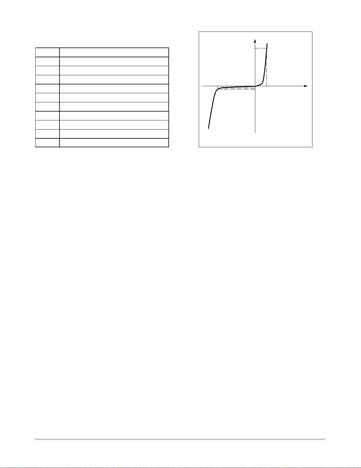
ELECTRICAL CHARACTERISTICS (T
otherwise noted, V
Symbol
V
Z
I
ZT
Z
ZT
I
ZK
Z
ZK
I
R
V
R
I
F
V
F
I
R
= 1.5 V Max @ IF = 200 mA for all types)
F
Parameter
Reverse Zener Voltage @ I
ZT
Reverse Current
Maximum Zener Impedance @ I
Reverse Current
Maximum Zener Impedance @ I
Reverse Leakage Current @ V
Breakdown Voltage
Forward Current
Forward Voltage @ I
F
Surge Current @ TA = 25°C
= 25°C unless
A
ZT
ZK
R
I
I
F
VRV
Z
I
V
R
I
ZT
Zener Voltage Regulator
V
F
http://onsemi.com
2
Page 3
MZP4729A Series
ELECTRICAL CHARACTERISTICS (T
= 25°C unless otherwise noted, VF = 1.5 V Max @ IF = 200 mA for all types)
A
Zener Voltage (Note 2) Zener Impedance (Note 3) Leakage Current
Device
(Note 1)
Device
Marking
VZ (Volts) @ IZTZZT @ I
Min Nom Max mA
W W
ZZK @ I
ZT
ZK
IR @ V
R
(Note 4)
mA μA Max Volts mA
MZP4729A MZP4729A 3.42 3.6 3.78 69 10 400 1 100 1 1260
MZP4734A MZP4734A 5.32 5.6 5.88 45 5 600 1 10 2 810
MZP4735A MZP4735A 5.89 6.2 6.51 41 2 700 1 10 3 730
MZP4736A MZP4736A 6.46 6.8 7.14 37 3.5 700 1 10 4 660
MZP4737A MZP4737A 7.13 7.5 7.88 34 4 700 0.5 10 5 605
MZP4738A MZP4738A 7.79 8.2 8.61 31 4.5 700 0.5 10 6 550
MZP4740A MZP4740A 9.50 10 10.50 25 7 700 0.25 10 7.6 454
MZP4741A MZP4741A 10.45 11 11.55 23 8 700 0.25 5 8.4 414
MZP4744A MZP4744A 14.25 15 15.75 17 14 700 0.25 5 11.4 304
MZP4745A MZP4745A 15.20 16 16.80 15.5 16 700 0.25 5 12.2 285
MZP4746A MZP4746A 17.10 18 18.90 14 20 750 0.25 5 13.7 250
MZP4749A MZP4749A 22.80 24 25.20 10.5 25 750 0.25 5 18.2 190
MZP4750A MZP4750A 25.65 27 28.35 9.5 35 750 0.25 5 20.6 170
MZP4751A MZP4751A 28.50 30 31.50 8.5 40 1000 0.25 5 22.8 150
MZP4752A MZP4752A 31.35 33 34.65 7.5 45 1000 0.25 5 25.1 135
MZP4753A MZP4753A 34.20 36 37.80 7.0 50 1000 0.25 5 27.4 125
1. TOLERANCE AND TYPE NUMBER DESIGNATION
The type numbers listed have a standard tolerance on the nominal zener voltage of ±5%.
2. ZENER VOLTAGE (V
ON Semiconductor guarantees the zener voltage when measured at 90 seconds while maintaining the lead temperature (T
3/8″ from the diode body.
3. ZENER IMPEDANCE (Z
The zener impedance is derived from 60 seconds AC voltage, which results when an AC current having an rms value equal to 10% of the
DC zener current (I
4. SURGE CURRENT (I
The rating listed in the electrical characteristics table is maximum peak, non−repetitive, reverse surge current of 1/2 square wave or
equivalent sine wave pulse of 1/120 second duration superimposed on the test current, I
capability is as described in Figure 3 of the General Data sheet for Surmetic 30s.
) MEASUREMENT
Z
) DERIVATION
Z
or IZK) is superimposed on IZT or IZK.
ZT
) NON−REPETITIVE
R
) at 30°C ±1°C,
L
, per JEDEC standards. However, actual device
ZT
I
R
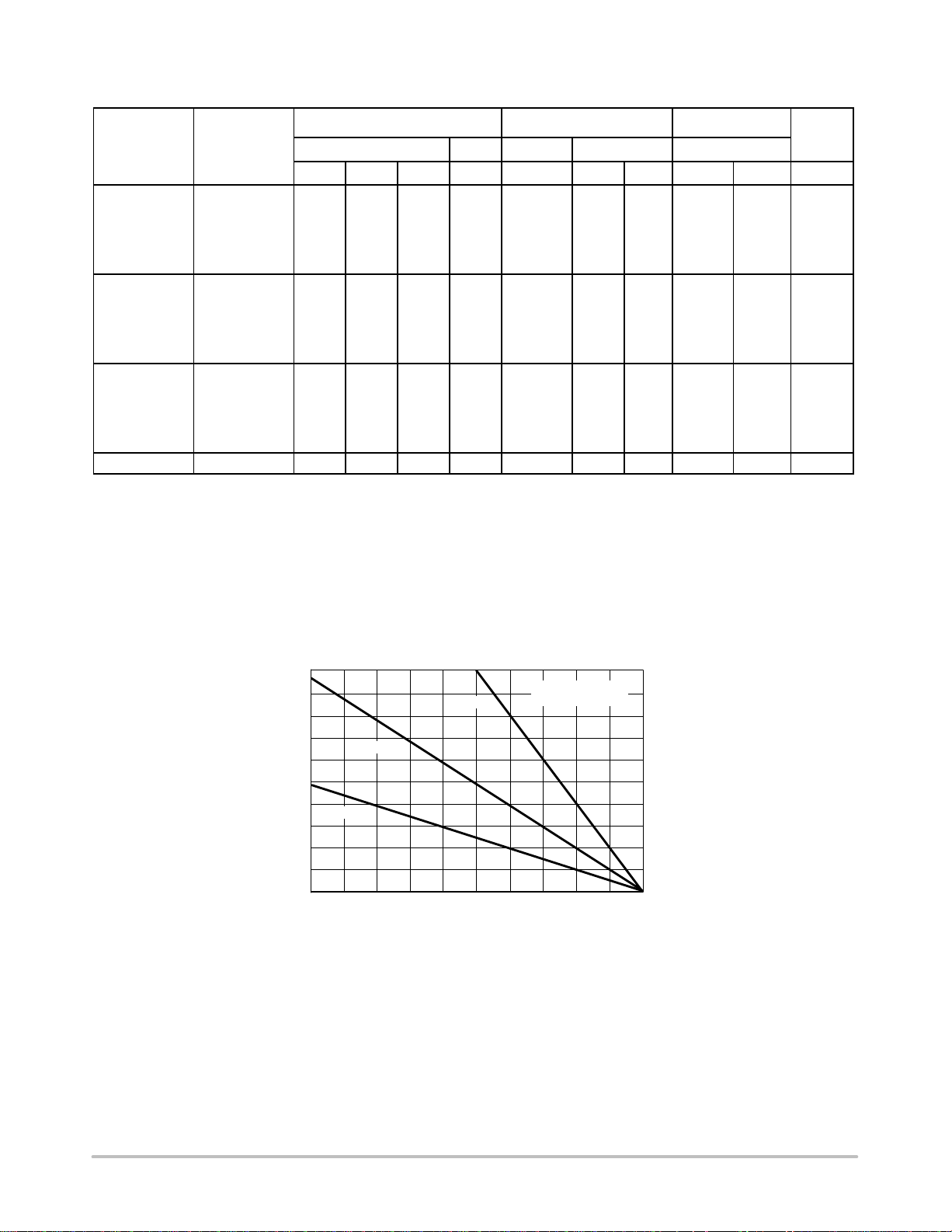
5
L = 1/8″
4
3
2
1
, MAXIMUM STEADY STATE
D
P
POWER DISSIPATION (WATTS)
0
0 20 40 60 20080 100 120 140 160 180
L = 3/8″
L = 1″
TL, LEAD TEMPERATURE (°C)
Figure 1. Power Temperature Derating Curve
L = LEAD LENGTH
TO HEAT SINK
http://onsemi.com
3
Page 4

MZP4729A Series
30
20
D =0.5
10
7
0.2
5
0.1
0.05
0.02
0.01
D = 0
NOTE: BELOW 0.1 SECOND, THERMAL
RESPONSE CURVE IS APPLICABLE
TO ANY LEAD LENGTH (L).
t
P
1
PK
t
2
DUTY CYCLE, D =t1/t
SINGLE PULSE ΔTJL = θJL (t)P
REPETITIVE PULSES ΔTJL = θJL (t,D)P
PK
JUNCTION-TO-LEAD ( C/W)°
0.7
0.5
(t, D) TRANSIENT THERMAL RESISTANCE
JL
θ
0.3
3
2
1
0.0001 0.0002 0.0005 0.001 0.002 0.005 0.01 0.02 0.05 0.1 0.2 0.5 1 2 5 10
t, TIME (SECONDS)
Figure 2. Typical Thermal Response L, Lead Length = 3/8 Inch
1K
RECTANGULAR
500
300
200
NONREPETITIVE
WAVEFORM
=25°C PRIOR
T
J
TO INITIAL PULSE
100
50
30
PK
20
P , PEAK SURGE POWER (WATTS)
10
0.1 0.2 0.3 0.5 1 2 3 5 10 20 30 50 100
PW, PULSE WIDTH (ms)
, REVERSE LEAKAGE (μ Adc) @ V
I
R
R
3
2
1
0.5
0.2
0.1
0.05
0.02
0.01
0.005
0.002
0.001
AS SPECIFIED IN ELEC. CHAR. TABLE
0.0005
0.0003
1 2 5 10 20 50 100 200 400 1000
NOMINAL V
(VOLTS)
Z
TA = 125°C
TA = 125°C
Figure 3. Maximum Surge Power Figure 4. Typical Reverse Leakage
2
PK
http://onsemi.com
4
Page 5

APPLICATION NOTE
MZP4729A Series
Since the actual voltage available from a given zener
diode is temperature dependent, it is necessary to determine
junction temperature under any set of operating conditions
in order to calculate its value. The following procedure is
recommended:
Lead Temperature, T
, should be determined from:
L
TL = θLA PD + T
A
θLA is the lead-to-ambient thermal resistance (°C/W) and P
is the power dissipation. The value for θLA will vary and
depends on the device mounting method. θ
is generally
LA
30−40°C/W for the various clips and tie points in common
use and for printed circuit board wiring.
The temperature of the lead can also be measured using a
thermocouple placed on the lead as close as possible to the
tie point. The thermal mass connected to the tie point is
normally large enough so that it will not significantly
respond to heat surges generated in the diode as a result of
pulsed operation once steady-state conditions are achieved.
Using the measured value of T
, the junction temperature
L
may be determined by:
TJ = TL + ΔT
JL
ΔTJL is the increase in junction temperature above the lead
temperature and may be found from Figure 2 for a train of
power pulses (L = 3/8 inch) or from Figure 10 for dc power.
ΔTJL = θJL P
D
For worst-case design, using expected limits of IZ, limits
of P
and the extremes of TJ (ΔTJ) may be estimated.
D
Changes in voltage, V
D
, can then be found from:
Z
ΔV = θVZ ΔT
J
θVZ, the zener voltage temperature coefficient, is found
from Figures 5 and 6.
Under high power-pulse operation, the zener voltage will
vary with time and may also be affected significantly by the
zener resistance. For best regulation, keep current
excursions as low as possible.
Data of Figure 2 should not be used to compute surge
capability. Surge limitations are given in Figure 3. They are
lower than would be expected by considering only junction
temperature, as current crowding effects cause temperatures
to be extremely high in small spots resulting in device
degradation should the limits of Figure 3 be exceeded.
http://onsemi.com
5
Page 6

MZP4729A Series
TEMPERATURE COEFFICIENT RANGES
(90% of the Units are in the Ranges Indicated)
ZTVZ
10
°
8
ZTVZ
°θ
1000
500
6
4
2
0
−2
, TEMPERATURE COEFFICIENT (mV/ C) @ I
−4
θ
34 5 6789101112
VZ, ZENER VOLTAGE @ IZT (VOLTS)
RANGE
Figure 5. Units To 12 Volts Figure 6. Units 10 To 400 Volts
ZENER VOLTAGE versus ZENER CURRENT
(Figures 7, 8 and 9)
100
50
30
20
10
5
3
2
1
Z
I , ZENER CURRENT (mA)
0.5
0.3
0.2
0.1
01234 567 8910
, ZENER VOLTAGE (VOLTS)
V
Z
Figure 7. V
= 3.3 thru 10 Volts Figure 8. VZ = 12 thru 82 Volts
Z
200
100
50
20
, TEMPERATURE COEFFICIENT (mV/ C) @ I
10
10 20 50 100 200 400 1000
V
, ZENER VOLTAGE @ IZT (VOLTS)
Z
100
50
30
20
10
5
3
2
1
Z
I , ZENER CURRENT (mA)
0.5
0.3
0.2
0.1
0102030405060708090100
, ZENER VOLTAGE (VOLTS)
V
Z
10
5
2
1
0.5
Z
I , ZENER CURRENT (mA)
0.2
0.1
100 200 300 400250 350150
, ZENER VOLTAGE (VOLTS)
V
Z
Figure 9. V
Z
80
( C/W)°
70
60
50
40
30
T
20
10
0
0 1/8 1/4 3/8 1/2 5/8 3/4 7/8 1
, JUNCTION-TO-LEAD THERMAL RESISTANCE
JL
θ
L, LEAD LENGTH TO HEAT SINK (INCH)
PRIMARY PATH OF
CONDUCTION IS THROUGH
THE CATHODE LEAD
L
= 100 thru 400 Volts Figure 10. Typical Thermal Resistance
http://onsemi.com
6
LL
Page 7

MZP4729A Series
OUTLINE DIMENSIONS
Zener Voltage Regulators − Axial Leaded
3 Watt DO−41 SurmeticE 30
PLASTIC DO−41
CASE 59−10
ISSUE R
NOTES:
B
K
D
F
A
F
K
1. DIMENSIONING AND TOLERANCING PER ANSI
Y14.5M, 1982.
2. CONTROLLING DIMENSION: INCH.
3. 59−04 OBSOLETE, NEW STANDARD 59−09.
4. 59−03 OBSOLETE, NEW STANDARD 59−10.
5. ALL RULES AND NOTES ASSOCIATED WITH
JEDEC DO−41 OUTLINE SHALL APPLY
6. POLARITY DENOTED BY CATHODE BAND.
7. LEAD DIAMETER NOT CONTROLLED WITHIN F
DIMENSION.
DIM MIN MAX MIN MAX
A 4.10 5.200.161 0.205
B 2.00 2.700.079 0.106
D 0.71 0.860.028 0.034
F −−− 1.27−−− 0.050
K 25.40 −−−1.000 −−−
MILLIMETERSINCHES
Surmetic is a trademark of Semiconductor Components Industries, LLC.
ON Semiconductor and are registered trademarks of Semiconductor Components Industries, LLC (SCILLC). SCILLC reserves the right to make changes without further notice
to any products herein. SCILLC makes no warranty, representation or guarantee regarding the suitability of its products for any particular purpose, nor does SCILLC assume any liability
arising out of the application or use of any product or circuit, and specifically disclaims any and all liability, including without limitation special, consequential or incidental damages.
“Typical” parameters which may be provided in SCILLC data sheets and/or specifications can and do vary in different applications and actual performance may vary over time. All
operating parameters, including “Typicals” must be validated for each customer application by customer’s technical experts. SCILLC does not convey any license under its patent rights
nor the rights of others. SCILLC products are not designed, intended, or authorized for use as components in systems intended for surgical implant into the body, or other applications
intended to support or sustain life, or for any other application in which the failure of the SCILLC product could create a situation where personal injury or death may occur. Should
Buyer purchase or use SCILLC products for any such unintended or unauthorized application, Buyer shall indemnify and hold SCILLC and its officers, employees, subsidiaries, affiliates,
and distributors harmless against all claims, costs, damages, and expenses, and reasonable attorney fees arising out of, directly or indirectly, any claim of personal injury or death
associated with such unintended or unauthorized use, even if such claim alleges that SCILLC was negligent regarding the design or manufacture of the part. SCILLC is an Equal
Opportunity/Affirmative Action Employer. This literature is subject to all applicable copyright laws and is not for resale in any manner.
PUBLICATION ORDERING INFORMATION
LITERATURE FULFILLMENT:
Literature Distribution Center for ON Semiconductor
P.O. Box 61312, Phoenix, Arizona 85082−1312 USA
Phone: 480−829−7710 or 800−344−3860 Toll Free USA/Canada
Fax: 480−829−7709 or 800−344−3867 Toll Free USA/Canada
Email: orderlit@onsemi.com
N. American Technical Support: 800−282−9855 Toll Free
USA/Canada
Japan: ON Semiconductor, Japan Customer Focus Center
2−9−1 Kamimeguro, Meguro−ku, Tokyo, Japan 153−0051
Phone: 81−3−5773−3850
http://onsemi.com
ON Semiconductor Website: http://onsemi.com
Order Literature: http://www.onsemi.com/litorder
For additional information, please contact your
local Sales Representative.
MZP4729A/D
7
 Loading...