

Page 1
MUR120 Series
Preferred Devices
SWITCHMODEt
Power Rectifiers
MUR105, MUR110, MUR115, MUR120,
MUR130, MUR140, MUR160
The MUR120 series of SWITCHMODE power rectifiers are
designed for use in switching power supplies, inverters and as free
wheeling diodes.
Features
• Ultrafast 25, 50 and 75 Nanosecond Recovery Times
• 175°C Operating Junction Temperature
• Low Forward Voltage
• Low Leakage Current
• High Temperature Glass Passivated Junction
• Reverse Voltage to 600 V
• Shipped in Plastic Bags; 1,000 per Bag
• Available Tape and Reel; 5,000 per Reel, by adding a “RL’’ Suffix to
the Part Number
• These are Pb−Free Devices*
http://onsemi.com
ULTRAFAST RECTIFIERS
1.0 AMPERE, 50 − 600 VOLTS
Mechanical Characteristics:
• Case: Epoxy, Molded
• Weight: 0.4 Gram (Approximately)
• Finish: All External Surfaces Corrosion Resistant and Terminal
Leads are Readily Solderable
• Lead Temperature for Soldering Purposes:
260°C Max. for 10 Seconds
• Polarity: Cathode Indicated by Polarity Band
*For additional information on our Pb−Free strategy and soldering details, please
download the ON Semiconductor Soldering and Mounting Techniques
Reference Manual, SOLDERRM/D.
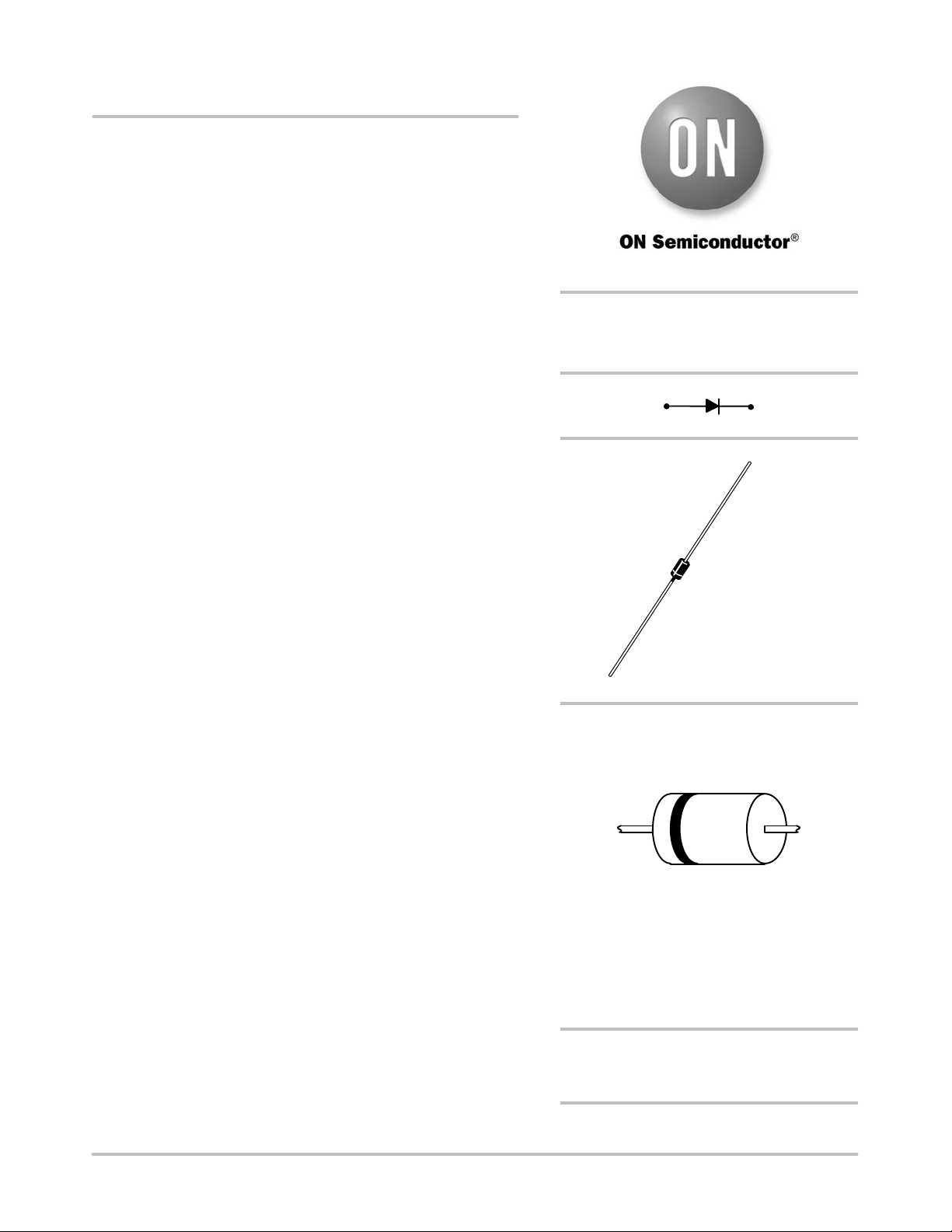
AXIAL LEAD
CASE 59
STYLE 1
MARKING DIAGRAM
A
MUR
1xx
YYWW G
G
A = Assembly Location
MUR1xx= Specific Device Code
Y = Year
WW = Work Week
G = Pb−Free Package
(Note: Microdot may be in either location)
ORDERING INFORMATION
See detailed ordering and shipping information in the package
dimensions section on page 6 of this data sheet.
Preferred devices are recommended choices for future use
and best overall value.
© Semiconductor Components Industries, LLC, 2006
July, 2006 − Rev. 10
1 Publication Order Number:
MUR120/D
Page 2
MUR120 Series
MAXIMUM RATINGS
MUR
Rating Symbol
Peak Repetitive Reverse Voltage
Working Peak Reverse Voltage
DC Blocking Voltage
Average Rectified Forward Current
(Square Wave Mounting Method #3 Per Note 2)
Nonrepetitive Peak Surge Current
(Surge applied at rated load conditions, halfwave,
V
RRM
V
RWM
V
I
F(AV)
I
FSM
single phase, 60 Hz)
Operating Junction Temperature and Storage Temperature TJ, T
Stresses exceeding Maximum Ratings may damage the device. Maximum Ratings are stress ratings only. Functional operation above the
Recommended Operating Conditions is not implied. Extended exposure to stresses above the Recommended Operating Conditions may affect
device reliability.
THERMAL CHARACTERISTICS
Characterisic Symbol Max Unit
Maximum Thermal Resistance, Junction−to−Ambient
R
q
ELECTRICAL CHARACTERISTICS
Maximum Instantaneous Forward Voltage (Note 1)
(iF = 1.0 Amp, TJ = 150°C)
(iF = 1.0 Amp, TJ = 25°C)
Maximum Instantaneous Reverse Current (Note 1)
(Rated DC Voltage, TJ = 150°C)
(Rated DC Voltage, TJ = 25°C)
Maximum Reverse Recovery Time
(IF = 1.0 A, di/dt = 50 A/ms)
(IF = 0.5 A, iR = 1.0 A, I
REC
= 0.25 A)
Maximum Forward Recovery Time
(IF = 1.0 A, di/dt = 100 A/ms, I
REC
to 1.0 V)
1. Pulse Test: Pulse Width = 300 ms, Duty Cycle ≤ 2.0%.
v
i
R
t
rr
t
fr
105 110 115 120 130 140 160
50 100 150 200 300 400 600 V
R
1.0 @ TA = 130°C 1.0 @ TA = 120°C A
35 A
stg
JA
F
*65 to +175 °C
Note 2 °C/W
0.710
0.875
50
2.0
35
25
25 50 ns
Unit
V
1.05
1.25
mA
150
5.0
ns
75
50
http://onsemi.com
2
Page 3
MUR120 Series
MUR105, MUR110, MUR115, MUR120
10
7.0
5.0
3.0
2.0
1.0
0.7
0.5
0.3
0.2
, INSTANTANEOUS FORWARD CURRENT (AMPS)
F
i
0.1
0.07
0.05
= 175°C
J
25°C
100
TJ = 175°C
10
m
1.0
100°CT
0.1
, REVERSE CURRENT ( A)
R
I
0.01
0.001
06040 100 120
20 80 200
VR, REVERSE VOLTAGE (VOLTS)
100°C
25°C
160 180140
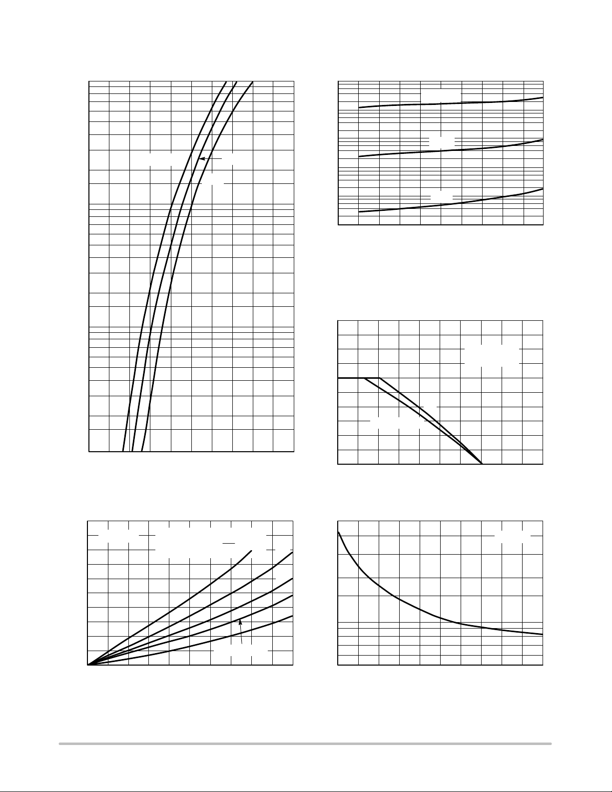
Figure 2. Typical Reverse Current*
* The curves shown are typical for the highest voltage device in the
voltage grouping. Typical reverse current for lower voltage selections
can be estimated from these same curves if VR is sufficiently below
rated VR.
5.0
4.0
3.0
RATED V
R
q
JA
R
= 50°C/W
0.03
0.02
0.01
0.3 0.60.4 0.8
0.5
v
INSTANTANEOUS VOLTAGE (VOLTS)
F,
Figure 1. Typical Forward Voltage
5.0
TJ = 175°C
4.0
3.0
2.0
1.0
, AVERAGE POWER DISSIPATION (WATTS)
F(AV)
0
P
0
0.5 1.0 1.5 2.0 2.5
I
, AVERAGE FORWARD CURRENT (AMPS)
F(AV)
Figure 4. Power Dissipation
0.7 0.9 1.1
(CAPACITIVELOAD)
1.0 1.2
I
PK
I
AV
SQUARE WAVE
+ 20
10
5.0
dc
1.3
2.0
1.0
, AVERAGE FORWARD CURRENT (AMPS)
0
F(AV)
I
050
50
30
20
10
C, CAPACITANCE (pF)
7.0
5.0
0
dc
SQUARE WAVE
150100 200
TA, AMBIENT TEMPERATURE (°C)
Figure 3. Current Derating
(Mounting Method #3 Per Note 1)
TJ = 25°C
10 20
VR, REVERSE VOLTAGE (VOLTS)
30 40 50
Figure 5. Typical Capacitance
250
http://onsemi.com
3
Page 4

MUR120 Series
MUR130, MUR140, MUR160
10
7.0
5.0
3.0
2.0
1.0
0.7
0.5
0.3
0.2
, INSTANTANEOUS FORWARD CURRENT (AMPS)
F
i
0.1
0.07
0.05
T
J
= 175°C
25°C
100°C
400
100
40
m
10
4.0
1.0
0.4
0.1
, REVERSE CURRENT ( A)
R
I
0.04
0.01
0.004
0 200100 300 400
VR, REVERSE VOLTAGE (VOLTS)
TJ = 175°C
100°C
25°C
Figure 7. Typical Reverse Current*
* The curves shown are typical for the highest voltage device in the
voltage grouping. Typical reverse current for lower voltage selections
can be estimated from these same curves if VR is sufficiently below
rated VR.
5.0
4.0
3.0
RATED V
R
q
JA
R
= 50°C/W
700
600500
0.03
0.02
0.01
0.3 0.90.5 1.3
0.7
v
INSTANTANEOUS VOLTAGE (VOLTS)
F,
Figure 6. Typical Forward Voltage
5.0
TJ = 175°C
4.0
, AVERAGE POWER DISSIPATION (WATTS)
F(AV)
P
3.0
2.0
1.0
0
0
(CAPACITIVE LOAD)
I
PK
I
AV
0.5 1.0 1.5 2.0 2.5
I
, AVERAGE FORWARD CURRENT (AMPS)
F(AV)
Figure 9. Power Dissipation
1.1 1.5 1.9
10
+ 20
1.7 2.1
5.0
SQUARE WAVE
2.3
2.0
1.0
, AVERAGE FORWARD CURRENT (AMPS)
0
F(AV)
I
050
SQUARE WAVE
TA, AMBIENT TEMPERATURE (°C)
dc
150100 200
250
Figure 8. Current Derating
(Mounting Method #3 Per Note 2)
20
TJ = 25°C
10
7.0
dc
C, CAPACITANCE (pF)
5.0
3.0
2.0
0
10 20
VR, REVERSE VOLTAGE (VOLTS)
30 40 50
Figure 10. Typical Capacitance
http://onsemi.com
4
Page 5

MUR120 Series
NOTE 2. — AMBIENT MOUNTING DATA
Data shown for thermal resistance, junction−to−ambient
(R
) for the mountings shown is to be used as typical
qJA
guideline values for preliminary engineering or in case the
tie point temperature cannot be measured.
TYPICAL VALUES FOR R
Mounting
Method
1
2
3
R
q
JA
MOUNTING METHOD 1
L L
MOUNTING METHOD 2
L L
Lead Length, L
1/8 1/4 1/2 Units
52
67
IN STILL AIR
q
JA
65 72
80 87
50
°C/W
°C/W
°C/W
Vector Pin Mounting
MOUNTING METHOD 3
L = 3/8
Board Ground Plane
P.C. Board with
1−1/2 X 1−1/2 Copper Surface″″
http://onsemi.com
5
″
Page 6

MUR120 Series
ORDERING INFORMATION
Device Marking Package Shipping
MUR105 MUR105 Axial Lead* 1000 Units / Bag
MUR105G MUR105 Axial Lead* 1000 Units / Bag
MUR105RL MUR105 Axial Lead* 5000 Units / Tape & Reel
MUR105RLG MUR105 Axial Lead* 5000 Units / Tape & Reel
MUR110 MUR110 Axial Lead* 1000 Units / Bag
MUR110G MUR110 Axial Lead* 1000 Units / Bag
MUR110RL MUR110 Axial Lead* 5000 Units / Tape & Reel
MUR110RLG MUR110 Axial Lead* 5000 Units / Tape & Reel
MUR115 MUR115 Axial Lead* 1000 Units / Bag
MUR115G MUR115 Axial Lead* 1000 Units / Bag
MUR115RL MUR115 Axial Lead* 5000 Units / Tape & Reel
MUR115RLG MUR115 Axial Lead* 5000 Units / Tape & Reel
MUR120 MUR120 Axial Lead* 1000 Units / Bag
MUR120G MUR120 Axial Lead* 1000 Units / Bag
MUR120RL MUR120 Axial Lead* 5000 Units / Tape & Reel
MUR120RLG MUR120 Axial Lead* 5000 Units / Tape & Reel
MUR130 MUR130 Axial Lead* 1000 Units / Bag
MUR130G MUR130 Axial Lead* 1000 Units / Bag
MUR130RL MUR130 Axial Lead* 5000 Units / Tape & Reel
MUR130RLG MUR130 Axial Lead* 5000 Units / Tape & Reel
MUR140 MUR140 Axial Lead* 1000 Units / Bag
MUR140G MUR140 Axial Lead* 1000 Units / Bag
MUR140RL MUR140 Axial Lead* 5000 Units / Tape & Reel
MUR140RLG MUR140 Axial Lead* 5000 Units / Tape & Reel
MUR160 MUR160 Axial Lead* 1000 Units / Bag
MUR160G MUR160 Axial Lead* 1000 Units / Bag
MUR160RL MUR160 Axial Lead* 5000 Units / Tape & Reel
MUR160RLG MUR160 Axial Lead* 5000 Units / Tape & Reel
†For information on tape and reel specifications, including part orientation and tape sizes, please refer to our Tape and Reel Packaging
Specifications Brochure, BRD8011/D.
*This package is inherently Pb−Free.
†
http://onsemi.com
6
Page 7

AXIAL LEAD
POLARITY INDICATOR
OPTIONAL AS NEEDED
(SEE STYLES)
MUR120 Series
PACKAGE DIMENSIONS
CASE 59−10
ISSUE U
NOTES:
1. DIMENSIONING AND TOLERANCING PER ANSI
B
K
D
F
A
F
K
Y14.5M, 1982.
2. CONTROLLING DIMENSION: INCH.
3. ALL RULES AND NOTES ASSOCIATED WITH
JEDEC DO−41 OUTLINE SHALL APPLY
4. POLARITY DENOTED BY CATHODE BAND.
5. LEAD DIAMETER NOT CONTROLLED WITHIN F
DIMENSION.
DIM MIN MAX MIN MAX
A 4.10 5.200.161 0.205
B 2.00 2.700.079 0.106
D 0.71 0.860.028 0.034
F −−− 1.27−−− 0.050
K 25.40 −−−1.000 −−−
STYLE 1:
PIN 1. CATHODE (POLARITY BAND)
2. ANODE
MILLIMETERSINCHES
SWITCHMODE is a trademark of Semiconductor Components Industries, LLC.
ON Semiconductor and are registered trademarks of Semiconductor Components Industries, LLC (SCILLC). SCILLC reserves the right to make changes without further notice
to any products herein. SCILLC makes no warranty, representation or guarantee regarding the suitability of its products for any particular purpose, nor does SCILLC assume any liability
arising out of the application or use of any product or circuit, and specifically disclaims any and all liability, including without limitation special, consequential or incidental damages.
“Typical” parameters which may be provided in SCILLC data sheets and/or specifications can and do vary in different applications and actual performance may vary over time. All
operating parameters, including “Typicals” must be validated for each customer application by customer’s technical experts. SCILLC does not convey any license under its patent rights
nor the rights of others. SCILLC products are not designed, intended, or authorized for use as components in systems intended for surgical implant into the body, or other applications
intended to support or sustain life, or for any other application in which the failure of the SCILLC product could create a situation where personal injury or death may occur. Should
Buyer purchase or use SCILLC products for any such unintended or unauthorized application, Buyer shall indemnify and hold SCILLC and its officers, employees, subsidiaries, affiliates,
and distributors harmless against all claims, costs, damages, and expenses, and reasonable attorney fees arising out of, directly or indirectly, any claim of personal injury or death
associated with such unintended or unauthorized use, even if such claim alleges that SCILLC was negligent regarding the design or manufacture of the part. SCILLC is an Equal
Opportunity/Affirmative Action Employer. This literature is subject to all applicable copyright laws and is not for resale in any manner.
PUBLICATION ORDERING INFORMATION
LITERATURE FULFILLMENT:
Literature Distribution Center for ON Semiconductor
P.O. Box 5163, Denver, Colorado 80217 USA
Phone: 303−675−2175 or 800−344−3860 Toll Free USA/Canada
Fax: 303−675−2176 or 800−344−3867 Toll Free USA/Canada
Email: orderlit@onsemi.com
N. American Technical Support: 800−282−9855 Toll Free
USA/Canada
Europe, Middle East and Africa Technical Support:
Phone: 421 33 790 2910
Japan Customer Focus Center
Phone: 81−3−5773−3850
http://onsemi.com
7
ON Semiconductor Website: www.onsemi.com
Order Literature: http://www.onsemi.com/orderlit
For additional information, please contact your local
Sales Representative
MUR120/D
 Loading...