

Page 1
MTP12P10
T
Preferred Device
Power MOSFET
12 Amps, 100 Volts
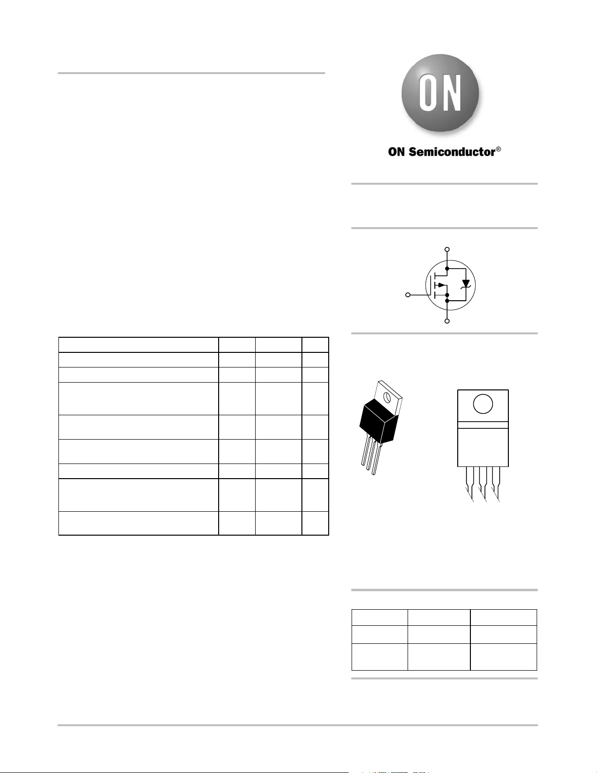
P−Channel TO−220
This Power MOSFET is designed for medium voltage, high speed
power switching applications such as switching regulators, converters,
solenoid and relay drivers.
Features
• Silicon Gate for Fast Switching Speeds − Switching Times Specified
at 100°C
• Designer’s Data − I
DSS
, V
DS(on)
, V
and SOA Specified
GS(th)
at Elevated Temperature
• Rugged − SOA is Power Dissipation Limited
• Source−to−Drain Diode Characterized for Use With Inductive Loads
• Pb−Free Package is Available*
MAXIMUM RATINGS (T
Rating
Drain−Source Voltage V
Drain−Gate Voltage (RGS = 1.0 MW)
Gate−Source Voltage
− Continuous
− Non−repetitive (t
Drain Current − Continuous
Drain Current − Pulsed
Total Power Dissipation
Derate above 25°C
Operating and Storage Temperature Range TJ, T
Thermal Resistance
− Junction−to−Case
− Junction−to−Ambient°
Maximum Lead Temperature for Soldering
Purposes, 1/8″ from case for 10 seconds
Stresses exceeding Maximum Ratings may damage the device. Maximum
Ratings are stress ratings only. Functional operation above the Recommended
Operating Conditions is not implied. Extended exposure to stresses above the
Recommended Operating Conditions may affect device reliability.
= 25°C unless otherwise noted)
C
Symbol Value Unit
DSS
V
DGR
V
GS
≤ 50 ms)
p
V
I
R
R
GSM
I
D
DM
P
D
q
JC
q
JA
T
L
stg
100 Vdc
100 Vdc
± 20
± 40
12
28
75
0.6
−6 5 to 150 °C
1.67
62.5
260 °C
Vdc
Vpk
Adc
W
W/°C
°C/W
http://onsemi.com
12 AMPERES, 100 VOLTS
R
DS(on)
G
4
TO−220AB
CASE 221A
1
2
3
MTP12P10 = Device Code
A = Location Code
Y = Year
WW = Work Week
G = Pb−Free Package
= 300 mW
P−Channel
D
S
MARKING DIAGRAM
AND PIN ASSIGNMEN
MTP12P10G
STYLE 5
1
Gate
Drain
AYWW
Drain
4
3
Source
2
*For additional information on our Pb−Free strategy and soldering details, please
download the ON Semiconductor Soldering and Mounting Techniques
Reference Manual, SOLDERRM/D.
© Semiconductor Components Industries, LLC, 2006
June, 2006 − Rev. 4
1 Publication Order Number:
ORDERING INFORMATION
Device Package Shipping
MTP12P10 TO−220AB 50 Units/Rail
MTP12P10G TO−220AB
(Pb−Free)
Preferred devices are recommended choices for future use
and best overall value.
50 Units/Rail
MTP12P10/D
Page 2
MTP12P10
)
ELECTRICAL CHARACTERISTICS (T
= 25°C unless otherwise noted)
J
Characteristic Symbol Min Max Unit
OFF CHARACTERISTICS
Drain−Source Breakdown Voltage (VGS = 0, ID = 0.25 mA) V
Zero Gate Voltage Drain Current
(VDS = Rated V
(VDS = Rated V
Gate−Body Leakage Current, Forward (V
Gate−Body Leakage Current, Reverse (V
, VGS = 0)
DSS
, VGS = 0, TJ = 125°C)
DSS
= 20 Vdc, VDS = 0) I
GSF
= 20 Vdc, VDS = 0) I
GSR
ON CHARACTERISTICS (Note 1)
Gate Threshold Voltage (V
T
= 100°C
J
= VGS, ID = 1.0 mA)
DS
Static Drain−Source On−Resistance (VGS = 10 Vdc, ID = 6.0 Adc) R
Drain−Source On−Voltage (VGS = 10 V)
(I
= 12 Adc)
D
(ID = 6.0 Adc, TJ = 100°C)
Forward Transconductance (VDS = 15 V, ID = 6.0 A) g
DYNAMIC CHARACTERISTICS
Input Capacitance
Output Capacitance C
(VDS = 25 V, VGS = 0, f = 1.0 MHz)
See Figure 10
Reverse Transfer Capacitance C
SWITCHING CHARACTERISTICS (Note 1) (TJ = 100°C)
Turn−On Delay Time
Rise Time t
Turn−Off Delay Time t
(VDD = 25 V, ID = 0.5 Rated ID, RG = 50 W)
See Figures 12 and 13
Fall Time t
Total Gate Charge
Gate−Source Charge Q
(VDS = 0.8 Rated V
, ID = Rated ID, VGS = 10 V
DSS
See Figure 11
Gate−Drain Charge Q
SOURCE−DRAIN DIODE CHARACTERISTICS (Note 1)
Forward On−Voltage
Forward Turn−On Time t
(IS = Rated ID, VGS = 0)
Reverse Recovery Time t
INTERNAL PACKAGE INDUCTANCE (TO−204)
Internal Drain Inductance, (Measured from the contact screw on the header closer to the
source pin and the center of the die)
Internal Source Inductance
(Measured from the source pin, 0.25″ from the package
to the source bond pad)
INTERNAL PACKAGE INDUCTANCE (TO−220)
Internal Drain Inductance
(Measured from the contact screw on tab to center of die)
(Measured from the drain lead 0.25″ from package to center of die)
Internal Source Inductance
(Measured from the source lead 0.25″ from package to source bond pad)
1. Pulse Test: Pulse Width ≤ 300 ms, Duty Cycle ≤ 2%.
(BR)DSS
I
DSS
GSSF
GSSR
V
GS(th)
DS(on)
V
DS(on)
FS
C
iss
oss
rss
t
d(on)
r
d(off)
f
Q
g
gs
gd
V
SD
on
rr
L
d
L
s
L
d
L
s
100 − Vdc
mAdc
−
−
10
100
− 100 nAdc
− 100 nAdc
2.0
1.5
− 0.3
4.5
4.0
Vdc
W
Vdc
−
−
4.2
3.8
2.0 − mhos
− 920 pF
− 575
− 200
− 50 ns
− 150
− 150
− 150
33 (Typ) 50 nC
16 (Typ) −
17 (Typ) −
4.0 (Typ) 5.5 Vdc
Limited by stray inductance
300
− ns
(Typ)
5.0 (Typ) −
12.5
−
nH
(Typ)
nH
3.5 (Typ)
4.5 (Typ)
−
−
7.5 (Typ) −
http://onsemi.com
2
Page 3
MTP12P10
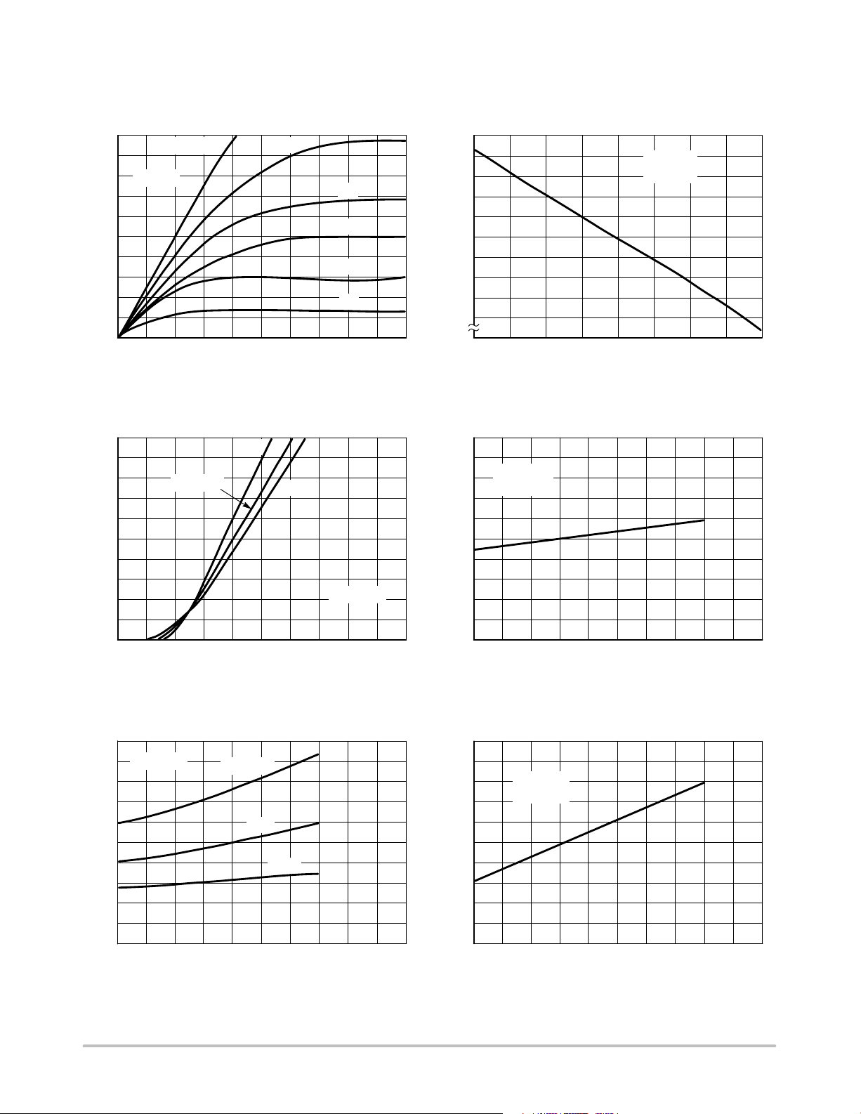
TYPICAL ELECTRICAL CHARACTERISTICS
20
18
16
14
12
10
8
6
, DRAIN CURRENT (AMPS)R
D
−I
4
2
0
VGS = −20 V
TJ = 25°C
−VDS, DRAIN−TO−SOURCE VOLTAGE (VOLTS)
10 V
8 V
7 V
6 V
5 V
109876543210
Figure 1. On−Region Characteristics
1.2
VDS = V
GS
1.1
1
0.9
0.8
, GATE THRESHOLD VOLTAGE (NORMALIZED)
GS(th)
−50 −25 0 25 50 75 100 125 150
V
TJ, JUNCTION TEMPERATURE (°C)
ID = 1 mA
Figure 2. Gate−Threshold Voltage Variation
With Temperature
20
16
12
TJ = −55°C
25°C
100°C
1.6
1.2
2
VGS = 0
I
= 0.25 mA
D
8
, DRAIN CURRENT (AMPS)
D
I
4
0
0.5
VGS = 15 V
0.4
0.3
0.2
0.1
, DRAIN−TO−SOURCE RESISTANCE (OHMS)
0
DS(on)
VDS = 20 V
VGS, GATE−TO−SOURCE VOLTAGE (VOLTS)
Figure 3. Transfer Characteristics
TJ = 100°C
25°C
−55°C
ID, DRAIN CURRENT (AMPS)
0.8
(NORMALIZED)
0.4
, DRAIN−TO−SOURCE BREAKDOWN VOLTAGE
201612840
0
−50 −75 0 25 50 75 100 125 150
BR(DSS)
V
TJ, JUNCTION TEMPERATURE (°C)
Figure 4. Normalized Breakdown Voltage
versus Temperature
1.8
1.6
1.4
1.2
1
0.8
(NORMALIZED)
0.6
, DRAIN−TO−SOURCE RESISTANCE
0.4
0.2
DS(on)
R
4036322824201612840
0
−50 −25 0 25 50 75 100 125 150
VGS = 10 V
I
= 6 A
D
TJ, JUNCTION TEMPERATURE (°C)
Figure 5. On−Resistance versus Drain Current
http://onsemi.com
Figure 6. On−Resistance Variation
With Temperature
3
Page 4

MTP12P10
SAFE OPERATING AREA INFORMATION
50
10 ms
0.1 ms
10
10 ms
1 ms
40
30
, DRAIN CURRENT (AMPS)
D
I
1
VGS = 20 V
SINGLE PULSE
TC = 25°C
R
LIMIT
DS(on)
PACKAGE LIMIT
THERMAL LIMIT
1
VDS, DRAIN−TO−SOURCE VOLTAGE (VOLTS)
dc
MTM/MTP12P06
MTM/MTP12P10
10
100
Figure 7. Maximum Rated Forward Biased
Safe Operating Area
FORWARD BIASED SAFE OPERATING AREA
The FBSOA curves define the maximum drain−to−source
voltage and drain current that a device can safely handle
when it is forward biased, or when it is on, or being turned
on. Because these curves include the limitations of
simultaneous high voltage and high current, up to the rating
of the device, they are especially useful to designers of linear
systems. The curves are based on a case temperature of 25°C
and a maximum junction temperature of 150°C. Limitations
for repetitive pulses at various case temperatures can be
determined by using the thermal response curves. ON
Semiconductor Application Note, AN569, “Transient
Thermal Resistance−General Data and Its Use” provides
detailed instructions.
20
, DRAIN CURRENT (AMPS)
D
I
10
0
02040 6080
MTM/MTP12P06
MTM/MTP12P10
10 30 50 70 90
VDS, DRAIN−TO−SOURCE VOLTAGE (VOLTS)
100
Figure 8. Maximum Rated Switching
Safe Operating Area
SWITCHING SAFE OPERATING AREA
The switching safe operating area (SOA) of Figure 8 is the
boundary that the load line may traverse without incurring
damage to the MOSFET. The fundamental limits are the
peak current, I
and the breakdown voltage, V
DM
(BR)DSS
The switching SOA shown in Figure 8 is applicable for both
turn−on and turn−off of the devices for switching times less
than one microsecond.
The power averaged over a complete switching cycle
must be less than:
T
− T
J(max)
C
R
q
JC
.
1
D = 0.5
0.5
0.3
0.2
0.2
0.1
0.1
0.05
0.05
0.02
0.03
r(t), NORMALIZED EFFECTIVE
0.02
TRANSIENT THERMAL RESISTANCE
0.01
0.01
SINGLE PULSE
0.02 0.05 0.1 0.2 0.5 1 2 5 10 20 50 100 200 500 1000
0.01
P
(pk)
t
1
t
2
DUTY CYCLE, D = t1/t
t, TIME (ms)
Figure 9. Thermal Response
http://onsemi.com
4
R
(t) = r(t) R
q
JC
R
q
JC
D CURVES APPLY FOR POWER
PULSE TRAIN SHOWN
READ TIME AT t
T
J(pk)
2
q
= 1.67°C/W MAX
− TC = P
JC
(pk)
1
R
(t)
q
JC
Page 5

MTP12P10
1600
1200
800
C, CAPACITANCE (pF)
400
0
PULSE GENERATOR
R
gen
C
iss
C
oss
C
rss
100
20
VDS, SOURCE−TO−DRAIN VOLTAGE (VOLTS)
Figure 10. Capacitance Variation
R
L
V
in
z = 50 W
50 W
50 W
TC = 25°C
V
= 0
GS
f = 1 MHz
−2
−4
−6
−8
−10
−12
, GATE SOURCE VOLTAGE (VOLTS)
GS
−14
V
4030
−16
RESISTIVE SWITCHING
V
DD
V
out
DUT
OUTPUT, V
INPUT, V
INVERTED
0
TJ = 25°C
= 12 A
I
D
VDS = 30 V
50 V
80 V
0 5 10 15 20 25 30 35 40 45 50
Q
, TOTAL GATE CHARGE (nC)
g
Figure 11. Gate Charge versus
Gate−To−Source Voltage
t
90%
off
90%90%
50%
t
f
t
in
d(on)
out
10%
t
on
50%
10%
t
r
PULSE WIDTH
t
d(off)
Figure 12. Switching Test Circuit
Figure 13. Switching Waveforms
http://onsemi.com
5
Page 6

MECHANICAL CASE OUTLINE
PACKAGE DIMENSIONS
SCALE 1:1
TO−220
CASE 221A−09
ISSUE AJ
DATE 05 NOV 2019
STYLE 1:
PIN 1. BASE
STYLE 5:
PIN 1. GATE
STYLE 9:
PIN 1. GATE
DOCUMENT NUMBER:
DESCRIPTION:
2. COLLECTOR
3. EMITTER
4. COLLECTOR
2. DRAIN
3. SOURCE
4. DRAIN
2. COLLECTOR
3. EMITTER
4. COLLECTOR
98ASB42148B
TO−220
STYLE 2:
PIN 1. BASE
2. EMITTER
3. COLLECTOR
4. EMITTER
STYLE 6:
PIN 1. ANODE
2. CATHODE
3. ANODE
4. CATHODE
STYLE 10:
PIN 1. GATE
2. SOURCE
3. DRAIN
4. SOURCE
STYLE 3:
PIN 1. CATHODE
2. ANODE
3. GATE
4. ANODE
STYLE 7:
PIN 1. CATHODE
2. ANODE
3. CATHODE
4. ANODE
STYLE 11:
PIN 1. DRAIN
2. SOURCE
3. GATE
4. SOURCE
Electronic versions are uncontrolled except when accessed directly from the Document Repository.
Printed versions are uncontrolled except when stamped “CONTROLLED COPY” in red.
STYLE 4:
PIN 1. MAIN TERMINAL 1
2. MAIN TERMINAL 2
3. GATE
4. MAIN TERMINAL 2
STYLE 8:
PIN 1. CATHODE
2. ANODE
3. EXTERNAL TRIP/DELAY
4. ANODE
STYLE 12:
PIN 1. MAIN TERMINAL 1
2. MAIN TERMINAL 2
3. GATE
4. NOT CONNECTED
PAGE 1 OF 1
ON Semiconductor and are trademarks of Semiconductor Components Industries, LLC dba ON Semiconductor or its subsidiaries in the United States and/or other countries.
ON Semiconductor reserves the right to make changes without further notice to any products herein. ON Semiconductor makes no warranty, representation or guarantee regarding
the suitability of its products for any particular purpose, nor does ON Semiconductor assume any liability arising out of the application or use of any product or circuit, and specifically
disclaims any and all liability, including without limitation special, consequential or incidental damages. ON Semiconductor does not convey any license under its patent rights nor the
rights of others.
© Semiconductor Components Industries, LLC, 2019
www.onsemi.com
Page 7

ON Semiconductor and are trademarks of Semiconductor Components Industries, LLC dba ON Semiconductor or its subsidiaries in the United States and/or other countries.
ON Semiconductor owns the rights to a number of patents, trademarks, copyrights, trade secrets, and other intellectual property. A listing of ON Semiconductor’s product/patent
coverage may be accessed at www.onsemi.com/site/pdf/Patent−Marking.pdf
ON Semiconductor makes no warranty, representation or guarantee regarding the suitability of its products for any particular purpose, nor does ON Semiconductor assume any liability
arising out of the application or use of any product or circuit, and specifically disclaims any and all liability, including without limitation special, consequential or incidental damages.
Buyer is responsible for its products and applications using ON Semiconductor products, including compliance with all laws, regulations and safety requirements or standards,
regardless of any support or applications information provided by ON Semiconductor. “Typical” parameters which may be provided in ON Semiconductor data sheets and/or
specifications can and do vary in different applications and actual performance may vary over time. All operating parameters, including “Typicals” must be validated for each customer
application by customer’s technical experts. ON Semiconductor does not convey any license under its patent rights nor the rights of others. ON Semiconductor products are not
designed, intended, or authorized for use as a critical component in life support systems or any FDA Class 3 medical devices or medical devices with a same or similar classification
in a foreign jurisdiction or any devices intended for implantation in the human body. Should Buyer purchase or use ON Semiconductor products for any such unintended or unauthorized
application, Buyer shall indemnify and hold ON Semiconductor and its officers, employees, subsidiaries, affiliates, and distributors harmless against all claims, costs, damages, and
expenses, and reasonable attorney fees arising out of, directly or indirectly, any claim of personal injury or death associated with such unintended or unauthorized use, even if such
claim alleges that ON Semiconductor was negligent regarding the design or manufacture of the part. ON Semiconductor is an Equal Opportunity/Affirmative Action Employer. This
literature is subject to all applicable copyright laws and is not for resale in any manner.
. ON Semiconductor reserves the right to make changes without further notice to any products herein.
PUBLICATION ORDERING INFORMATION
LITERATURE FULFILLMENT:
Email Requests to: orderlit@onsemi.com
ON Semiconductor Website: www.onsemi.com
TECHNICAL SUPPORT
North American Technical Support:
Voice Mail: 1 800−282−9855 Toll Free USA/Canada
Phone: 011 421 33 790 2910
Europe, Middle East and Africa Technical Support:
Phone: 00421 33 790 2910
For additional information, please contact your local Sales Representative
◊
www.onsemi.com
1
 Loading...