

Page 1
MT9V023
1/3-Inch Wide‐VGA CMOS
Digital Image Sensor
General Description
The ON Semiconductor MT9V023 is a 1/3-inch wide-VGA format
CMOS active-pixel digital image sensor with global shutter and high
dynamic range (HDR) operation. The sensor has specifically been
designed to support the demanding interior and exterior automotive
imaging needs, which makes this part ideal for a wide variety of
imaging applications in real-world environments.
This wide-VGA CMOS image sensor features ON Semiconductor’s
breakthrough low-noise CMOS imaging technology that achieves
CCD image quality (based on signal-to-noise ratio and low-light
sensitivity) while maintaining the inherent size, cost, and integration
advantages of CMOS.
The active imaging pixel array is 752 H x 480 V. It incorporates
sophisticated camera functions on-chip-such as binning 2 x 2 and
4 x 4, to improve sensitivity when operating in smaller resolutions-as
well as windowing, column and row mirroring. It is programmable
through a simple two-wire serial interface.
The MT9V023 can be operated in its default mode or be
programmed for frame size, exposure, gain setting, and other
parameters. The default mode outputs a wide-VGA-size image at 60
frames per second (fps).
An on-chip analog-to-digital converter (ADC) provides 10 bits per
pixel. A 12-bit resolution companded for 10 bits for small signals can
be alternatively enabled, allowing more accurate digitization for
darker areas in the image.
In addition to a traditional, parallel logic output the MT9V023 also
features a serial low-voltage differential signaling (LVDS) output. The
sensor can be operated in a stereo-camera, and the sensor, designated
as a stereo-master, is able to merge the data from itself and the
stereo-slave sensor into one serial LVDS stream.
The sensor is designed to operate in a wide temperature range
(–40°C to +105°C).
Features
• Array Format: Wide-VGA, Active 752 H x 480 V (360,960 pixels)
• Global Shutter Photodiode Pixels; Simultaneous Integration and
Readout
• Monochrome or Color: NIR Enhanced Performance for Use with
Non-visible NIR Illumination
• Readout Modes: Progressive or Interlaced
• Shutter Efficiency: >99%
• Simple Two-wire Serial Interface
• Real-time Exposure Context Switching - Dual Registerset
• Register Lock Capability
• Window Size: User Programmable to any Smaller Format (QVGA,
CIF, QCIF). Data Rate can be Maintained Independent of Window
Size
• Binning: 2 x 2 and 4 x 4 of the Full Resolution
www.onsemi.com
IBGA52 9x9
CASE 503AA
ORDERING INFORMATION
See detailed ordering and shipping information on page 2 of
this data sheet.
• ADC: On-chip, 10-bit Column-parallel
(Option to Operate in 12-bit to 10-bit
Companding Mode)
• Automatic Controls: Auto Exposure Control
(AEC) and Auto Gain Control (AGC);
Variable Regional and Variable Weight
AEC/AGC
• Support for Four Unique Serial Control
Register IDs to Control Multiple Imagers on
the Same Bus
• Data Output Formats:
• Single Sensor Mode:
10-bit Parallel/Stand-alone
8-bit or 10-bit Serial LVDS
• Stereo Sensor Mode:
Interspersed 8-bit Serial LVDS
• High Dynamic Range (HDR) Mode
Applications
• Automotive
• Unattended Surveillance
• Stereo Vision
• Smart Vision
• Automation
• Video as Input
• Machine Vision
© Semiconductor Components Industries, LLC, 2006
January, 2017 − Rev. 6
1 Publication Order Number:
MT9V023/D
Page 2

MT9V023
Table 1. KEY PERFORMANCE PARAMETERS
Parameter Value
Optical Format 1/3-inch
Active Imager Size 4.51 mm (H) x 2.88 mm (V)
Active Pixels 752 H x 480 V
Pixel Size 6.0 x 6.0 μm
Color Filter Array Monochrome or color RGB Bayer
Shutter Type Global Shutter
Maximum Data Rate
Master Clock
Full Resolution 752 x 480
Frame Rate 60 fps (at full resolution)
ADC Resolution 10-bit column-parallel
Responsivity 4.8 V/lux−sec (550 nm)
Dynamic Range >55 dB linear;
Supply Voltage 3.3 V ± 0.3 V (all supplies)
5.35 mm diagonal
pattern
27 Mp/s
27 MHz
>110 dB in HDR mode
Power Consumption <160 mW at maximum data rate
Operating Temperature –40°C to +105°C ambient
Packaging 52-ball IBGA, automotive-qualified;
(LVDS disabled); 120 μW standby
power
wafer or die
ORDERING INFORMATION
Table 2. AVAILABLE PART NUMBERS
Part Number
MT9V023IA7XTC−DP VGA 1/3” GS CIS Dry Pack with Protective Film
MT9V023IA7XTC−DR VGA 1/3” GS CIS Dry Pack without Protective Film
MT9V023IA7XTC−TP VGA 1/3” GS CIS Tape & Reel with Protective Film
MT9V023IA7XTC−TR VGA 1/3” GS CIS Tape & Reel without Protective Film
MT9V023IA7XTM−DR VGA 1/3” GS CIS Dry Pack without Protective Film
MT9V023IA7XTR−TP VGA 1/3” GS CIS Tape & Reel with Protective Film
Product Description Orderable Product Attribute Description
www.onsemi.com
2
Page 3
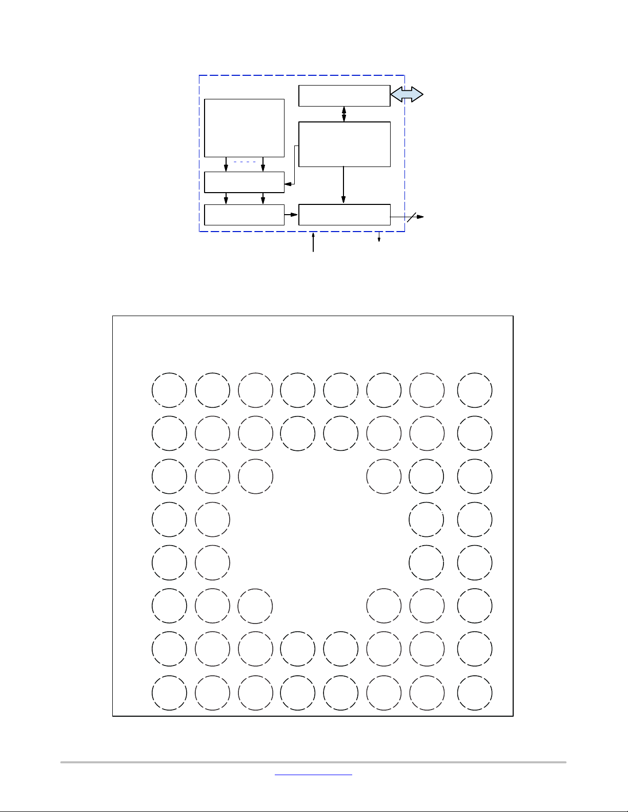
Active−Pixel
Sensor (APS)
Array
752H x 480V
Analog Processing
MT9V023
Control Register
Timing and Control
Serial
Register
I/O
A
B
C
1
VDD
LVDS
LVDS
GND
BYPASS
_CLKIN
_P
2
SER_
DATAOUT
_P
SHFT_
CLKOUT
_P
BYPASS
_CLKIN
_N
ADCs
Slave Video LVDS In
(for stereo applications only)
Figure 1. Block Diagram
3
SER_
DATAOUT
_N
SHFT_
CLKOUT
_N
LVDS
GND
4
VDD
LVDS
VDD
Digital Processing
Serial Video
LVDS Out
5
SYS−
DOUT0
CLK
PIXCLK
6
DOUT1
DGND
Parallel
Video
Data Out
7
DOUT2
DOUT4
AGND
8
DOUT3
VAAPIX
VAA
SER_
DATAIN
D
_P
DOUT5
E
DOUT6
F
DOUT8
G
DOUT9
H
SER_
DATAIN
_N
VDD
DOUT7
FRAME
_VALID
LINE_
VALID
DGND
STLN_
OUT
EXPO−
SURE
SDATA
SCLK
STFRM_
OUT
ERROR
AGND
LED_
OUT
OE
NC
NC
VAA
S_CTRL_
ADR0
RSVD
NC
NC
STAND−
BY
RESET_
BAR
S_CTRL
_ADR1
Figure 2. 52-Ball IBGA Package
www.onsemi.com
3
Page 4

MT9V023
BALL DESCRIPTIONS
Table 3. BALL DESCRIPTIONS
52-Ball IBA Numbers Symbol Type Description Note
H7 RSVD Input Connect to DGND. 1
D2 SER_DATAIN_N Input Serial data in for stereoscopy (differential negative).
D1 SER_DATAIN_P Input Serial data in for stereoscopy (differential positive).
C2 BYPASS_CLKIN_N Input Input bypass shift-CLK (differential negative). Tie to
C1 BYPASS_CLKIN_P Input Input bypass shift-CLK (differential positive). Tie to
H3 EXPOSURE Input Rising edge starts exposure in snapshot and slave
H4 SCLK Input Two-wire serial interface clock. Connect to VDD with
H6 OE Input DOUT enable pad, active HIGH. 2
G7 S_CTRL_ADR0 Input Two-wire serial interface slave address select (see
H8 S_CTRL_ADR1 Input Two-wire serial interface slave address select (see
G8 RESET_BAR Input Asynchronous reset. All registers assume defaults.
F8 STANDBY Input Shut down sensor operation for power saving.
A5 SYSCLK Input Master clock (26.6 MHz; 13 MHz – 27 MHz).
G4 SDATA I/O Two-wire serial interface data. Connect to VDD with
G3 STLN_OUT I/O
G5 STFRM_OUT I/O
H2 LINE_VALID Output Asserted when DOUT data is valid.
G2 FRAME_VALID Output Asserted when DOUT data is valid.
E1 DOUT5 Output Parallel pixel data output 5.
F1 DOUT6 Output Parallel pixel data output 6.
F2 DOUT7 Output Parallel pixel data output 7.
G1 DOUT8 Output Parallel pixel data output 8
H1 DOUT9 Output Parallel pixel data output 9.
H5 ERROR Output Error detected. Directly connected to STEREO
G6 LED_OUT Output LED strobe output.
B7 DOUT4 Output Parallel pixel data output 4.
A8 DOUT3 Output Parallel pixel data output 3.
A7 DOUT2 Output Parallel pixel data output 2.
B6 DOUT1 Output Parallel pixel data output 1.
A6 DOUT0 Output Parallel pixel data output 0.
Tie to 1KΩ pull-up (to 3.3 V) in non-stereoscopy
mode.
Tie to D
GND in non-stereoscopy mode.
1KΩ pull-up (to 3.3 V) in non-stereoscopy mode.
D
GND in non-stereoscopy mode.
modes.
1.5 K resistor even when no other two-wire serial
interface peripheral is attached.
Table 6).
Table 6).
1.5 K resistor even when no other two-wire serial
interface peripheral is attached.
Output in master mode−start line sync to drive slave
chip in-phase; input in slave mode.
Output in master mode−start frame sync to drive a
slave chip in-phase; input in slave mode.
ERROR FLAG.
www.onsemi.com
4
Page 5
MT9V023
Table 3. BALL DESCRIPTIONS (continued)
52-Ball IBA Numbers NoteDescriptionTypeSymbol
B5 PIXCLK Output Pixel clock out. DOUT is valid on rising edge of this
B3 SHFT_CLKOUT_N Output Output shift CLK (differential negative).
B2 SHFT_CLKOUT_P Output Output shift CLK (differential positive).
A3 SER_DATAOUT_N Output Serial data out (differential negative).
A2 SER_DATAOUT_P Output Serial data out (differential positive).
B4, E2 VDD Supply Digital power 3.3 V.
C8, F7 VAA Supply Analog power 3.3 V.
B8 VAAPIX Supply Pixel power 3.3 V.
A1, A4 VDDLVDS Supply Dedicated power for LVDS pads.
B1, C3 LVDSGND Ground Dedicated GND for LVDS pads.
C6, F3 DGND Ground Digital GND.
C7, F6 AGND Ground Analog GND.
E7, E8, D7, D8 NC NC No connect. 3
1. Pin H7 (RSVD) must be tied to GND.
2. Output enable (OE) tri-states signals D
OUT0–DOUT9, LINE_VALID, FRAME_VALID, and PIXCLK.
3. No connect. These pins must be left floating for proper operation.
clock.
1.5K
Ω
Master Clock
10K
Ω
DDLVDS
V
SYSCLK
OE
RESET_BAR
STANDBY from
Controller or
Digital GND
EXPOSURE
STANDBY
S_CTRL_ADR0
S_CTRL_ADR1
Two−Wire
Serial Interface
SCLK
DATA
S
RSVD
0.1 F
μ
Note: LVDS signals are to be left floating.
Figure 3. Typical Configuration (Connection) − Parallel Output Mode
VDD
VAA VAAPIX
VDD VAA
LVDSGND
VAAPIX
D
OUT(9:0)
LINE_VALID
FRAME_VALID
PIXCLK
LED_OUT
ERROR
A
GNDDGND
To Controller
To LED output
www.onsemi.com
5
Page 6
MT9V023
PIXEL DATA FORMAT
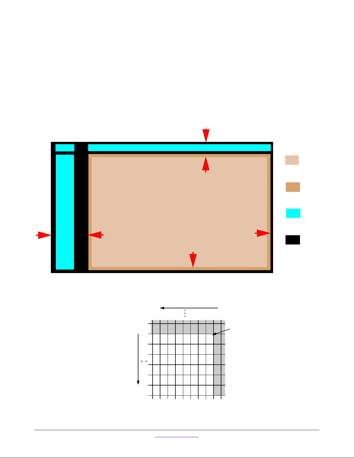
Pixel Array Structure
The MT9V023 pixel array is configured as 809 columns
by 499 rows, shown in Figure 4. The dark pixels are
optically black and are used internally to monitor black
level. Of the left 52 columns, 36 are dark pixels used for row
noise correction. Of the top 14 rows of pixels, two of the dark
rows are used for black level correction. Also, three black
rows from the top black rows can be read out by setting the
Show Dark Rows bit in the Read Mode register; setting
Show Dark Columns will display the 36 dark columns.
There are 753 columns by 481 rows of optically active
2 barrier + 8 (2 + 4 addressed + 2) dark + 2 barrier + 2 light dummy
pixels. While the sensor’s format is 752 x 480, one
additional active column and active row are included for use
when horizontal or vertical mirrored readout is enabled, to
allow readout to start on the same pixel. This one pixel
adjustment is always performed, for monochrome or color
versions. The active area is surrounded with optically
transparent dummy pixels to improve image uniformity
within the active area. Neither dummy pixels nor barrier
pixels can be read out.
(0, 0)
active pixel
4.92 x 3.05mm
Pixel Array
809 x 499 (753 x 481 active)
6.0 μm pixel
3 barrier + 38 (1 + 36 addressed + 1) dark
+ 9 barrier + 2 light dummy
2
2 barrier + 2 light dummy
Figure 4. Pixel Array Description
Column Readout Direction
Row Readout Direction
B
G
G
G
B
G
R
R
R
G
2 barrier + 2 light dummy
Active Pixel (0,0)
Array Pixel (4,14)
B
B
G
G
G
R
light dummy pixel
dark pixel
barrier pixel
B
G
G
B
G
R
R
G
B
G
G
B
G
R
R
G
G
G
G
G
R
R
B
B
G
G
G
G
R
R
B
B
Figure 5. Pixel Color Pattern Detail (Top Right Corner)
www.onsemi.com
6
Page 7

MT9V023
COLOR DEVICE LIMITATIONS
The color version of the MT9V023 does not support or
offers reduced performance for the following
functionalities.
Pixel Binning
Pixel binning is done on immediate neighbor pixels only,
no facility is provided to skip pixels according to a Bayer
pattern. Therefore, the result of binning combines pixels of
different colors. See “Pixel Binning” for additional
information.
Interlaced Readout
Interlaced readout yields one field consisting only of red
and green pixels and another consisting only of blue and
green pixels. This is due to the Bayer pattern of the CFA.
Automatic Black Level Calibration
When the color bit is set (R0x0F[1]=1), the sensor uses
black level correction values from one green plane, which
are applied to all colors. To use the calibration value based
on all dark pixels’ offset values, the color bit should be
cleared.
Defective Pixel Correction
For Defective Pixel Correction to calculate replacement
pixel values correctly, for color sensors the color bit must be
set (R0x0F[1] = 1). However, the color bit also applies
unequal offset to the color planes, and the results might not
be acceptable for some applications.
Other Limiting Factors
Black level correction and row-wise noise correction are
applied uniformly to each color. The row-wise noise
correction algorithm does not work well in color sensors.
Automatic exposure and gain control calculations are made
based on all three colors, not just the green channel. High
dynamic range does operate in color; however,
ON Semiconductor strongly recommends limiting use to
linear operation where good color fidelity is required.
www.onsemi.com
7
Page 8

MT9V023
OUTPUT DATA FORMAT
The MT9V023 image data can be read out in a progressive
scan or interlaced scan mode. Valid image data is surrounded
by horizontal and vertical blanking, as shown in Figure 6.
The amount of horizontal and vertical blanking is
programmable through R0x05 and R0x06, respectively
(R0xCD and R0xCE for context B). LV is HIGH during the
shaded region of the figure. See “Output Data Timing” for
the description of FV timing.
P
0,0 P0,1 P0,2
P
1,0 P1,1 P1,2
.....................................P
.....................................P
0,n−1P0,n
1,n−1P1,n
VALID IMAGE
P
m−1,0 Pm−1,1
P
m,0 Pm,1
.....................................P
.....................................P
m−1,n−1Pm−1,n
m,n−1Pm,n
00 00 00 ..................................... 00 00 00
00 00 00 ..................................... 00 00 00
VERTICAL BLANKING
00 00 00 ..................................... 00 00 00
00 00 00 ..................................... 00 00 00
00 00 00 .................. 00 00 00
00 00 00 .................. 00 00 00
HORIZONTAL
BLANKING
00 00 00 .................. 00 00 00
00 00 00 .................. 00 00 00
00 00 00 .................. 00 00 00
00 00 00 .................. 00 00 00
VERTICAL/HORIZONTAL
BLANKING
00 00 00 .................. 00 00 00
00 00 00 .................. 00 00 00
Figure 6. Spatial Illustration of Image Readout
www.onsemi.com
8
Page 9
MT9V023
OUTPUT DATA TIMING
The data output of the MT9V023 is synchronized with the
PIXCLK output. When LINE_VALID (LV) is HIGH, one
10-bit pixel datum is output every PIXCLK period.
LINE_VALID
PIXCLK
...
...
Valid Image DataBlanking Blanking
...
D
OUT(9:0)
P
0
(9:0)
P
(9:0)
1
(9:0)
Figure 7. Timing Example of Pixel Data
The PIXCLK is a nominally inverted version of the master
clock (SYSCLK). This allows PIXCLK to be used as a clock
to latch the data. However, when column bin 2 is enabled, the
PIXCLK is HIGH for one complete master clock master
period and then LOW for one complete master clock period;
when column bin 4 is enabled, the PIXCLK is HIGH for two
FRAME_VALID
LINE_VALID
Number of master clocks
Figure 8. Row Timing and FRAME_VALID/LINE_VALID Signals
Table 4. FRAME TIME
Parameters
A Active data time Context A: R0x04
P1 Frame start blanking Context A: R0x05 - 23
P2 Frame end blanking 23 (fixed) 23 pixel clocks
Q Horizontal blanking Context A: R0x05
A+Q Row time Context A: R0x04 + R0x05
V Vertical blanking Context A: (R0x06) x (A + Q) + 4
Name Equation
P1 A QA QAP2
Context B: R0xCC
Context B: R0xCD - 23
Context B: R0xCD
Context B: R0xCC + R0xCD
Context B: (R0xCE) x (A + Q) + 4
P2
P
3
(9:0)
P
4
(9:0)
...
P
n−1
(9:0)
P
n
(9:0)
complete master clock periods and then LOW for two
complete master clock periods. It is continuously enabled,
even during the blanking period. Setting R0x72 bit[4] = 1
causes the MT9V023 to invert the polarity of the PIXCLK.
The parameters P1, A, Q, and P2 in Figure 8 are defined
in Table 4.
...
...
...
Default Timing at
752 pixel clocks
= 752 master
= 28.2 μs
71 pixel clocks
= 71master
= 2.66 μs
= 23 master
= 0.86 μs
94 pixel clocks
= 94 master
= 3.52 μs
846 pixel clocks
= 846 master
= 31.72 μs
38,074 pixel clocks
= 38,074 master
= 1.43 ms
26.66 MHz
www.onsemi.com
9
Page 10

MT9V023
Table 4. FRAME TIME (continued)
Parameters
Nrows x (A + Q) Frame valid time Context A: (R0x03) × (A + Q)
Context B: (R0xCB) x (A + Q)
F Total frame time V + (Nrows x (A + Q)) 444,154 pixel clocks
Default Timing at
EquationName
26.66 MHz
406,080 pixel clocks
= 406,080 master
= 15.23 ms
= 444,154 master
= 16.66 ms
Sensor timing is shown above in terms of pixel clock and
master clock cycles (refer to Figure 7). The recommended
master clock frequency is 26.66 MHz. The vertical blanking
and the total frame time equations assume that the
integration time (Coarse Shutter Width plus Fine Shutter
Width) is less than the number of active rows plus the
blanking rows minus the overhead rows:
Table 5. In this example it is assumed that the Coarse Shutter
Width Control is programmed with 523 rows, and the Fine
Shutter Width Total is zero.
For Simultaneous mode, if the exposure time registers
(Coarse Shutter Width Total plus Fine Shutter Width Total)
exceed the total readout time, then the vertical blanking time
is internally extended automatically to adjust for the
additional integration time required. This extended value is
Window Height ) Vertical Blanking * 2
(eq.1)
not written back to the vertical blanking registers. The
Vertical Blank register can be used to adjust frame-to-frame
If this is not the case, the number of integration rows must
be used instead to determine the frame time, as shown in
Table 5. FRAME TIME−LONG INTEGRATION TIME
Parameter Name
V’
F’
1. The MT9V023 uses column parallel analog−digital converters, thus short row timing is not possible. The minimum total row time is 690
columns (horizontal width + horizontal blanking). The minimum horizontal blanking is 61. When the window width is set below 627, horizontal
blanking must be increased.
Vertical blanking (long integration time)
Total frame time (long integration time)
Context A:
(R0x0B + 2 − R0x03) y (A + Q) + R0xD5 + 4
Context B:
(R0xD2 + 2 − R0xCB) x (A + Q) + R0xD8 + 4
Context A: (R0x0B + 2) y (A + Q) + R0xD5 +4
Context B: (R0xD2 + 2) x (A + Q) + R0xD8 +4
readout time. This register does not affect the exposure time
but it may extend the readout time.
(Number of Master Clock Cycles)
Equation
Default Timing
at 26.66 MHz
38,074 pixel
clocks
= 38,074 master
= 1.43 ms
444,154 pixel
clocks
= 444,154 master
= 16.66 ms
www.onsemi.com
10
Page 11

MT9V023
SERIAL BUS DESCRIPTION
Registers are written to and read from the MT9V023
through the two-wire serial interface bus. The MT9V023 is
a serial interface slave with four possible IDs (0x90, 0x98,
0xB0 and 0xB8) determined by the S_CTRL_ADR0 and
S_CTRL_ADR1 input pins. Data is transferred into the
MT9V023 and out through the serial data (S
S
DATA line is pulled up to VDD off-chip by a 1.5KΩ resistor.
Either the slave or master device can pull the S
down−the serial interface protocol determines which device
is allowed to pull the S
DATA line down at any given time. The
registers are 16-bit wide, and can be accessed through 16−
or 8−bit two−wire serial interface sequences.
Protocol
The two-wire serial interface defines several different
transmission codes, as shown in the following sequence:
1. a start bit
2. the slave device 8-bit address
3. a(n) (no) acknowledge bit
4. an 8-bit message
5. a stop bit
Start Bit
The start bit is defined as a HIGH-to-LOW transition of
the data line while the clock line is HIGH.
Slave Address
The 8-bit address of a two-wire serial interface device
consists of 7 bits of address and 1 bit of direction. A “0” in
the LSB of the address indicates write mode, and a “1”
indicates read mode. As indicated above, the MT9V023
allows four possible slave addresses determined by the two
input pins, S_CTRL_ADR0 and S_CTRL_ADR1.
Acknowledge Bit
The master generates the acknowledge clock pulse. The
transmitter (which is the master when writing, or the slave
when reading) releases the data line, and the receiver
indicates an acknowledge bit by pulling the data line LOW
during the acknowledge clock pulse.
No-Acknowledge Bit
The no-acknowledge bit is generated when the data line is
not pulled down by the receiver during the acknowledge
clock pulse. A no-acknowledge bit is used to terminate a
read sequence.
DATA) line. The
DATA line
Stop Bit
The stop bit is defined as a LOW-to-HIGH transition of
the data line while the clock line is HIGH.
Sequence
A typical READ or WRITE sequence begins by the
master sending a start bit. After the start bit, the master sends
the slave device’s 8-bit address. The last bit of the address
determines if the request is a read or a write, where a “0”
indicates a WRITE and a “1” indicates a READ. The slave
device acknowledges its address by sending an
acknowledge bit back to the master.
If the request was a WRITE, the master then transfers the
8-bit register address to which a WRITE should take place.
The slave sends an acknowledge bit to indicate that the
register address has been received. The master then transfers
the data 8 bits at a time, with the slave sending an
acknowledge bit after each 8 bits. The MT9V023 uses 16-bit
data for its internal registers, thus requiring two 8-bit
transfers to write to one register. After 16 bits are transferred,
the register address is automatically incremented, so that the
next 16 bits are written to the next register address. The
master stops writing by sending a start or stop bit.
A typical READ sequence is executed as follows. First the
master sends the write mode slave address and 8-bit register
address, just as in the write request. The master then sends
a start bit and the read mode slave address. The master then
clocks out the register data 8 bits at a time. The master sends
an acknowledge bit after each 8-bit transfer. The register
address is automatically incremented after every 16 bits is
transferred. The data transfer is stopped when the master
sends a no-acknowledge bit. The MT9V023 allows for 8-bit
data transfers through the two-wire serial interface by
writing (or reading) the most significant 8 bits to the register
and then writing (or reading) the least significant 8 bits to
Byte-Wise Address register (0x0F0).
Bus Idle State
The bus is idle when both the data and clock lines are
HIGH. Control of the bus is initiated with a start bit, and the
bus is released with a stop bit. Only the master can generate
the start and stop bits.
www.onsemi.com
11
Page 12
MT9V023
Table 6. SLAVE ADDRESS MODES
{S_CTRL_ADR1, S_CTRL_ADR0} Slave Address Write/Read Mode
00
01
10
11
0x90 Write
0x91 Read
0x98 Write
0x99 Read
0xB0 Write
0xB1 Read
0xB8 Write
0xB9 Read
Data Bit Transfer
One data bit is transferred during each clock pulse. The
two-wire serial interface clock pulse is provided by the
master. The data must be stable during the HIGH period of
the serial clock−it can only change when the two-wire serial
interface clock is LOW. Data is transferred 8 bits at a time,
followed by an acknowledge bit.
www.onsemi.com
12
Page 13
MT9V023
P
TWO-WIRE SERIAL INTERFACE SAMPLE READ AND WRITE SEQUENCES
16-Bit Write Sequence
A typical write sequence for writing 16 bits to a register
is shown in Figure 9. A start bit given by the master,
followed by the write address, starts the sequence. The
image sensor then gives an acknowledge bit and expects the
register address to come first, followed by the 16-bit data.
After each 8-bit the image sensor gives an acknowledge bit.
SCLK
SDATA
All 16 bits must be written before the register is updated.
After 16 bits are transferred, the register address is
automatically incremented, so that the next 16 bits are
written to the next register. The master stops writing by
sending a start or stop bit.
0xBA ADDR
START ACK
Reg0x09
Figure 9. Timing Diagram Showing a WRITE to Reg0x09 with the Value 0x0284
16-Bit Read Sequence
A typical read sequence is shown in Figure 10. First the
master has to write the register address, as in a write
sequence. Then a start bit and the read address specifies that
a read is about to happen from the register. The master then
SCLK
DATA
S
0xBA ADDR 0xB9 ADDR 0000 0010
START ACK
Reg0x09
ACK ACK ACK
Figure 10. Timing Diagram Showing a READ from Reg0x09, Returned Value 0x0284
8-Bit Write Sequence
To be able to write 1 byte at a time to the register a special
register address is added. The 8-bit write is done by first
writing the upper 8 bits to the desired register and then
writing the lower 8 bits to the Bytewise Address register
0000 0010
ACK ACK ACK
1000 0100
clocks out the register data 8 bits at a time. The master sends
an acknowledge bit after each 8-bit transfer. The register
address is auto-incremented after every 16 bits is
transferred. The data transfer is stopped when the master
sends a no-acknowledge bit.
1000 0100
NACK
(R0xF0). The register is not updated until all 16 bits have
been written. It is not possible to just update half of a register.
In Figure 11, a typical sequence for 8-bit writing is shown.
The second byte is written to the Bytewise register (R0xF0).
STOP
STOP
CLK
ATA
0xB8 ADDR
Figure 11. Timing Diagram Showing a Bytewise Write to R0x09 with the Value 0x0284
R0x09
0000 0010 1000 0100
ACKSTART
0xB8 ADDR
START
www.onsemi.com
13
R0xF0
ACKACKACKACK
STO
ACK
Page 14

MT9V023
8-Bit Read Sequence
To read one byte at a time the same special register address
is used for the lower byte. The upper 8 bits are read from the
desired register. By following this with a read from the
SCLK
DATA
S
0xB8 ADDR 0000 0010
START
SCLK
SDATA
0xB8 ADDR 1000 0100
START
Figure 12. Timing Diagram Showing a Bytewise Read from R0x09; Returned Value 0x0284
R0x09
R0xF0
Bytewise Address register (R0xF0) the lower 8 bits are
accessed (Figure 12). The master sets the no-acknowledge
bits shown.
0xB9 ADDR
START
ACKACKACK
0xB9 ADDR
START
NACK
STOP
NACKACKACKACK
Register Lock
Included in the MT9V023 is a register lock (R0xFE)
feature that can be used as a solution to reduce the
probability of an inadvertent noise-triggered two-wire serial
interface write to the sensor. All registers, or only the Read
Mode registers–R0x0D and R0x0E, can be locked. It is
important to prevent an inadvertent two-wire serial interface
write to the Read Mode registers in automotive applications
since this register controls the image orientation and any
unintended flip to an image can cause serious results.
At power-up, the register lock defaults to a value of
0xBEEF, which implies that all registers are unlocked and
any two-wire serial interface writes to the register gets
committed.
Lock All Registers
If a unique pattern (0xDEAD) to R0xFE is programmed,
any subsequent two-wire serial interface writes to registers
(except R0xFE) are NOT committed. Alternatively, if the
user writes a 0xBEEF to the register lock register, all
registers are unlocked and any subsequent two-wire serial
interface writes to the register are committed.
Lock Only Read Mode Registers (R0x0D and R0x0E)
If a unique pattern (0xDEAF) to R0xFE is programmed,
any subsequent two-wire serial interface writes to R0x0D or
R0x0E are NOT committed. Alternatively, if the user writes
a 0xBEEF to register lock register, registers R0x0D and
R0x0E are unlocked and any subsequent two-wire serial
interface writes to these registers are committed.
www.onsemi.com
14
Page 15

MT9V023
Real-Time Context Switching
In the MT9V023, the user may switch between two full
register sets (listed in Table 7) by writing to a context switch
all registers (no shadowing) at the frame start time and have
the new values apply to the immediate next exposure and
readout time.
change bit in register 0x07. This context switch will change
Table 7. REAL-TIME CONTEXT−SWITCHABLE REGISTERS
Register Name Register Number (Hex) For Context A Register Number (Hex) for Context B
Column Start 0x01 0xC9
Row Start 0x02 0xCA
Window Height 0x03 0xCB
Window Width 0x04 0xCC
Horizontal Blanking 0x05 0xCD
Vertical Blanking 0x06 0xCE
Coarse Shutter Width 1 0x08 0xCF
Coarse Shutter Width 2 0x09 0xD0
Coarse Shutter Width Control 0x0A 0xD1
Coarse Shutter Width Total 0x0B 0xD2
Fine Shutter Width 1 0xD3 0xD6
Fine Shutter Width 2 0xD4 0xD7
Fine Shutter Width Total 0xD5 0xD8
Read Mode 0x0D [5:0] 0x0E [5:0]
High Dynamic Range enable 0x0F [0] 0x0F [8]
ADC Resolution Control 0x1C [1:0] 0x1C [9:8]
V1 Control – V4 Control 0x31 – 0x34 0x39 – 0x3C
Analog Gain Control 0x35 0x36
Row Noise Correction Control 1 0x70 [1:0] 0x70 [9:8]
Tiled Digital Gain 0x80 [3:0] – 0x98 [3:0] 0x80 [11:8] – 0x98 [11:8]
AEC/AGC Enable 0xAF [1:0] 0xAF [9:8]
www.onsemi.com
15
Page 16

MT9V023
FEATURE DESCRIPTION
Operational Modes
The MT9V023 works in master, snapshot, or slave mode.
In master mode the sensor generates the readout timing. In
snapshot mode it accepts an external trigger to start
integration, then generates the readout timing. In slave mode
the sensor accepts both external integration and readout
controls. The integration time is programmed through the
two-wire serial interface during master or snapshot modes,
or controlled through an externally generated control signal
during slave mode.
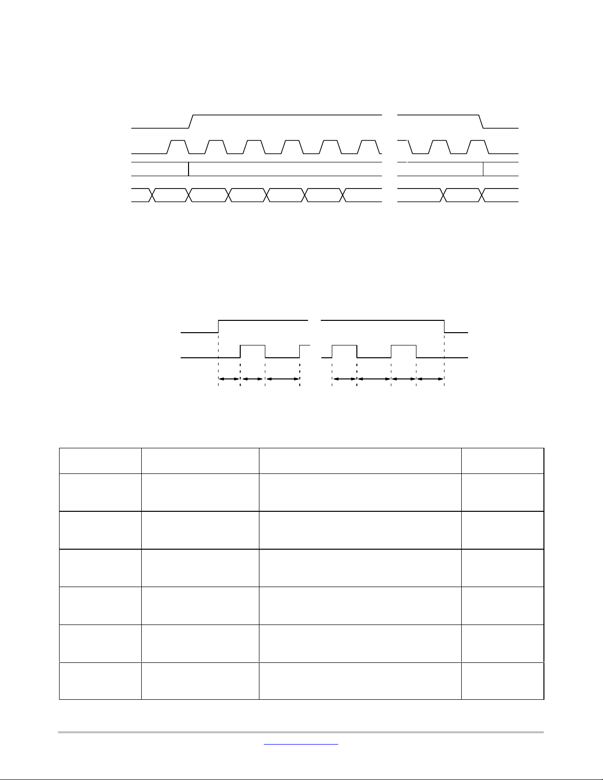
Master Mode
There are two possible operation methods for master
mode: simultaneous and sequential. One of these operation
modes must be selected through the two-wire serial
interface.
Readout Time > Exposure Time
Simultaneous Master Mode
In simultaneous master mode, the exposure period occurs
during readout. The frame synchronization waveforms are
shown in Figure 13 and Figure 14. The exposure and
readout happen in parallel rather than sequential, making
this the fastest mode of operation.
LED_OUT
FRAME_VALID
LINE_VALID
D
OUT(9:0)
LED_OUT
FRAME_VALID
LINE_VALID
OUT(9:0)
D
Exposure Time
Vertical Blanking
xxx xxx xxx
Figure 13. Simultaneous Master Mode Synchronization Waveforms #1
Exposure Time > Readout Time
Exposure Time
Vertical Blanking
xxx xxx xxx
Figure 14. Simultaneous Master Mode Synchronization Waveforms #2
When exposure time is greater than the sum of vertical
blank and window height, the number of vertical blank rows
www.onsemi.com
is increased automatically to accommodate the exposure
time.
16
Page 17

MT9V023
Sequential Master Mode
In sequential master mode the exposure period is followed
by readout. The frame synchronization waveforms for
LED_OUT
FRAME_VALID
LINE_VALID
OUT (9:0)
D
xxx xxx xxx
Figure 15. Sequential Master Mode Synchronization Waveforms
Snapshot Mode
In snapshot mode the sensor accepts an input trigger
signal which initiates exposure, and is immediately
followed by readout. Figure 16 shows the interface signals
used in snapshot mode. In snapshot mode, the start of the
integration period is determined by the externally applied
EXPOSURE pulse that is input to the MT9V023. The
integration time is preprogrammed at R0x0B or R0xD2
sequential master mode are shown in Figure 15. The frame
rate changes as the integration time changes.
Exposure Time
through the two-wire serial interface. After the frame’s
integration period is complete the readout process
commences and the syncs and data are output. Sensor in
snapshot mode can capture a single image or a sequence of
images. The frame rate may only be controlled by changing
the period of the user supplied EXPOSURE pulse train. The
frame synchronization waveforms for snapshot mode are
shown in Figure 17.
EXPOSURE
LED_OUT
FRAME_VALID
LINE_VALID
D
OUT(9:0)
EXPOSURE
SYSCLK
PIXCLK
CONTROLLER
LINE_VALID
FRAME_VALID
OUT
D
(9:0)
MT9V023
Figure 16. Snapshot Mode Interface Signals
Exposure Time
xxx xxx xxx
Figure 17.
Snapshot Mode Frame Synchronization Waveforms
www.onsemi.com
17
Page 18

MT9V023
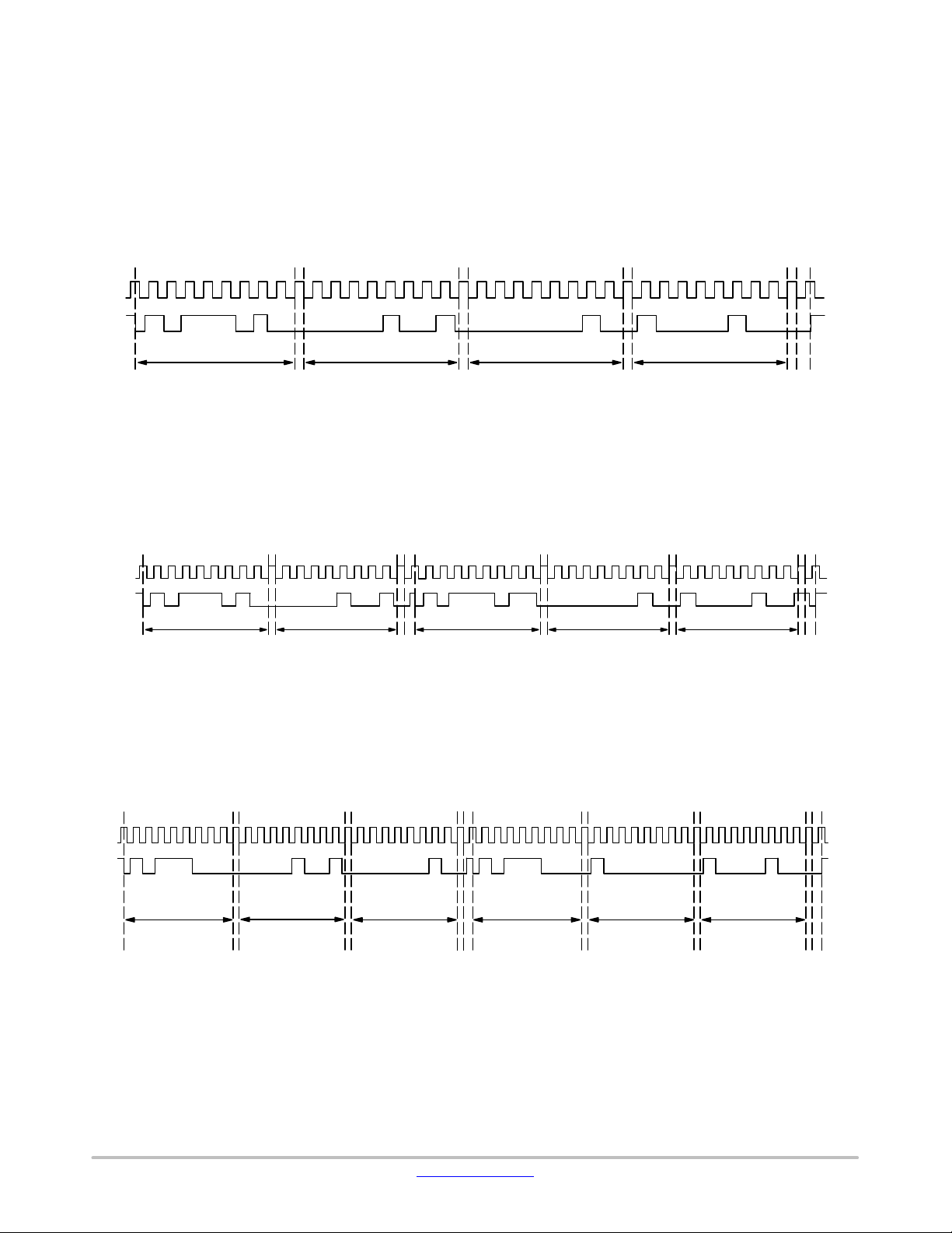
Slave Mode
In slave mode, the exposure and readout are controlled
using the EXPOSURE, STFRM_OUT, and STLN_OUT
pins. When the slave mode is enabled, STFRM_OUT and
STLN_OUT become input pins.
The start and end of integration are controlled by
EXPOSURE and STFRM_OUT pulses, respectively. While
a STFRM_OUT pulse is used to stop integration, it is also
used to enable the readout process.
After integration is stopped, the user provides
STLN_OUT pulses to trigger row readout. A full row of data
is read out with each STLN_OUT pulse. The user must
Exposure
(input)
STFRM_OUT
(input)
LED_OUT
(output)
STLN_OUT
(input)
LINE_VALID
(output)
Integration T ime
Figure 18. Slave Mode Operation
provide enough time between successive STLN_OUT
pulses to allow the complete readout of one row.
It is also important to provide additional STLN_OUT
pulses to allow the sensors to read the vertical blanking rows.
It is recommended that the user program the vertical blank
register (R0x06) with a value of 4, and achieve additional
vertical blanking between frames by delaying the
application of the STFRM_OUT pulse.
The elapsed time between the rising edge of STLN_OUT
and the first valid pixel data is calculated for context A by
[horizontal blanking register (R0x05) + 4] clock cycles. For
context B, the time is (R0xCD + 4) clock cycles.
Vertical Blanking
Signal Path
The MT9V023 signal path consists of a programmable
gain, a programmable analog offset, and a 10-bit ADC. See
Pixel Output
(reset minus signal)
Offset Correction
Voltage (R0x48 or
result of BLC)
C1
C2
Figure 19. Signal Path
“Black Level Calibration” for the programmable offset
operation description.
Gain Selection
(R0x35 or R0x36 or
result of AGC)
V
REF
(R0x2C)
10 (12) bit ADC
ADC Data
(9:0)
www.onsemi.com
18
Page 19

MT9V023
On-Chip Biases
ADC Voltage Reference
The ADC voltage reference is programmed through
R0x2C, bits 2:0. The ADC reference ranges from 1.0 V to
2.1 V. The default value is 1.4 V. The increment size of the
voltage reference is 0.1 \V from 1.0 V to 1.6 V (R0x2C[2:0]
values 0 to 6). At R0x2C[2:0] = 7, the reference voltage
jumps to 2.1 V.
It is very important to preserve the correct values of the
other bits in R0x2C. The default register setting is 0x0004.
This corresponds to 1.4 V−at this setting 1 mV input to the
ADC equals approximately 1 LSB.
V_Step Voltage Reference
This voltage is used for pixel high dynamic range
operations, programmable from R0x31 through R0x34 for
Context A, or R0x39 through R0x3B for context B.
Chip Version
Chip version register R0x00 is read-only.
Window Control
Registers Column Start A/B, Row Start A/B, Window
Height A/B (row size), and Window Width (column size)
A/B control the size and starting coordinates of the window.
The values programmed in the window height and width
registers are the exact window height and width out of the
sensor. The window start value should never be set below
four.
To read out the dark rows set bit 6 of R0x0D. In addition,
bit 7 of R0x0D can be used to display the dark columns in
the image. Note that there are Show Dark settings only for
Context A.
Blanking Control
Horizontal Blank and Vertical Blank registers R0x05 and
R0x06 (B: 0xCD and R0xCE), respectively, control the
blanking time in a row (horizontal blanking) and between
frames (vertical blanking).
• Horizontal blanking is specified in terms of pixel
clocks.
• Vertical blanking is specified in terms of numbers of
rows.
The actual imager timing can be calculated using Table 4
and Table 5 which describe “Row Timing and FV/LV
signals”.The minimum number of vertical blank rows is 4.
Pixel Integration Control
Total Integration
Total integration time is the result of coarse shutter width
and fine shutter width registers, and depends also on whether
manual or automatic exposure is selected.
The actual total integration time,
tt t
INT * INTCoarse ) INTFint
t
INT is defined as:
(eq. 2)
= (number of rows of integration x row time) + (number
of pixels of integration x pixel time)
where:
Number of Rows of Integration
(Auto Exposure Control: Enabled)
When automatic exposure control (AEC) is enabled, the
number of rows of integration may vary from frame to
frame, with the limits controlled by R0xAC (minimum
coarse shutter width) and R0xAD (maximum coarse shutter
width).
Number of Rows of Integration
(Auto Exposure Control: Disabled)
If AEC is disabled, the number of rows of integration
equals the value in R0x0B
or
If context B is enabled, the number of rows of integration
equals the value in R0xD2.
Number of Pixels of Integration
The number of fine shutter width pixels is independent of
AEC mode (enabled or disabled):
• Context A: the number of pixels of integration equals
the value in R0xD5.
• Context B: the number of pixels of integration equals
the value in R0xD8.
Row Timing
Context A : Row time + (R0x04 ) R0x05)
master clock periods
Context B : Row time + (R0xCC ) R0xCD)
master clock periods
Typically, the value of the Coarse Shutter Width Total
registers is limited to the number of rows per frame (which
includes vertical blanking rows), such that the frame rate is
not affected by the integration time. If the Coarse Shutter
Width Total is increased beyond the total number of rows per
frame, the user must add additional blanking rows using the
Vertical Blanking registers as needed. See descriptions of
the Vertical Blanking registers, R0x06 and R0xCE in Table
4 of the MT9V023 register reference.
A second constraint is that
t
INT must be adjusted to avoid
banding in the image from light flicker. Under 60 Hz flicker,
this means the frame time must be a multiple of 1/120 of a
second. Under 50 Hz flicker, the frame time must be a
multiple of 1/100 of a second.
Changes to Integration Time
With automatic exposure control disabled (R0xAF[0] for
context A, or R0xAF[8] for context B) and if the total
integration time (R0x0B or R0xD2) is changed through the
two-wire serial interface while FV is asserted for frame n,
the first frame output using the new integration time is frame
(eq. 3)
(eq. 4)
www.onsemi.com
19
Page 20

MT9V023
(n + 2). Similarly, when automatic exposure control is
enabled, any change to the integration time for frame n first
appears in frame (n + 2) output.
The sequence is as follows:
1. During frame n, the new integration time is held in
the R0x0B or R0D2 live register.
2. At the start of frame (n + 1), the new integration
time is transferred to the exposure control module.
Integration for each row of frame (n + 1) has been
completed using the old integration time. The
earliest time that a row can start integrating using
the new integration time is immediately after that
row has been read for frame (n + 1). The actual
time that rows start integrating using the new
FRAME_VALID
New Integration
Programmed
Actual
Integration
Int = 200 rows
Int = 200 rows
integration time is dependent on the new value of
the integration time.
3. When frame (n + 1) is read out, it is integrated
using the new integration time. If the integration
time is changed (R0x0B or R0xD2 written) on
successive frames, each value written is applied to
a single frame; the latency between writing a value
and it affecting the frame readout remains at two
frames. However, when automatic exposure
control is disabled, if the integration time is
changed through the two-wire serial interface after
the falling edge of FV for frame n, the first frame
output using the new integration time becomes
frame (n+3).
Int = 300 rows
Int = 300 rows
LED_OUT
Image Data
Frame Start
Figure 20. Latency When Changing Integration
Exposure Indicator
The exposure indicator is controlled by:
• R0x1B LED_OUT Control
The MT9V023 provides an output pin, LED_OUT, to
indicate when the exposure takes place. When R0x1B bit 0
Table 8. HIGH DYNAMIC RANGE
Context A Context B
High Dynamic Enable R0x0F[0] R0x0F[8]
Shutter Width 1 R0x08 R0xCF
Shutter Width 2 R0x09 R0xD0
Shutter Width Control R0x0A R0xD1
V_Step Voltages R0x31−R0x34 R0x39−R0x3C
Output image with
Int = 200 rows
Output
image with
Int = 300
rows
is clear, LED_OUT is HIGH during exposure. By using
R0x1B, bit 1, the polarity of the LED_OUT pin can be
inverted.
High Dynamic Range
High dynamic range is controlled by:
In the MT9V023, high dynamic range (by setting R0x0F,
bit 0 or 8 to 1) is achieved by controlling the saturation level
of the pixel (HDR or high dynamic range gate) during the
exposure period. The sequence of the control voltages at the
HDR gate is shown in Figure 21. After the pixels are reset,
the step voltage, V_Step, which is applied to HDR gate, is
www.onsemi.com
set up at V1 for integration time t
then V3 for time t
, and finally it is parked at V4, which also
3
then to V2 for time t2,
1,
serves as an antiblooming voltage for the photodetector.
This sequence of voltages leads to a piecewise linear pixel
response, illustrated (approximately) in Figure 21 and
Figure 22.
20
Page 21

AA (3.3V)
V
MT9V023
Exposure
V1~1.4V
HDR
Voltage
t
1
Figure 21. Sequence of Control Voltages at the HDR Gate
Output
dV1
1/t
1
1/t
2
Figure 22. Sequence of Voltages in a Piecewise Linear Pixel Response
The parameters of the step voltage V_Step which takes
values V1, V2, and V3 directly affect the position of the knee
points in Figure 22.
Light intensities work approximately as a reciprocal of the
partial exposure time. Typically,
t
2 shorter, and so on. Thus the range of light intensities is
t
1 is the longest exposure,
shortest for the first slope, providing the highest sensitivity.
The register settings for V_Step and partial exposures are:
• V1 = R0x31, bits 5:0 (Context B: R0x39, bits 5:0)
• V2 = R0x32, bits 5:0 (Context B: R0x3A, bits 5:0)
• V3 = R0x33, bits 5:0 (Context B: R0x3B, bits 5:0)
• V4 = R0x34, bits 5:0 (Context B: R0x3C, bits 5:0)
t
•
INT = t1 + t2 + t3
There are two ways to specify the knee points timing, the
first by manual setting and the second by automatic knee
point adjustment. Knee point auto adjust is controlled for
context A by R0x0A[8] (where default is ON), and for
context B by R0xD1[8] (where default is OFF).
When the knee point auto adjust enabler is enabled (set
HIGH), the MT9V023 calculates the knee points
automatically using the following equations:
t
ttt
1 + INT * 2 * 3
t
t
2 + INT x (1ń2)
t
t
2 + INT x (1ń2)
R0x0A[3:0] or R0xD1[3:0]
R0x0A[7:4] or R0xD1[7:4]
(eq. 5)
(eq. 6)
(eq. 7)
V2~1.2V V3~1.0V
V4~0.8V
t
2
t
3
dV3
dV2
Light Intensity
1/t
3
As a default for auto exposure, t2 is 1/16 of tINT, t3 is 1/64
t
of
INT.
When the auto adjust enabler is disabled (set LOW),
t
and
3 may be programmed
through the two-wire serial interface:
t
1 + Coarse SW1 (row * times) ) Fine SW1 (pixel * times)
t
2 + Coarse SW2 * Coarse SW1 ) Fine SW2 * Fine SW1
t
3 + Total Integration * 1 * 2
+ Coarse Total Shutter Width ) Fine Shutter Width Total * 1 * 2
tt
(eq. 8)
(eq. 9)
tt
(eq. 10)
For context A these become:
t
1 + R0x08 ) R0xD3
t
2 + R0x09 * ROx08 ) R0xD4 * R0xD3
ttt
3 + R0x0B ) R0xD4 * 1 * 2
(eq. 11)
(eq. 12)
(eq. 13)
For context B these are:
t
1 + R0xCF ) R0xD6
t
2 + R0xD0 * ROxCF ) R0xD7 * R0xD6
ttt
3 + R0xD2 ) R0xD8 * 1 * 2
(eq. 14)
(eq. 15)
(eq. 16)
t
1, t2,
www.onsemi.com
21
Page 22

MT9V023
In all cases above, the coarse component of total
integration time may be based on the result of AEC or values
in Reg0x0B and Reg0xD2, depending on the settings.
Similar to Fine Shutter Width Total registers, the user
must not set the Fine Shutter Width 1 or Fine Shutter Width
ADC Companding Mode
By default, ADC resolution of the sensor is 10-bit.
Additionally, a companding scheme of 12-bit into 10-bit is
enabled by the ADC Companding Mode register. This mode
allows higher ADC resolution, which means less
10-bit
Codes
1,024
768
512
2 to 1 Companding (256 128)
256
No companding (256 256)
2 register to exceed the row time (Horizontal Blanking +
Window Width). The absolute maximum value for the Fine
Shutter Width registers is 1774 master clocks.
quantization noise at low-light, and lower resolution at high
light, where good ADC quantization is not so critical
because of the high level of the photon’s shot noise.
8 to 1 Companding (2,048 256)
4 to 1 Companding (1,536 384)
12-bit
Codes
1,024512256
Figure 23. 12- to 10-Bit Companding Chart
Gain Settings
Changes to Gain Settings
When the digital gain settings (R0x80
–R0x98) are
changed, the gain is updated on the next frame start.
However, the latency for an analog gain change to take effect
depends on the automatic gain control.
FRAME_VALID
New Integration
Programmed
Actual
Gain
Image Data
Frame Start
Gain = 3.0X Gain = 3.5X
4,0962,048
If automatic gain control is enabled (R0xAF, bit 1 is set to
HIGH), the gain changed for frame n first appears in frame
(n + 1); if the automatic gain control is disabled, the gain
changed for frame n first appears in frame (n + 2).
Both analog and digital gain change regardless of whether
the integration time is also changed simultaneously. See the
“MT9V023 Developer Guide” for more details.
Gain = 3.0X Gain = 3.5X
Output image with
Gain = 3.0X
Output
image with
Gain = 3.5X
Figure 24. Latency of Analog Gain Change When AGC Is Disabled
Analog Gain
Analog gain is controlled by:
• R0x35 Global Gain context A
• R0x36 Global Gain context B
www.onsemi.com
22
Page 23

MT9V023
The formula for gain setting is:
Gain + Bits[6 : 0] 0.0625
(eq. 17)
The analog gain range supported in the MT9V023 is
1X
–4X with a step size of 6.25 percent. To control gain
manually with this register, the sensor must NOT be in AGC
mode. When adjusting the luminosity of an image, it is
recommended to alter exposure first and yield to gain
increases only when the exposure value has reached a
maximum limit.
• Analog gain = bits (6:0) x 0.0625 for values 16–31
• Analog gain = bits (6:0)/2 x 0.125 for values 32–64
For values 16–31: each LSB increases analog gain 0.0625
v/v. A value of 16 = 1X gain. Range: 1X to 1.9375X.
For values 32–64: each 2 LSB increases analog gain 0.125
v/v (that is, double the gain increase for 2 LSB). Range: 2X
to 4X. Odd values do not result in gain increases; the gain
increases by 0.125 for values 32, 34, 36, and so on.
Digital Gain
Digital gain is controlled by:
• R0x99−R0xA4 Tile Coordinates
• R0x80−R0x98 Tiled Digital Gain and Weight
In the MT9V023, the gain logic divides the image into 25
tiles, as shown in Figure 25. The size and gain of each tile
can be adjusted using the above digital gain control registers.
Separate tile gains can be assigned for context A and context
B.
Registers 0x99–0x9E and 0x9F–0xA4 represent the
coordinates X0/5–X5/5 and Y0/5–Y5/5 in Figure 25,
respectively.
Digital gains of registers 0x80–0x98 apply to their
corresponding tiles. The MT9V023 supports a digital gain
of 0.25–3.75X.
When binning is enabled, the tile offsets maintain their
absolute values; that is, tile coordinates do not scale with row
or column bin setting.
NOTE:
There is one exception, for the condition when
Column Bin 4 is enabled (R0x0D[3:2] or
R0x0E[3:2] = 2). For this case, the value for
Digital Tile Coordinate
X–direction must be doubled.
The formula for digital gain setting is:
Digital Gain + Bits[3 : 0] 0.25
(eq. 18)
X0/5 X1/5 X2/5 X3/5 X4/5 X5/5
Y0/5
x0_y0 x1_y0 x4_y0
Y1/5
x0_y1 x1_y1 x4_y1
Y2/5
x0_y2 x1_y2 x4_y2
Y3/5
x0_y3 x1_y3 x4_y3
Y4/5
x0_y4 x1_y4 x4_y4
Y5/5
Black Level Calibration
Black level calibration is controlled by:
• Frame Dark Average: R0x42
• Dark Average Thresholds: R0x46
• Black Level Calibration Control: R0x47
Figure 25. Tiled Sample
• Black Level Calibration Value: R0x48
• Black Level Calibration Value Step Size: R0x4C
The MT9V023 has automatic black level calibration
on-chip, and if enabled, its result may be used in the offset
correction shown in Figure 26.
www.onsemi.com
23
Page 24

MT9V023
Gain Selection
(R0x35 or R0x36 or
result of AGC)
VREF
(R0x2C)
Pixel Output
(reset minus signal)
Offset Correction
Voltage (R0x48 or
result of BLC)
Figure 26. Black Level Calibration Flow Chart
C1
C2
The automatic black level calibration measures the
average value of pixels from 2 dark rows (1 dark row if row
bin 4 is enabled) of the chip. (The pixels are averaged as if
they were light-sensitive and passed through the appropriate
gain.)
This row average is then digitally low-pass filtered over
many frames (R0x47, bits 7:5) to remove temporal noise and
random instabilities associated with this measurement.
Then, the new filtered average is compared to a minimum
acceptable level, low threshold, and a maximum acceptable
level, high threshold.
If the average is lower than the minimum acceptable level,
the offset correction voltage is increased by a programmable
offset LSB in R0x4C. (Default step size is 2 LSB Offset =
1 ADC LSB at analog gain = 1X.)
If it is above the maximum level, the offset correction
voltage is decreased by 2 LSB (default).
10 (12) bit ADC
ADC Data
(9:0)
To avoid oscillation of the black level from below to
above, the region the thresholds should be programmed so
the difference is at least two times the offset DAC step size.
In normal operation, the black level calibration
value/offset correction value is calculated at the beginning
of each frame and can be read through the two-wire serial
interface from R0x48. This register is an 8-bit signed two’s
complement value.
However, if R0x47, bit 0 is set to “1,” the calibration value
in R0x48 is used rather than the automatic black level
calculation result. This feature can be used in conjunction
with the “show dark rows” feature (R0x0D[6]) if using an
external black level calibration circuit.
The offset correction voltage is generated according to the
following formulas:
Offset Correction Voltage + (8 * bit signed twoȀs complement calibration value, –127 127) 0.5 mV
ADC input voltage + (Pixel Output Voltage ) Offset Correction Voltage) Analog Gain
Defective Pixel Correction
Defective pixel correction is intended to compensate for
defective pixels by replacing their value with a value based
on the surrounding pixels, making the defect less noticeable
to the human eye. The locations of defective pixels are
Row-wise Noise Correction
Row-wise noise correction is controlled by the following
registers:
• R0x70 Row Noise Control
• R0x72 Row Noise Constant
to (eq. 19)
stored in a ROM on chip during the manufacturing process;
the maximum number of defects stored is 32. There is no
provision for later augmenting the table of programmed
defects. In the defect correction block, bad pixels will be
substituted by either the average of its neighboring pixels, or
its nearest-neighbor pixel, depending on pixel location.
Defective Pixel Correction is enabled by R0x07[9]. By
default, correction is enabled, and pixels mapped in internal
ROM are replaced with corrected values. This might be
Row-wise noise cancellation is performed by calculating
a row average from a set of optically black pixels at the start
of each row and then applying each average to all the active
pixels of the row. Read Dark Columns register bit and Row
Noise Correction Enable register bit must both be set to
enable row-wise noise cancellation to be performed. The
behavior when Read Dark Columns register bit = 0 and Row
Noise Correction Enable register bit = 1 is undefined.
unacceptable to some applications, in which case pixel
correction should be disabled (R0x07[9] = 0).
www.onsemi.com
24
(eq. 20)
Page 25

MT9V023
The algorithm works as follows:
Logical columns 755-790 in the pixel array provide 36
optically black pixel values. Of the 36 values, two smallest
value and two largest values are discarded. The remaining
32 values are averaged by summing them and discarding the
5 LSB of the result. The 10-bit result is subtracted from each
pixel value on the row in turn. In addition, a positive constant
will be added (Reg0x71, bits 7:0). This constant should be
set to the dark level targeted by the black level algorithm plus
the noise expected on the measurements of the averaged
values from dark columns; it is meant to prevent clipping
from negative noise fluctuations.
Pixel value + ADC value – dark column average ) R0x71[9 : 0]
(eq. 21)
EXP. LPF
(R0xA8)
MAX. EXPOSURE (R0xBD)
MIN EXPOSURE (R0xAC)
DESIRED BIN
(desired luminance)
(R0xA5)
MAX. GAIN
(R0xAB)
16
CURRENT BIN
MIN GAIN
UNIT
(R0xBC)
(current luminance)
UNIT
Automatic Gain Control and Automatic Exposure
Control
that optimal auto settings of exposure and (analog) gain are
computed and updated every frame.
R0xAF. When AEC is disabled (R0xAF[0] = 0), the sensor
uses the manual exposure value in coarse and fine shutter
width registers. When AGC is disabled (R0xAF[1] = 0), the
sensor uses the manual gain value in R0x35 or R0x36. See
“Pixel Integration Control” and the MT9V023 Developer
Guide, for more information.
EXP. SKIP
(R0xA6)
AEC
HISTOGRAM
GENERATOR
UNIT
AGC
Note that this algorithm does not work in color sensor.
The integrated AEC/AGC unit is responsible for ensuring
AEC and AGC can be individually enabled or disabled by
Coarse Shutter
Width Total
AEC
OUTPUT
AGC OUTPUT
AEC ENABLE
(R0xAF[0 or 8])
To exposure
0
timing control
1
R0xBB
To analog
1
gain control
0
R0xBA
GAIN LPF
(R0xAB)
Figure 27. Controllable and Observable AEC/AGC Registers
GAIN SKIP
The exposure is measured in row-time by reading R0xBB.
The exposure range is 1 to 2047. The gain is measured in
gain-units by reading R0xBA. The gain range is 16 to 63
(unity gain = 16 gain-units; multiply by 1/16 to get the true
gain).
When AEC is enabled (R0xAF), the maximum auto
exposure value is limited by R0xBD; minimum auto
exposure is limited by AEC Minimum Exposure, R0xAC.
NOTE: AEC does not support sub-row timing;
calculated exposure values are rounded down to
the nearest row-time. For smoother response,
manual control is recommended for short
exposure times.
When AGC is enabled (R0xAF), the maximum auto gain
value is limited by R0xAB; minimum auto gain is fixed to
16 gain-units.
(R0xA9)
MANUAL GAIN
A or B
AGC ENABLE
(R0xAF[1 or 9])
The exposure control measures current scene luminosity
and desired output luminosity by accumulating a histogram
of pixel values while reading out a frame. All pixels are used,
whether in color or mono mode. The desired exposure and
gain are then calculated from this for subsequent frame.
When binning is enabled, tuning of the AEC may be
required. The histogram pixel count register, R0xB0, may be
adjusted to reflect reduced pixel count. Desired bin register,
R0xA5, may be adjusted as required.
Pixel Clock Speed
The pixel clock speed is same as the master clock
(SYSCLK) at 26.66 MHz by default. However, when
column binning 2 or 4 (R0x0D or R0x0E, bit 2 or 3) is
enabled, the pixel clock speed is reduced by half and
one-fourth of the master clock speed respectively. See “Read
www.onsemi.com
25
Page 26

MT9V023
Mode Options” and “Column Binning” for additional
information.
Hard Reset of Logic
The RC circuit for the MT9V023 uses a 10kΩ resistor and
a 0.1µF capacitor. The rise time for the RC circuit is 1µs
maximum.
Soft Reset of Logic
Soft reset of logic is controlled by:
• R0x0C Reset
Bit 0 is used to reset the digital logic of the sensor while
preserving the existing two-wire serial interface
configuration. Furthermore, by asserting the soft reset, the
sensor aborts the current frame it is processing and starts a
new frame. Bit 1 is a shadowed reset control register bit to
explicitly reset the automatic gain and exposure control
feature.
These two bits are self-resetting bits and also return to “0”
during two-wire serial interface reads.
STANDBY Control
The sensor goes into standby mode by setting STANDBY
to HIGH. Once the sensor detects that STANDBY is
asserted, it completes the current frame before disabling the
digital logic, internal clocks, and analog power enable
signal. To release the sensor out from the standby mode,
reset STANDBY back to LOW. The LVDS must be powered
to ensure that the device is in standby mode. See ”Appendix
A – Power-On Reset and Standby Timing” for more
information on standby.
The sensor goes into monitor mode when R0xD9[0] is set
to HIGH. In this mode, the sensor first captures a
programmable number of frames (R0xC0), then goes into a
sleep period for five minutes. The cycle of sleeping for five
minutes and waking up to capture a number of frames
continues until R0xD9[0] is cleared to return to normal
operation.
In some applications when monitor mode is enabled, the
purpose of capturing frames is to calibrate the gain and
exposure of the scene using automatic gain and exposure
control feature. This feature typically takes less than 10
frames to settle. In case a larger number of frames is needed,
the value of R0xC0 may be increased to capture more
frames.
During the sleep period, none of the analog circuitry and
a very small fraction of digital logic (including a five-minute
timer) is powered. The master clock (SYSCLK) is therefore
always required.
Read Mode Options
(Also see “Output Data Format” and “Output Data
Timing”).
Column Flip
By setting bit 5 of R0x0D or R0x0E the readout order of
the columns is reversed, as shown in Figure 28.
Row Flip
By setting bit 4 of R0x0D or R0x0E the readout order of
the rows is reversed, as shown in Figure 29.
Monitor Mode Control
Monitor mode is controlled by:
• R0xD9 Monitor Mode Enable
• R0xC0 Monitor Mode Image Capture Control
LINE_VALID
Normal readout
OUT(9:0)
D
Reverse readout
OUT(9:0)
D
Figure 28. Readout of Six Pixels in Normal and Column Flip Output Mode
P4,1
(9:0)
P4,n
(9:0)
P4,2
(9:0)
P4,n−1
(9:0)
P4,3
(9:0)
P4,n−2
(9:0)
P4,4
(9:0)
P4,n−3
(9:0)
P4,5
(9:0)
P4,n−4
(9:0)
P4,6
(9:0)
P4,n−5
(9:0)
www.onsemi.com
26
Page 27

LINE_VALID
MT9V023
Normal readout
OUT(9:0)
D
Reverse readout
D
OUT(9:0)
Row4
(9:0)
Row484
(9:0)
Row5
(9:0)
Row483
(9:0)
Figure 29. Readout of Six Rows in Normal and Row Flip Output Mode
Pixel Binning
In addition to windowing mode in which smaller
resolutions (CIF, QCIF) are obtained by selecting a smaller
window from the sensor array, the MT9V023 also provides
the ability to down-sample the entire image captured by the
pixel array using pixel binning.
There are two resolution options: binning 2 and binning
4, which reduce resolution by two or by four, respectively.
Row and column binning are separately selected. Image
mirroring options will work in conjunction with binning.
For column binning, either two or four columns are
combined by averaging to create the resulting column. For
row binning, the binning result value depends on the
difference in pixel values: for pixel signal differences of less
than 200 LSB’s, the result is the average of the pixel values.
For pixel differences of greater than 200 LSB’s, the result is
the value of the darker pixel value.
Binning operation increases SNR but decreases
resolution. Enabling row bin2 and row bin4 improves frame
Row6
(9:0)
Row482
(9:0)
Row7
(9:0)
Row481
(9:0)
Row8
7(9:0)
Row480
7(9:0)
Row9
(9:0)
Row479
(9:0)
rate by 2x and 4x respectively. Column binning does not
increase the frame rate.
Row Binning
By setting bit 0 or 1 of R0x0D or R0x0E, only half or
one-fourth of the row set is read out, as shown in Figure 30.
The number of rows read out is half or one-fourth of the
value set in R0x03. The row binning result depends on the
difference in pixel values: for pixel signal differences less
than 200 LSB’s, the result is the average of the pixel values.
For pixel differences of 200 LSB’s or more, the result is
the value of the darker pixel value.
Column Binning
For column binning, either two or four columns are
combined by averaging to create the result. In setting bit 2
or 3 of R0x0D or R0x0E, the pixel data rate is slowed down
by a factor of either two or four, respectively. This is due to
the overhead time in the digital pixel data processing chain.
As a result, the pixel clock speed is also reduced accordingly.
LINE_VALID
Normal readout
DOUT(9:0)
LINE_VALID
Row Bin 2 readout
DOUT(9:0)
LINE_VALID
Row Bin 4 readout
DOUT(9:0)
Figure 30. Readout of 8 Pixels in Normal and Row Bin Output Mode
Row4
(9:0)
Row4
(9:0)
Row4
(9:0)
Row5
(9:0)
Row6
(9:0)
Row8
(9:0)
Row6
(9:0)
Row8
(9:0)
Row7
(9:0)
Row10
(9:0)
Row8
(9:0)
Row9
(9:0)
Row10
(9:0)
Row11
(9:0)
www.onsemi.com
27
Page 28

LINE_VALID
Normal readout
DOUT(9:0)
PIXCLK
LINE_VALID
Column Bin 2 readout
DOUT(9:0)
PIXCLK
LINE_VALID
Column Bin 4 readout
DOUT(9:0)
PIXCLK
MT9V023
D1
(9:0)D2(9:0)D3(9:0)D4(9:0)D5(9:0)D6(9:0)D7(9:0)D8(9:0)
D12
(9:0)
D1234
(9:0)
D34
(9:0)
D56
(9:0)
D5678
(9:0)
D78
(9:0)
Figure 31. Readout of 8 Pixels in Normal and Column Bin Output Mode
Interlaced Readout
The MT9V023 has two interlaced readout options. By
setting R0x07[2:0] = 1, all the even-numbered rows are read
out first, followed by a number of programmable field
blanking rows (set by R0xBF[7:0]), then the odd-numbered
rows, and finally the vertical blanking rows. By setting
R0x07[2:0] = 2 only one field row is read out.
P
4,1 P4,2 P4,3
P
6,0 P6,1 P6,2
P
m−2,0 Pm−2,2
P
m,2 Pm,2
00 00 00 ..................................... 00 00 00
00 00 00 ..................................... 00 00 00
P
5,1 P5,2 P5,3
P
7,0 P7,1 P7,2
P
m−3,1 Pm−3,2
P
m,1 Pm,1
00 00 00 ............................................................................................. 00 00 00
00 00 00 ............................................................................................. 00 00 00
.....................................P
.....................................P
VALID IMAGE − Even Field
.....................................P
.....................................P
.....................................P
.....................................P
VALID IMAGE − Odd Field
.....................................P
.....................................P
VERTICAL BLANKING
Consequently, the number of rows read out is half what is
set in the window height register. The row start register
determines which field gets read out; if the row start register
is even, then the even field is read out; if row start address
is odd, then the odd field is read out.
4,n−1P4,n
6,n−1P6,n
m−2,n−2Pm−2,n
m,n−1Pm,n
5,n−1P5,n
7,n−1P7,n
m−3,n−1Pm−3,n
m,n−1Pm,n
00 00 00 .................. 00 00 00
00 00 00 .................. 00 00 00
HORIZONTAL
BLANKING
FIELD BLANKING
00 00 00 .................. 00 00 00
00 00 00 .................. 00 00 00
00 00 00 .................. 00 00 00
00 00 00 .................. 00 00 00
Figure 32. Spatial Illustration of Interlaced Image Readout
www.onsemi.com
28
Page 29

MT9V023
When interlaced mode is enabled, the total number of
blanking rows are determined by both Field Blanking
Field Blanking + R0xBF[7 : 0]
Vertical Blanking + R0x06[8 : 0] – R0xBF[7 : 0] (contextA) or R0xCE[8 : 0] – R0xBF[7 : 0] (contextB)
register (R0xBF) and Vertical Blanking register (R0x06 or
R0xCE). The followings are their equations.
(eq. 22)
(eq. 23)
with
minimum vertical blanking requirement + 4 (absolute minimum operate; see Vertical Blanking Registers description for VBlank minimums
for valid image output)
(eq. 24)
Similar to progressive scan, FV is logic LOW during the
valid image row only. Binning should not be used in
conjunction with interlaced mode.
www.onsemi.com
29
Page 30

MT9V023
LINE_VALID
By setting bit 2 and 3 of R0x72, the LV signal can get three
different output formats. The formats for reading out four
Default
FRAME_VALID
LINE_VALID
Continuously
FRAME_VALID
LINE_VALID
XOR
FRAME_VALID
LINE_VALID
Figure 33. Different LINE_VALID Formats
LVDS Serial (Stand-Alone/Stereo) Output
The LVDS interface allows for the streaming of sensor
data serially to a standard off-the-shelf deserializer up to
eight meters away from the sensor. The pixels (and controls)
are packeted−12-bit packets for stand-alone mode and
18-bit packets for stereoscopy mode. All serial signalling
(CLK and data) is LVDS. The LVDS serial output could
either be data from a single sensor (stand-alone) or
stream-merged data from two sensors (self and its
stereoscopic slave pair). The appendices describe in detail
the topologies for both stand-alone and stereoscopic modes.
There are two standard deserializers that can be used. One
for a stand-alone sensor stream and the other from a
stereoscopic stream. The deserializer attached to a
stand-alone sensor is able to reproduce the standard parallel
output (8-bit pixel data, LV, FV, and PIXCLK). The
deserializer attached to a stereoscopic sensor is able to
reproduce 8-bit pixel data from each sensor (with embedded
LV and FV) and pixel-clk. An additional (simple) piece of
logic is required to extract LV and FV from the 8-bit pixel
rows and two vertical blanking rows are shown in Figure 33.
In the last format, the LV signal is the XOR between the
continuous LV signal and the FV signal.
data. Irrespective of the mode (stereoscopy/stand-alone),
LV and FV are always embedded in the pixel data.
In stereoscopic mode, the two sensors run in lock-step,
implying all state machines are in the same state at any given
time. This is ensured by the sensor-pair getting their sys-clks
and sys-resets in the same instance. Configuration writes
through the two-wire serial interface are done in such a way
that both sensors can get their configuration updates at once.
The inter-sensor serial link is designed in such a way that
once the slave PLL locks and the data-dly, shft-clk-dly and
stream-latency-sel are configured, the master sensor streams
valid stereo content irrespective of any variation voltage
and/or temperature as long as it is within specification. The
configuration values of data-dly, shft-clk-dly and
stream-latency-sel are either predetermined from the
board-layout or can be empirically determined by reading
back the stereo-error flag. This flag is asserted when the two
sensor streams are not in sync when merged. The combo_reg
is used for out-of-sync diagnosis.
Internal
PIXCLK
Internal
Parallel
Data
Internal
Line_Valid
Internal
Frame_Valid
External
Serial
Data Out
P41
P42
P43
P44
P45
1023
01
P46
1023
P51
P41 P42 P46
P43
P44
P53
P45
P54 P55 P56P52
21
P51 P52
P53
P54
P55
P56 2
3
Figure 34. Serial Output Format for a 6x2 Frame
1. External pixel values of 0, 1, 2, 3, are reserved (they only convey control information). Any raw pixel of value 0, 1, 2 and 3 will be substituted
with 4.
2. The external pixel sequence 1023, 0, 1023 is a reserved sequence (conveys control information for legacy support of MT9V021 applications).
Any raw pixel sequence of 1023, 0, 1023 will be substituted with an output serial stream of 1023, 4, 1023.
www.onsemi.com
30
Page 31

MT9V023
LVDS Output Format
In stand-alone mode, the packet size is 12 bits (2 frame bits
and 10 payload bits); 10-bit pixels or 8-bit pixels can be
selected. In 8-bit pixel mode (R0xB6[0] = 0), the packet
consists of a start bit, 8-bit pixel data (with sync codes), the
line valid bit, the frame valid bit and the stop bit. For 10-bit
pixel mode (R0xB6[0] = 1), the packet consists of a start bit,
10-bit pixel data, and the stop bit.
Table 9. LVDS PACKET FORMAT IN STAND-ALONE MODE (Stereoscopy Mode Bit De-Asserted)
use_10-bit_pixels Bit De-Asserted
12-Bit Packet
Bit[0] 1’b1 (Start bit) 1’b1 (Start bit)
Bit[1] PixelData[2] PixelData[0]
Bit2] PixelData[3] PixelData[1]
Bit[3] PixelData[4] PixelData[2]
Bit4] PixelData[5] PixelData[3]
Bit[5] PixelData[6] PixelData[4]
Bit[6] PixelData[7] PixelData[5]
Bit[7] PixelData[8] PixelData[6]
Bit[8] PixelData[9] PixelData[7]
Bit[9] Line_Valid PixelData[8]
Bit[10] Frame_Valid PixelData[9]
Bit[11] 1’b0 (Stop bit) 1’b0 (Stop bit)
(8-Bit Mode)
use_10-bit_pixels Bit Asserted
(10-Bit Mode)
In stereoscopic mode, the packet size is 18 bits (2 frame
bits and 16 payload bits). The packet consists of a start bit,
the master pixel byte (with sync codes), the slave byte (with
sync codes), and the stop bit.)
Table 10. LVDS PACKET FORMAT IN STEREOSCOPY MODE (Stereoscopy Mode Bit Asserted)
18-bit Packet Function
Bit[0] 1’b1 (Start bit)
Bit[1] MasterSensorPixelData[2]
Bit[2] MasterSensorPixelData[3]
Bit[3] MasterSensorPixelData[4]
Bit[4] MasterSensorPixelData[5]
Bit[5] MasterSensorPixelData[6]
Bit[6] MasterSensorPixelData[7]
Bit[7] MasterSensorPixelData[8]
Bit[8] MasterSensorPixelData[9]
Bit[9] SlaveSensorPixelData[2]
Bit[10] SlaveSensorPixelData[3]
Bit[11] SlaveSensorPixelData[4]
Bit[12] SlaveSensorPixelData[5]
Bit[13] SlaveSensorPixelData[6]
Bit[14] SlaveSensorPixelData[7]
Bit[15] SlaveSensorPixelData[8]
Bit[16] SlaveSensorPixelData[9]
Bit[17] 1’b0 (Stop bit)
www.onsemi.com
31
Page 32

MT9V023
Table 11. RESERVED WORDS IN THE PIXEL DATA STREAM
Pixel Data Reserved Word Flag
0 Precedes frame valid assertion
1 Precedes line valid assertion
2 Succeeds line valid de-assertion
3 Succeeds frame valid de-assertion
When LVDS mode is enabled along with column binning
(bin 2 or bin 4, R0x0D[3:2], the packet size remains the same
but the serial pixel data stream repeats itself depending on
whether 2X or 4X binning is set:
• For bin 2, LVDS outputs double the expected data
(post-binning pixel 0,0 is output twice in sequence,
followed by pixel 0,1 twice, . . .).
• For bin 4, LVDS outputs 4 times the expected data
(pixel 0,0 is output 4 times in sequence followed by
pixel 0,1 times 4, . . .).
The receiving hardware will need to undersample the
output stream getting data either every 2 clocks (bin 2) or
every 4 (bin 4) clocks.
Table 12. SER_DATAOUT_* STATE
R0xB1[1]
LVDS power down
0 0 Active
0 1 Active
1 0 Z
1 1 Z
LVDS data power down
If the sensor provides a pixel whose value is 0,1, 2, or 3
(that is, the same as a reserved word) then the outgoing serial
pixel value is switched to 4.
LVDS Enable and Disable
The Table 12 and Table 13 further explain the state of the
LVDS output pins depending on LVDS control settings.
When the LVDS block is not used, it may be left powered
down to reduce power consumption.
R0xB3[4]
SER_DATAOUT_*
Table 13. SHFT_CLK_* STATE
R0xB1[1]
LVDS power down
0 0 Active
0 1 Z
1 0 Z
1 1 Z
1. ERROR pin: When sensor is not in stereo mode, ERROR pin is at LOW.
LVDS shift-clk power down
R0xB2[4]
SHFT_CLKOUT_*
www.onsemi.com
32
Page 33

LVDS Data Bus Timing
The LVDS bus timing waveforms and timing
specifications are shown in Table 14 and Figure 35.
Data Rise/Fall Time
(10% − 90%)
LVDS Data Output
(SER_DATAOUT_N/P)
LVDS Clock Output
(Shft_CLKOUT_N/P)
MT9V023
Data Setup Time
Data Hold Time
Clock Rise/Fall Time
(10% − 90%)
Clock Jitter
Figure 35. LVDS Timing
Table 14. LVDS AC TIMING SPECIFICATIONS
(V
= 3.3 V ±0.3 V; TJ = – 40°C to +105°C; output load = 100 Ω; frequency 27 MHz)
PWR
Parameter Minimum Typical Maximum Unit
LVDS clock rise time – 0.22 0.30 ns
LVDS clock fall time – 0.22 0.30 ns
LVDS data rise time – 0.28 0.30 ns
LVDS data fall time – 0.28 0.30 ns
LVDS data setup time 0.3 0.67 – ns
LVDS data hold time 0.1 1.34 – ns
LVDS clock jitter – 92 ps
www.onsemi.com
33
Page 34

MT9V023
ELECTRICAL SPECIFICATIONS
Table 15. DC ELECTRICAL CHARACTERISTICS OVER TEMPERATURE
(V
= 3.3 V ±0.3 V; TJ = – 40°C to +105°C; Output Load = 10 pF; Frequency 13 MHz to 27 MHz; LVDS off)
PWR
Symbol Definition Condition Min. Typ. Max. Unit
VIH Input HIGH voltage VPWR − 1.4 – V
VIL Input LOW voltage – 1.3 V
IIN Input leakage current No pull-up resistor;
V
IN = VPWR or VGND
VOH Output HIGH voltage IOH = –4.0 mA VPWR − 0.3 – – V
VOL Output LOW voltage IOL = 4.0 mA – – 0.3 V
IOH Output HIGH current VOH = VDD − 0.7 −11 – – mA
IOL Output LOW current VOL = 0.7 – – 11 mA
IPWRA Analog supply current Default settings – 12 20 mA
IPIX Pixel supply current Default settings – 1.1 3 mA
IPWRD Digital supply current Default settings,
ILVD S LVDS supply current Default settings with
IPWRA
Standby
IPWRD
Standby
Clock Off
IPWRD
Standby
Clock On
Analog standby supply current STDBY = VDD – 0.2 3
Digital standby supply current
with clock off
Digital standby supply current
with clock on
C
LOAD = 10 pF
LVDS on
STDBY = VDD,
CLKIN = 0 MHz
STDBY= VDD,
CLKIN = 27 MHz
−5 – 5
– 42 60 mA
– 13 16 mA
– 0.1 10
– 1 2 mA
A
A
A
Table 16. DC ELECTRICAL CHARACTERISTICS (V
Symbol Definition Condition Min. Typ. Max. Unit
LVDS Driver DC Specifications
OD| Output differential voltage
|V
|DVOD| Change in VOD between
VOS Output offset voltage 1.0 1.2 1.4 mV
DVOS Pixel array current – – 35 mV
IOS Digital supply current
IOZ Output current when driver is
LVDS Receiver DC Specifications
VIDTH+
Iin Input current – –
complementary output states
tri-state
Input differential
RLOAD = 100
| VGPD| < 925mV
= 3.3 V ±0.3 V; TA = Ambient = 25°C)
PWR
250 – 400 mV
– – 50 mV
+ 1%
–100 – 100 mV
±10
±1
mA
±20
A
A
www.onsemi.com
34
Page 35

MT9V023
Table 17. ABSOLUTE MAXIMUM RATINGS
Symbol Parameter Min. Max. Unit
VSUPPLY Power supply voltage
ISUPPLY Total power supply
IGND Total ground current – 200 mA
VIN DC input voltage –0.3 VDD + 0.3 V
VOUT DC output voltage –0.3 VDD + 0.3 V
1
TSTG
Stresses exceeding those listed in the Maximum Ratings table may damage the device. If any of these limits are exceeded, device functionality
should not be assumed, damage may occur and reliability may be affected.
1. This is a stress rating only, and functional operation of the device at these or any other conditions above those indicated in
(all supplies)
current
Storage temperature –50 +150 °C
the operational sections of this specification is not implied. Exposure to absolute maximum rating conditions for extended
periods may affect reliability.
Table 18. AE ELECTRICAL CHARACTERISTICS
(V
= 3.3 V ±0.3 V; TJ= –40°C to +105°C; Output Load = 10 pF)
PWR
Symbol Definition Condition Min. Typ. Max. Unit
SYSCLK Input clock frequency Note 1 13.0 26.6 27.0 MHz
Clock duty cycle 45.0 50.0 55.0 %
t
R
t
F
tPLHP SYSCLK to PIXCLK propagation delay
tPD PIXCLK to valid DOUT(9:0) propagation delay
tSD Data setup time 14 16 – ns
tHD Data hold time 14 16 –
tPFLR PIXCLK to LV propagation delay
tPFLF PIXCLK to FV propagation delay
Input clock rise time – 3 5 ns
Input clock fall time – 3 5 ns
–0.3 4.5 V
– 200 mA
CLOAD = 10pF
CLOAD = 10pF
CLOAD = 10pF
CLOAD = 10pF
4 6 8 ns
–3 0.6 3 ns
5 7 9 ns
5 7 9 ns
Propagation Delays for PIXCLK and Data Out Signals
The pixel clock is inverted and delayed relative to the
master clock. The relative delay from the master clock
(SYSCLK) rising edge to both the pixel clock (PIXCLK)
t
F
SYSCLK
t
PLHP
PIXCLK
t
PD
DOUT(9:0)
Figure 36. Propagation Delays for PIXCLK and Data Out Signals
t
SD
www.onsemi.com
falling edge and the data output transition is typically 7ns.
Note that the falling edge of the pixel clock occurs at
approximately the same time as the data output transitions.
See Table 18 for data setup and hold times.
t
R
t
HD
35
Page 36

MT9V023
Propagation Delays for FRAME_VALID and
LINE_VALID Signals
The LV and FV signals change on the same rising master
clock edge as the data output. The LV goes HIGH on the
same rising master clock edge as the output of the first valid
pixel’s data and returns LOW on the same master clock
t
PFLR
PIXCLK
FRAME_VALID
LINE_VALID
Figure 37. Propagation Delays for FRAME_VALID and LINE_VALID Signals
Two-Wire Serial Bus Timing
Detailed timing waveforms and parameters for the
two-wire serial interface bus are shown in Figure 38 and
Table 19.
SCLK
DATA
S
SCLK
t
SRTH
Write Start
t
SCLK
Write Address
Bit 7
t
SCHW
t
SDSW
Write Address
Bit 0
t
ASW
rising edge as the end of the output of the last valid pixel’s
data.
As shown in the “Output Data Timing”, FV goes HIGH
143 pixel clocks before the first LV goes HIGH. It returns
LOW 23 pixel clocks after the last LV goes LOW.
t
PFLF
PIXCLK
FRAME_VALID
LINE_VALID
tr_sdat tf_sdat
90%
10%
t
STPS
Register Value
Bit 0
t
ASR
ACK
t
AHW
tr_clk
90%
10%
t
AHR
Register Address
Bit 7
t
SHDR
tf_clk
t
SDSR
t
STPH
Stop
S
DATA
Read Start
Read Address
Bit 7
Read Address
Bit 0
ACK
Register Value
Bit 7
Figure 38. Two-wire Serial Bus Timing
www.onsemi.com
36
Register Value
Bit 0
Page 37

MT9V023
Table 19. TWO-WIRE SERIAL BUS TIMING PARAMETERS (Test Conditions: 25°C, 26.67 MHz, and 3.3 V)
Symbol
f
SCLK
Serial interface input clock
frequency
t
SCLK
Serial Input clock period 2.5 μsec
SCLK duty cycle 40 50 60 %
t
r_sclk
t
f_sclk
t
r_sdat SDATA rise time
t
f_sdat SDATA fall time
t
SRTS
t
SRTH
t
SDSW SDATA setup
t
SDHW SDATA hold
t
ASW
t
AHW
t
STPS
t
STPH
t
ASR
t
AHR
t
SDSR SDATA setup
t
SDHR SDATA hold
SCLK rise time 165 ns
SCLK fall time 6 ns
Start setup time WRITE/READ 148 150 167 ns
Start hold time WRITE/READ 36.9 36 37.6 ns
ACK setup time WRITE 146 146 148 ns
ACK hold time WRITE 98.9 107 144 ns
Stop setup time WRITE/READ 624 ns
Stop hold time WRITE/READ 1.61 ns
ACK setup time READ 192 228 229 ns
ACK hold time READ 247 284 287 ns
CIN_SI Serial interface input pin
capacitance
CLOAD_SD
RSD
SDATA max load capacitance
SDATA external pull-up resistor
Parameter Condition Min. Typ. Max. Unit
400 kHz
1.5 k pull-up
180 ns
9 ns
WRITE 0 5 12 ns
WRITE 1.3 36 37 ns
READ 654 655 690 ns
READ 560 595 596 ns
3.5 pF
15 pF
1.5 kΩ
www.onsemi.com
37
Page 38

MT9V023
Minimum Master Clock Cycles
In addition to the AC timing requirements described in
Table 16, the two-wire serial bus operation also requires
SCLK
DATA
S
Figure 39. Serial Host Interface Start Condition Timing
SCLK
DATA
S
Note: All timing are in units of master clock cycle.
certain minimum master clock cycles between transitions.
These are specified in Figures 39 through 44, in units of
master clock cycles.
4
4
4
4
Figure 40. Serial Host Interface Stop Condition Timing
4
SCLK
DATA
S
Note: S
4
DATA is driven by an off-chip transmitter.
Figure 41. Serial Host Interface Data Timing for Write
5
SCLK
DATA
S
Note: SDATA is pulled LOW by the sensor, or allowed to be pulled HIGH by a pull-up resistor off-chip.
Figure 42. Serial Host Interface Data Timing for Read
www.onsemi.com
38
Page 39

MT9V023
0
5
10
15
20
25
30
35
40
350 450 550 650 750 850 950 1050 1150
6
SCLK
Sensor pulls down
DATA pin
DATA
S
S
Figure 43. Acknowledge Signal Timing After an 8-Bit WRITE to the Sensor
7
SCLK
Sensor tri−states S
S
DATA
(turns off pull down)
Note: After a READ, the master receiver must pull down S
complete, the master must generate a “No Acknowledge” by leaving S
a start or stop bit may be used.
Figure 44. Acknowledge Signal Timing After an 8−Bit READ from the Sensor
3
6
DATA pin
DATA to acknowledge receipt of data bits. When read sequence is
DATA to float HIGH. On the following cycle,
Blue
Green (B)
Green (R)
Red
Quantum Efficiency (%)
Wavelength (nm)
Figure 45. Typical Quantum Efficiency − Color
www.onsemi.com
39
Page 40

Quantum Efficiency (%)
MT9V023
60
50
40
30
20
10
0
350 450 550 650 750 850 950 1050 1150
Wavelength (nm)
Figure 46. Typical Quantum Efficiency − Monochrome
www.onsemi.com
40
Page 41

MT9V023
APPENDIX A – POWER-ON RESET AND STANDBY TIMING
There are no constraints concerning the order in which the
various power supplies are applied; however, the MT9V023
requires reset in order operate properly at power-up. Refer
to Figure 47 for the power-up, reset, and standby sequences.
Power
up
DD, VDDLVDS,
V
AA,VAAPIX
V
RESET_BAR
STANDBY
SYSCLK
MIN 10 SYSCLK cycles
SCLK,SDATA
Two−Wire Serial I/F
DOUT[9:0]
DATA OUTPUT
Driven = 0
non−Low−Power
Active
MIN 20 SYSCLK cycles
Pre−Standby
Note 3
Does not
respond to
serial
interface
when
STANDBY = 1
Low−Power
Standby
MIN 10 SYSCLK cycles
D
OUT[9:0]
Wake
up
non−Low−Power
Active
MIN 10 SYSCLK cycles
Power
down
Notes:
1. All output signals are defined during initial power-up with RESET_BAR held LOW without SYSCLK being active. To properly
reset the rest of the sensor, during initial power-up, assert RESET_BAR (set to LOW state) for at least 750 ns after all power
supplies have stabilized and SYSCLK is active (being clocked). Driving RESET_BAR to LOW state does not put the part in
a low power state.
2. Before using two-wire serial interface, wait for 10 SYSCLK rising edges after RESET_BAR is de-asserted.
3. Once the sensor detects that STANDBY has been asserted, it completes the current frame readout before entering standby
mode. The user must supply enough SYSCLKs to allow a complete frame readout. See Table 4, “Frame Time,” for more
information.
4. In standby, all video data and synchronization output signals are High-Z.
5. In standby, the two-wire serial interface is not active.
Figure 47. Power-up, Reset, Clock and Standby Sequence
www.onsemi.com
41
Page 42

MECHANICAL CASE OUTLINE
PACKAGE DIMENSIONS
IBGA52 9x9
CASE 503AA
ISSUE B
DATE 27 FEB 2020
GENERIC
MARKING DIAGRAM*
XXXX = Specific Device Code
Y = Year
ZZZ = Lot Traceability
*This information is generic. Please refer to
device data sheet for actual part marking.
Pb−Free indicator, “G” or microdot “G”, may
or may not be present. Some products may
not follow the Generic Marking.
DOCUMENT NUMBER:
DESCRIPTION:
ON Semiconductor and are trademarks of Semiconductor Components Industries, LLC dba ON Semiconductor or its subsidiaries in the United States and/or other countries.
ON Semiconductor reserves the right to make changes without further notice to any products herein. ON Semiconductor makes no warranty, representation or guarantee regarding
the suitability of its products for any particular purpose, nor does ON Semiconductor assume any liability arising out of the application or use of any product or circuit, and specifically
disclaims any and all liability, including without limitation special, consequential or incidental damages. ON Semiconductor does not convey any license under its patent rights nor the
rights of others.
© Semiconductor Components Industries, LLC, 2018
98AON93388F
IBGA52 9x9
Electronic versions are uncontrolled except when accessed directly from the Document Repository.
Printed versions are uncontrolled except when stamped “CONTROLLED COPY” in red.
PAGE 1 OF 1
www.onsemi.com
Page 43

ON Semiconductor and are trademarks of Semiconductor Components Industries, LLC dba ON Semiconductor or its subsidiaries in the United States and/or other countries.
ON Semiconductor owns the rights to a number of patents, trademarks, copyrights, trade secrets, and other intellectual property. A listing of ON Semiconductor’s product/patent
coverage may be accessed at www.onsemi.com/site/pdf/Patent−Marking.pdf
ON Semiconductor makes no warranty, representation or guarantee regarding the suitability of its products for any particular purpose, nor does ON Semiconductor assume any liability
arising out of the application or use of any product or circuit, and specifically disclaims any and all liability, including without limitation special, consequential or incidental damages.
Buyer is responsible for its products and applications using ON Semiconductor products, including compliance with all laws, regulations and safety requirements or standards,
regardless of any support or applications information provided by ON Semiconductor. “Typical” parameters which may be provided in ON Semiconductor data sheets and/or
specifications can and do vary in different applications and actual performance may vary over time. All operating parameters, including “Typicals” must be validated for each customer
application by customer’s technical experts. ON Semiconductor does not convey any license under its patent rights nor the rights of others. ON Semiconductor products are not
designed, intended, or authorized for use as a critical component in life support systems or any FDA Class 3 medical devices or medical devices with a same or similar classification
in a foreign jurisdiction or any devices intended for implantation in the human body. Should Buyer purchase or use ON Semiconductor products for any such unintended or unauthorized
application, Buyer shall indemnify and hold ON Semiconductor and its officers, employees, subsidiaries, affiliates, and distributors harmless against all claims, costs, damages, and
expenses, and reasonable attorney fees arising out of, directly or indirectly, any claim of personal injury or death associated with such unintended or unauthorized use, even if such
claim alleges that ON Semiconductor was negligent regarding the design or manufacture of the part. ON Semiconductor is an Equal Opportunity/Affirmative Action Employer. This
literature is subject to all applicable copyright laws and is not for resale in any manner.
. ON Semiconductor reserves the right to make changes without further notice to any products herein.
PUBLICATION ORDERING INFORMATION
LITERATURE FULFILLMENT:
Email Requests to: orderlit@onsemi.com
ON Semiconductor Website: www.onsemi.com
TECHNICAL SUPPORT
North American Technical Support:
Voice Mail: 1 800−282−9855 Toll Free USA/Canada
Phone: 011 421 33 790 2910
Europe, Middle East and Africa Technical Support:
Phone: 00421 33 790 2910
For additional information, please contact your local Sales Representative
◊
www.onsemi.com
1
 Loading...