

查询MR2535LRL供应商
MR2535
Overvoltage
Transient Suppressors
Medium Current
Designed for applications requiring a low voltage rectifier with
reverse avalanche characteristics for use as reverse power transient
suppressors. Developed to suppress transients in the automotive
system, these devices operate in the forward mode as standard
rectifiers or reverse mode as power avalanche rectifier and will protect
electronic equipment from overvoltage conditions.
• Avalanche Voltage 24 to 32 Volts
• High Power Capability
• Economical
• Increased Capacity by Parallel Operation
http://onsemi.com
Mechanical Characteristics
• Case: Epoxy, Molded
• Weight: 2.5 Grams (Approximately)
• Finish: All External Surfaces Corrosion Resistant and Terminal
Leads are Readily Solderable
• Maximum Lead Temperature for Soldering Purposes:
350°C 3/8″ from Case for 10 Seconds at 5 lbs. Tension
• Polarity: Indicated by Diode Symbol or Cathode Band
• Marking: MR2535L
MAXIMUM RATINGS (T
Rating
DC Peak Repetitive Reverse Voltage
Working Peak Reverse Voltage
DC Blocking Voltage
Repetitive Peak Reverse Surge Current
(Time Constant = 10 ms, Duty Cycle
≤ 1%, TC = 25°C) (See Note 1)
Average Rectified Forward Current
(Single Phase, Resistive Load, 60 Hz,
TC = 125°C) (See Figure 4)
Non–Repetitive Peak Surge Current
Surge Supplied at Rated
Load Conditions
Halfwave, Single Phase
Operating and Storage Junction
T emperature Range
= 25°C unless otherwise noted)
J
Symbol Value Unit
V
RRM
V
RWM
V
R
I
RSM
I
O
I
FSM
TJ, T
stg
20 Volts
62 Amps
6.0 Amps
600 Amps
–65 to
+175
°C
L SUFFIX
CASE 194
STYLE 1
ORDERING INFORMATION
Device Package Shipping
MR2535L Axial–Lead
Button
MR2535LRL Axial–Lead
Button
1000/Box
800/Reel
Semiconductor Components Industries, LLC, 1999
September, 1999 – Rev. 3
1 Publication Order Number:
MR2535L/D
MR2535
THERMAL CHARACTERISTICS
Lead
Characteristic
Thermal Resistance, Junction to Lead @ Both Leads to Heat Sink,
Equal Length
Thermal Resistance Junction to Case R
*Typical
Length
1/4″
3/8″
1/2″
Symbol Max Unit
R
θJL
θJC
7.5
10
13
0.8* °C/W
°C/W
ELECTRICAL CHARACTERISTICS (T
Instantaneous Forward Voltage
Reverse Current (VR = 20 Vdc, TC = 25°C) I
Breakdown Voltage
Breakdown Voltage
Breakdown Voltage Temperature Coefficient V
Forward Voltage Temperature Coefficient @ IF = 10 mA V
(1) Pulse Test: Pulse Width ≤ 300 µs, Duty Cycle ≤ 2%.
*Typical
(1)
(1)
(1)
(IR = 100 mAdc, TC = 25°C) V
(IR = 90 Amp, TC = 150°C, PW = 80 µs) V
= 25°C unless otherwise noted)
J
Characteristic Symbol Min Max Unit
(iF = 100 Amps, TC = 25°C) v
F
R
(BR)
(BR)
(BR)TC
FTC
— 1.1 Volts
— 200 nAdc
24 32 Volts
— 40 Volts
— 0.096* %/°C
— 2* mV/°C
http://onsemi.com
2
MR2535
1000
100
10
1
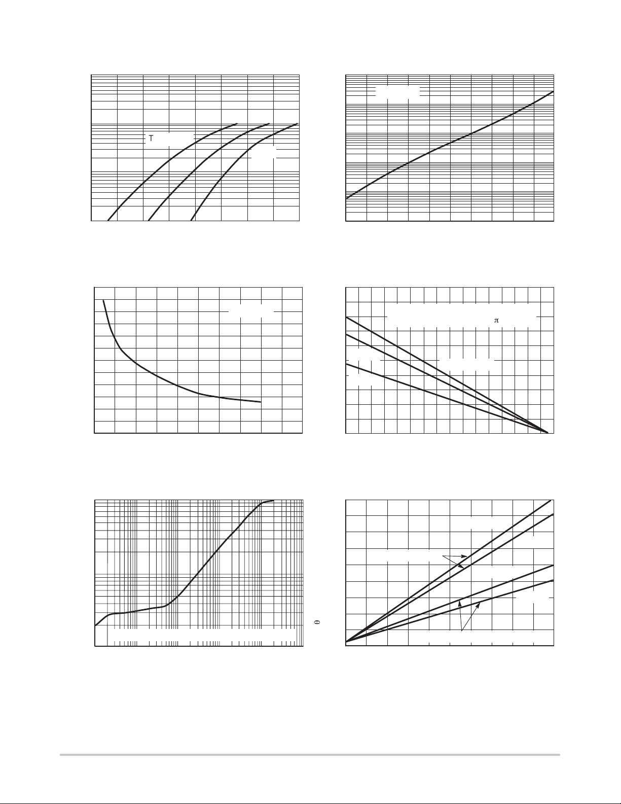
, INSTANTANEOUS FORWARD CURRENT (A)
F
I
4000
3500
3000
2500
2000
C, CAPACITANCE (pF)
1500
1000
VR = 20 V
100
75°C
0.1
, REVERSE CURRENT (nA)
R
I
0.01
10
1
TJ = 125°C
25°C
1000900800700600
VF, INSTANTANEOUS FORWARD VOLTAGE (mV) TJ, JUNCTION TEMPERATURE (°C)
Figure 1. T ypical Forward Voltage Figure 2. T ypical Reverse Current versus
Junction T emperature
25
TJ = 25°C
, AVERAGE FORWARD CURRENT (A)
20
15
10
10 mm
15 mm
5
Both leads to heatsink with equal length
I
F(peak)/IF(avg)
L = 6.25 mm
=
p
150125100755025
1000
Figure 3. T ypical Capacitance Figure 4. Maximum Current Ratings
1
0.1
r(t), TRANSIENT THERMAL
RESISTANCE (NORMALIZED)
0.01
L = 6.25 mm, both leads to heatsink (equal length)
2520151050
VR, DC BLOCKING VOLTAGE (V) TL, LEAD TEMPERATURE (°C)
45
40
35
30
25
20
15
, THERMAL RESIST ANCE
10
JL
q
JUNCTION TO LEAD ( C/W)°
R
5
0.1
t, TIME (S) LEAD LENGTH (mm)
1001010.010.001
0
Single to heatsink
Both leads to heatsink (equal length)
Maximum
Maximum
160
Typical
Typical
0
F(avg)
I
Figure 5. Thermal Response Figure 6. Steady State Thermal Resistance
18014012010080604020
2520151050
http://onsemi.com
3

MR2535
100
, PEAK REVERSE CURRENT (A)
RSM
I
1000
100
10000
TJ = 25°C
1000
, PEAK REVERSE POWER (W)
RSM
10
t, TIME CONSTANT (mS) t, TIME CONSTANT (mS)
P
1000100101
100
Figure 7. Maximum Peak Reverse Current Figure 8. Maximum Peak Reverse Power
2400
TJ = 25°C
2000
1600
1200
Time Constant = 10 mS
TJ = 25°C
1000100101
, PEAK REVERSE ENERGY (J)
RSM
W
10
800
400
PEAK REVERSE POWER (W)
1
1000100101
t, TIME CONSTANT (mS) TL, LEAD TEMPERATURE (°C)
0
Time Constant = 100 mS
125
150100755025
Figure 9. Maximum Reverse Energy Figure 10. Reverse Power Derating
1.20
1.18
1.16
1.14
1.12
1.10
/V
1.08
1.06
Z(Irsm) Z(100 mA)
V
1.04
1.02
1.00
I
RSM
PW = 80 mS, TL = 25°C
20 40
, REPETITIVE PEAK REVERSE SURGE CURRENT (A)
50
80 100
90 110
12070603010
Figure 11. Typical Clamping Factor
http://onsemi.com
4

MR2535
2 Ohms
dl/dt Limitation
100 mH
(%)
Figure 12. Load Dump T est Circuit
100
dl/dt < 1 A/ms
80
60
40
20
0
t (50%) t (10%)
t (37%)
Figure 13. Load Dump Pulse Current
50 mF0 – 150 V
t, TIME (S)
MR2535L
0.4
t (37%) = Time Constant
t (50%) = 0.7 t (37%)
t (10%) = 2.3 t (37%)
0.50.30.20.10
http://onsemi.com
5

Notes
MR2535
http://onsemi.com
6

MR2535
P ACKAGE DIMENSIONS
L SUFFIX
CASE 194–04
ISSUE F
A
NOTES:
D
1
K
B
K
2
1. CATHODE SYMBOL ON PACKAGE.
DIM MIN MAX MIN MAX
A 8.43 8.69 0.332 0.342
B 5.94 6.25 0.234 0.246
D 1.27 1.35 0.050 0.053
E 25.15 25.65 0.990 1.010
STYLE 1:
PIN 1. CATHODE
2. ANODE
INCHESMILLIMETERS
http://onsemi.com
7

MR2535
ON Semiconductor and are trademarks of Semiconductor Components Industries, LLC (SCILLC). SCILLC reserves the right to make changes
without further notice to any products herein. SCILLC makes no warranty , representation or guarantee regarding the suitability of its products for any particular
purpose, nor does SCILLC assume any liability arising out of the application or use of any product or circuit, and specifically disclaims any and all liability ,
including without limitation special, consequential or incidental damages. “Typical” parameters which may be provided in SCILLC data sheets and/or
specifications can and do vary in different applications and actual performance may vary over time. All operating parameters, including “Typicals” must be
validated for each customer application by customer’s technical experts. SCILLC does not convey any license under its patent rights nor the rights of others.
SCILLC products are not designed, intended, or authorized for use as components in systems intended for surgical implant into the body, or other applications
intended to support or sustain life, or for any other application in which the failure of the SCILLC product could create a situation where personal injury or
death may occur. Should Buyer purchase or use SCILLC products for any such unintended or unauthorized application, Buyer shall indemnify and hold
SCILLC and its officers, employees, subsidiaries, affiliates, and distributors harmless against all claims, costs, damages, and expenses, and reasonable
attorney fees arising out of, directly or indirectly , any claim of personal injury or death associated with such unintended or unauthorized use, even if such claim
alleges that SCILLC was negligent regarding the design or manufacture of the part. SCILLC is an Equal Opportunity/Affirmative Action Employer .
PUBLICATION ORDERING INFORMATION
USA/EUROPE Literature Fulfillment:
Literature Distribution Center for ON Semiconductor
P.O. Box 5163, Denver, Colorado 80217 USA
Phone: 303–675–2175 or 800–344–3860 Toll Free USA/Canada
Fax: 303–675–2176 or 800–344–3867 Toll Free USA/Canada
Email: ONlit@hibbertco.com
Fax Response Line*: 303–675–2167
800–344–3810 Toll Free USA/Canada
*To receive a Fax of our publications
N. America Technical Support: 800–282–9855 Toll Free USA/Canada
http://onsemi.com
ASIA/PACIFIC: LDC for ON Semiconductor – Asia Support
Phone: 303–675–2121 (Tue–Fri 9:00am to 1:00pm, Hong Kong Time)
Email: ONlit–asia@hibbertco.com
JAPAN: ON Semiconductor, Japan Customer Focus Center
4–32–1 Nishi–Gotanda, Shinagawa–ku, T okyo, Japan 141–8549
Phone: 81–3–5487–8345
Email: r14153@onsemi.com
ON Semiconductor Website: http://onsemi.com
For additional information, please contact your local Sales Representative.
MR2535L/D
8
 Loading...