

查询MPS2907ARLRA供应商
MPS2907A
Preferred Device
General Purpose
Transistors
PNP Silicon
MAXIMUM RATINGS
Rating Symbol Value Unit
Collector–Emitter Voltage V
Collector–Base Voltage V
Emitter–Base Voltage V
Collector Current – Continuous I
Total Device Dissipation
@ TA = 25°C
Derate above 25°C
Total Device Dissipation
@ TC = 25°C
Derate above 25°C
Operating and Storage Junction
Temperature Range
THERMAL CHARACTERISTICS
Characteristic Symbol Max Unit
Thermal Resistance,
Junction to Ambient
Thermal Resistance,
Junction to Case
CEO
CBO
EBO
P
P
TJ, T
R
θJA
R
θJC
http://onsemi.com
COLLECTOR
3
–60 Vdc
–60 Vdc
–5.0 Vdc
C
D
D
stg
–600 mAdc
625
5.0
1.5
12
–55 to
+150
200 °C/W
83.3 °C/W
mW
mW/°C
Watts
mW/°C
°C
2
BASE
EMITTER
STYLE 1
1
2
3
STYLES 1, 14
MARKING DIAGRAMS
MPS2
907A
YWW
Y = Year
WW = Work Week
1
TO–92
CASE 29
Semiconductor Components Industries, LLC, 2001
October, 2001 – Rev. 0
ORDERING INFORMATION
Device Package Shipping
MPS2907A TO–92 5000 Units/Box
MPS2907ARLRA TO–92 2000/Tape & Reel
MPS2907ARLRE TO–92 2000/Ammo Pack
MPS2907ARLRM TO–92 2000/Ammo Pack
MPS2907ARLRP TO–92 2000/Ammo Pack
Preferred devices are recommended choices for future use
and best overall value.
1 Publication Order Number:
MPS2907A/D
MPS2907A
CC C
CC C
ELECTRICAL CHARACTERISTICS (T
Characteristic Symbol Min Max Unit
= 25°C unless otherwise noted)
A
OFF CHARACTERISTICS
Collector–Emitter Breakdown Voltage (Note 1.)
(IC = –10 mAdc, IB = 0)
Collector–Base Breakdown Voltage
(IC = –10 Adc, IE = 0)
Emitter–Base Breakdown Voltage
(IE = –10 Adc, IC = 0)
Collector Cutoff Current
(VCE = –30 Vdc, V
Collector Cutoff Current
(VCB = –50 Vdc, IE = 0)
(VCB = –50 Vdc, IE = 0, TA = 150°C)
Base Current
(VCE = –30 Vdc, V
EB(off)
EB(off)
= –0.5 Vdc)
= –0.5 Vdc)
ON CHARACTERISTICS
DC Current Gain
(IC = –0.1 mAdc, VCE = –10 Vdc)
(IC = –1.0 mAdc, VCE = –10 Vdc)
(IC = –10 mAdc, VCE = –10 Vdc)
(IC = –150 mAdc, VCE = –10 Vdc) (Note 1.)
(IC = –500 mAdc, VCE = –10 Vdc) (Note 1.)
Collector–Emitter Saturation Voltage (Note 1.)
(IC = –150 mAdc, IB = –15 mAdc)
(IC = –500 mAdc, IB = –50 mAdc)
Base–Emitter Saturation Voltage (Note 1.)
(IC = –150 mAdc, IB = –15 mAdc)
(IC = –500 mAdc, IB = –50 mAdc)
SMALL–SIGNAL CHARACTERISTICS
Current–Gain – Bandwidth Product (Notes 1. and 2.),
(IC = –50 mAdc, VCE = –20 Vdc, f = 100 MHz)
Output Capacitance
(VCB = –10 Vdc, IE = 0, f = 1.0 MHz)
Input Capacitance
(VEB = –2.0 Vdc, IC = 0, f = 1.0 MHz)
SWITCHING CHARACTERISTICS
Turn–On T ime
Delay Time
Rise Time t
Turn–Off Time
Storage Time
Fall Time t
1. Pulse Test: Pulse Width 300 s, Duty Cycle 2%.
2. fT is defined as the frequency at which |hfe| extrapolates to unity.
(VCC = –30 Vdc, IC = –150 mAdc,
IB1 = –15 mAdc) (Figures 1 and 5)
(VCC = –6.0 Vdc, IC = –150 mAdc,
IB1 = IB2 = 15 mAdc) (Figure 2)
V
(BR)CEO
V
(BR)CBO
V
(BR)EBO
I
CEX
I
CBO
I
B
h
FE
V
CE(sat)
V
BE(sat)
f
T
C
obo
C
ibo
t
on
t
d
r
t
off
t
s
f
–60 –
–60 – Vdc
–5.0 – Vdc
– –50 nAdc
–
–
– –50 nAdc
75
100
100
100
50
–
–
–
–
200 – MHz
– 8.0 pF
– 30 pF
– 45 ns
– 10 ns
– 40 ns
– 100 ns
– 80 ns
– 30 ns
–0.01
–10
–
–
–
300
–
–0.4
–1.6
–1.3
–2.6
Vdc
µAdc
–
Vdc
Vdc
http://onsemi.com
2
MPS2907A
INPUT
Z
= 50 Ω
o
PRF = 150 PPS
RISE TIME ≤ 2.0 ns
P.W. < 200 ns
0
-16 V
200 ns
-30 V
200
1.0 k
50
TO OSCILLOSCOPE
RISE TIME ≤ 5.0 ns
INPUT
Z
= 50 Ω
o
PRF = 150 PPS
RISE TIME ≤ 2.0 ns
P.W. < 200 ns
0
-30 V
200 ns
+15 V -6.0 V
1.0 k
50
1.0 k 37
TO OSCILLOSCOPE
RISE TIME ≤ 5.0 ns
1N916
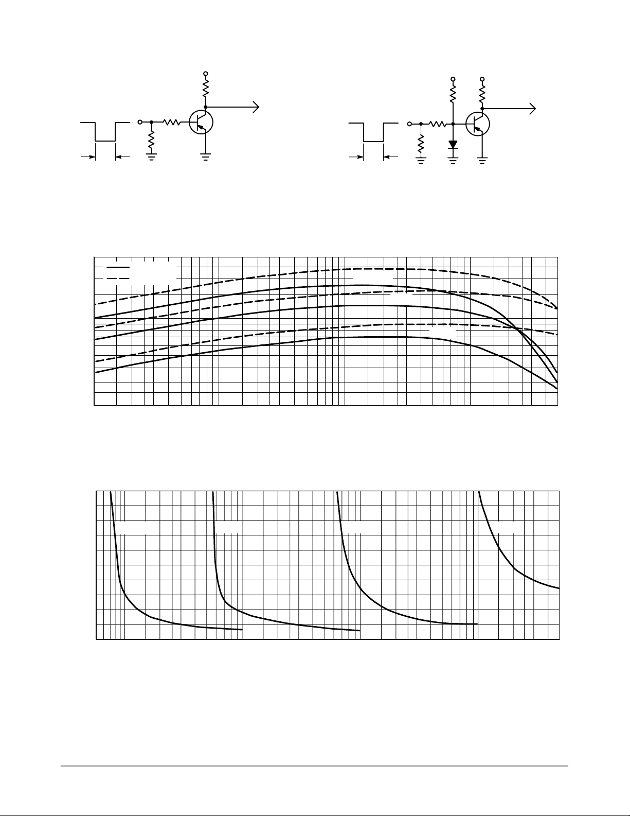
Figure 1. Delay and Rise Time Test Circuit Figure 2. Storage and Fall Time Test Circuit
TYPICAL CHARACTERISTICS
3.0
2.0
1.0
0.7
0.5
, NORMALIZED CURRENT GAIN
FE
0.3
h
VCE = -1.0 V
VCE = -10 V
T
= 125°C
J
25°C
-55°C
V , COLLECTOR-EMITTER VOLTAGE (VOLTS)
CE
0.2
-1.0
-0.8
-0.6
-0.4
-0.2
-0.005
-0.1
0
-0.2 -0.3 -0.5 -0.7 -1.0 -2.0 -3.0 -5.0 -7.0 -10 -20 -30 -50 -70 -100 -200 -300 -500
IC, COLLECTOR CURRENT (mA)
Figure 3. DC Current Gain
IC = -1.0 mA
-0.01
-10 mA
-0.02 -0.03 -0.05 -0.07 -0.1 -0.2 -0.3 -0.5 -0.7 -1.0
IB, BASE CURRENT (mA)
-100 mA
-2.0
-3.0
-5.0 -7.0 -10 -20
-500 mA
-30
Figure 4. Collector Saturation Region
-50
http://onsemi.com
3
 Loading...