

Page 1
© Semiconductor Components Industries, LLC, 2006
May, 2006 − Rev. 2
1 Publication Order Number:
MMT05B350T3/D
MMT05B350T3
Preferred Devices
Product Preview
Thyristor Surge Protectors
High Voltage Bidirectional TSPD
These Thyristor Surge Protective devices (TSPD) prevent
overvoltage damage to sensitive circuits by lightning, induction and
power line crossings. They are breakover−triggered crowbar
protectors. Turn−off occurs when the surge current falls below the
holding current value.
Secondary protection applications for electronic telecom equipment
at customer premises.
Features
• High Surge Current Capability: 50 A 10 x 1000 msec, for Controlled
Temperature Environments
• The MMT05B350T3 is used to help equipment meet various
regulatory requirements including: Bellcore 1089, ITU K.20 and
K.21, IEC 950, UL 1459 and 1950 and FCC Part 68
• Bidirectional Protection in a Single Device
• Little Change of Voltage Limit with Transient Amplitude or Rate
• Freedom from Wearout Mechanisms Present in Non−Semiconductor
Devices
• Fail−Safe, Shorts When Overstressed, Preventing Continued
Unprotected Operation
• Surface Mount Technology (SMT)
• Indicates UL Recognized − File #E210057
• Pb−Free Package is Available
MAXIMUM RATINGS (T
J
= 25°C unless otherwise noted)
Rating
Symbol Value Unit
Off−State Voltage − Maximum V
DM
300 V
Maximum Pulse Surge Short Circuit Current
Non−Repetitive Double Exponential Decay
Waveform (−25°C Initial Temperature)
(Notes 1 and 2)
2 x 10 msec
8 x 20 msec
10 x 160 msec
10 x 360 msec
10 x 560 msec
10 x 700 msec
10 x 1000 msec
I
PPS1
I
PPS2
I
PPS3
I
PPS4
I
PPS5
I
PPS6
I
PPS7
±150
±150
±100
±100
±70
±70
±50
A(pk)
Non−Repetitive Peak On−State Current
60 Hz Full Sign Wave
I
TSM
32 A(pk)
Maximum Non−Repetitive Rate of Change of
On−State Current Exponential Waveform, < 100 A
di/dt "300
A/ms
Stresses exceeding Maximum Ratings may damage the device. Maximum
Ratings are stress ratings only. Functional operation above the Recommended
Operating Conditions is not implied. Extended exposure to stresses above the
Recommended Operating Conditions may affect device reliability.
1. Allow cooling before testing second polarity.
2. Measured under pulse conditions to reduce heating.
This document contains information on a product under development. ON Semiconductor
reserves the right to change or discontinue this product without notice.
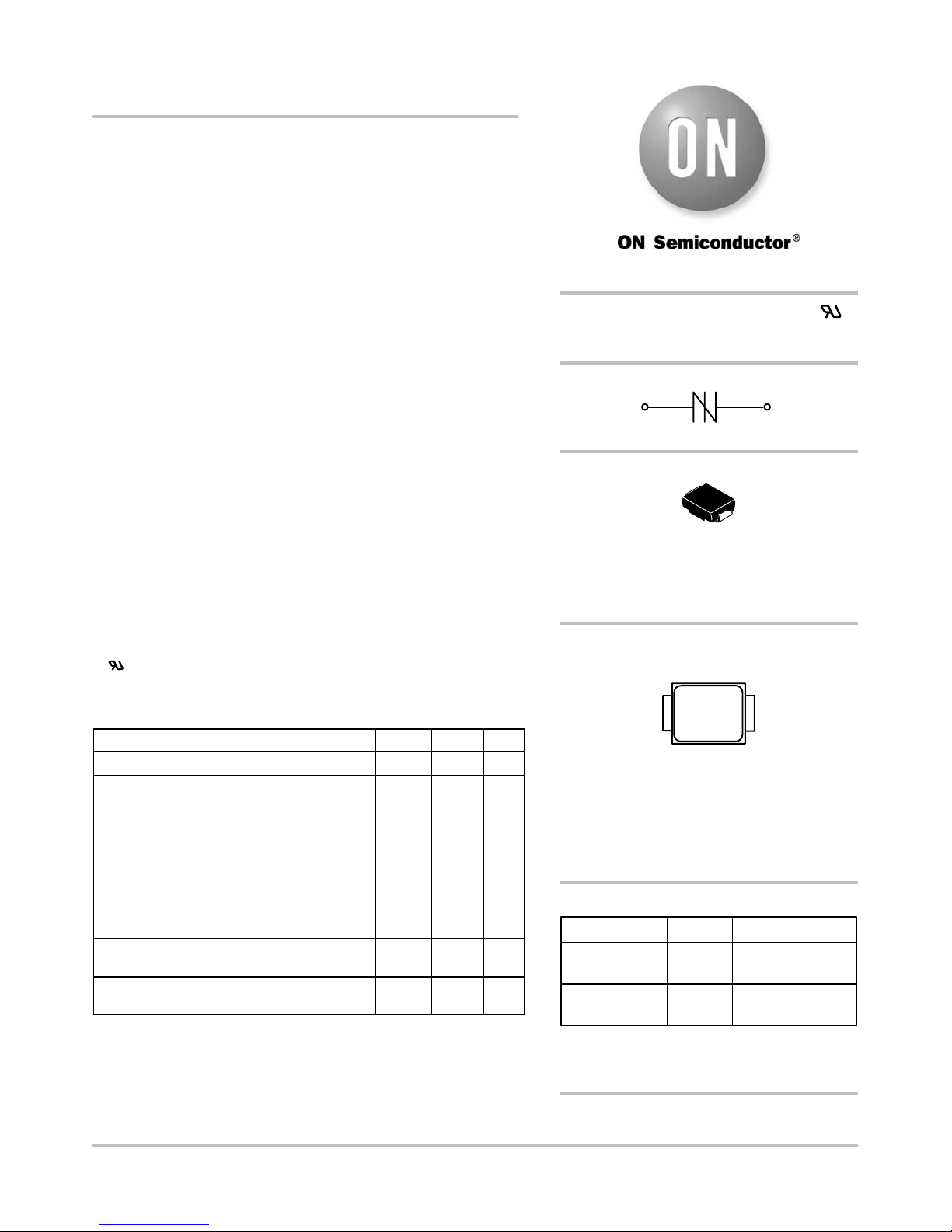
BIDIRECTIONAL TSPD
50 AMP SURGE, 350 VOLTS
Device Package Shipping
†
ORDERING INFORMATION
MMT05B350T3 SMB 12 mm Tape & Ree
l
(2.5 K/Reel)
MT1 MT2
SMB
(No Polarity)
(Essentially JEDEC DO−214AA)
CASE 403C
(
)
MARKING DIAGRAMS
http://onsemi.com
Preferred devices are recommended choices for future use
and best overall value.
†For information on tape and reel specifications,
including part orientation and tape sizes, please
refer to our Tape and Reel Packaging Specification
Brochure, BRD8011/D.
MMT05B350T3G SMB
(Pb−Free)
12 mm Tape & Ree
l
(2.5 K/Reel)
A = Assembly Location
Y = Year
WW = Work Week
RPBM = Specific Device Code
G = Pb−Free Package
(Note: Microdot may be in either location)
AYWW
RPBM G
G
Page 2
MMT05B350T3
http://onsemi.com
2
THERMAL CHARACTERISTICS
Characteristic Symbol Max Unit
Operating Temperature Range Blocking or Conducting State T
J1
−40 to +125 °C
Overload Junction Temperature − Maximum Conducting State Only T
J2
+175 °C
Maximum Lead Temperature for Soldering Purposes 1/8″ from Case for 10 Seconds T
L
260 °C
ELECTRICAL CHARACTERISTICS (T
J
= 25°C unless otherwise noted)
Devices are bidirectional. All electrical parameters apply to forward and reverse polarities.
Characteristics
Symbol Min Typ Max Unit
Breakover Voltage (Both polarities)
(dv/dt = 100 V/ms, I
SC
= 1.0 A, Vdc = 1000 V)
(+65°C)
V
(BO)
−
−
−
−
400
412
V
Breakover Voltage (Both polarities)
(f = 60 Hz, I
SC
= 1.0 A(rms), VOC = 1000 V(rms),
R
I
= 1.0 kW, t = 0.5 cycle) (Note 3)
(+65°C)
V
(BO)
−
−
−
−
400
412
V
Breakover Voltage Temperature Coefficient dV
(BO)
/dT
J
− 0.12 − V/°C
Breakdown Voltage (I
(BR)
= 1.0 mA) Both polarities V
(BR)
− 350 − V
Off State Current (VD1 = 50 V) Both polarities
Off State Current (V
D2
= VDM) Both polarities
I
D1
I
D2
−
−
−
−
2.0
5.0
mA
On−State Voltage (IT = 1.0 A)
(PW ≤ 300 ms, Duty Cycle ≤ 2%) (Note 3)
V
T
− 1.6 3.0 V
Breakover Current (f = 60 Hz, VDM = 1000 V(rms), RS = 1.0 kW)
Both polarities
I
BO
− 475 − mA
Holding Current (Both polarities) (Note 3)
V
S
= 500 V; IT (Initiating Current) = "1.0 A (+65°C)
I
H
150
130
270
−
−
−
mA
Critical Rate of Rise of Off−State Voltage
(Linear waveform, V
D
= Rated VBR, TJ = 25°C)
dv/dt 2000 − −
V/ms
Capacitance (f = 1.0 MHz, 50 Vdc, 1.0 V rms Signal)
Capacitance (f = 1.0 MHz, 2.0 Vdc, 1.0 V rms Signal)
C
O
−
−
14
27
18
30
pF
3. Measured under pulse conditions to reduce heating.
+ Current
+ Voltage
V
TM
V
(BO)
I
(BO)
I
D2
I
D1
V
D1
VD2V
(BR)
I
H
Symbol Parameter
ID1, I
D2
Off State Leakage Current
V
D1
, V
D2
Off State Blocking Voltage
V
BR
Breakdown Voltage
V
BO
Breakover Voltage
I
BO
Breakover Current
I
H
Holding Current
V
TM
On State Voltage
Voltage Current Characteristic of TSPD
(Bidirectional Device)
Page 3

MMT05B350T3
http://onsemi.com
3
V
BR
, BREAKDOWN VOLTAGE (VOLTS)
I
D1
, OFF−STATE CURRENT (mA)
Figure 1. Typical Off−State Current versus
Temperature
TEMPERATURE (°C)
14012010080600−40−60
100
10
1.0
0.1
0.01
Figure 2. Typical Breakdown Voltage versus
Temperature
TEMPERATURE (°C)
VD1 = 50V
0−60 140
390
380
370
360
350
340
320
400
−40 20
−20 20 40
−20 40 12010060 80
0.001
330
440
430
420
410
400
380
390
CURRENT (A)
I
PP
− PEAK PULSE CURRENT − %I
PP
I
H
, Holding Current (mA)
V
BO
, BREAKOVER VOLTAGE (VOLTS)
Figure 3. Maximum Breakover Voltage versus
Temperature
Figure 4. Typical Holding Current versus
Temperature
TEMPERATURE (°C)
−40
100
TEMPERATURE (°C)
400−60 140
TIME (sec)
10000
0
100010010
420
320
220
Figure 5. Exponential Decay Pulse Waveform Figure 6. Peak Surge On−State Current versus
Surge Current Duration, Sinusoidal Waveform
−4020−20 60 12010080
550
500
400
300
200
−20 0 20 40 60 80 100 120
TIME (ms)
0
50
0
100
tr = rise time to peak value
t
f
= decay time to half value
t
r
t
f
Peak
Value
Half Value
240
260
280
300
380
400
340
360
450
350
250
150
600
Page 4

MMT05B350T3
http://onsemi.com
4
TELECOM
EQUIPMENT
OUTSIDE
PLANT
TIP
RING
GND
TELECOM
EQUIPMENT
OUTSIDE
PLANT
TIP
RING
GND
TELECOM
EQUIPMENT
OUTSIDE
PLANT
TIP
RING
GND
PPTC*
PPTC*
HEAT COIL
HEAT COIL
*Polymeric PTC (positive temperature coefficient) overcurrent protection device
Page 5

MMT05B350T3
http://onsemi.com
5
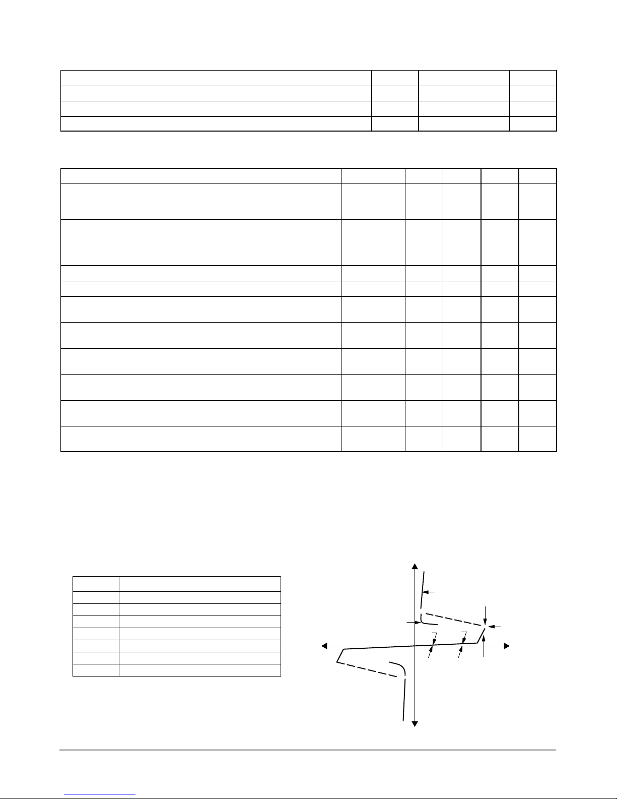
PACKAGE DIMENSIONS
SMB
CASE 403C−01
ISSUE A
*For additional information on our Pb−Free strategy and soldering
details, please download the ON Semiconductor Soldering and
Mounting Techniques Reference Manual, SOLDERRM/D.
SOLDERING FOOTPRINT*
ǒ
mm
inches
Ǔ
SCALE 8:1
2.743
0.108
2.159
0.085
2.261
0.089
A
S
D
B
J
P
K
C
H
NOTES:
1. DIMENSIONING AND TOLERANCING PER ANSI
Y14.5M, 1982.
2. CONTROLLING DIMENSION: INCH.
3. D DIMENSION SHALL BE MEASURED WITHIN
DIMENSION P.
DIM MIN MAX MIN MAX
MILLIMETERSINCHES
A 0.160 0.180 4.06 4.57
B 0.130 0.150 3.30 3.81
C 0.075 0.095 1.90 2.41
D 0.077 0.083 1.96 2.11
H 0.0020 0.0060 0.051 0.152
J 0.006 0.012 0.15 0.30
K 0.030 0.050 0.76 1.27
P 0.020 REF 0.51 REF
S 0.205 0.220 5.21 5.59
ON Semiconductor and are registered trademarks of Semiconductor Components Industries, LLC (SCILLC). SCILLC reserves the right to make changes without further notice
to any products herein. SCILLC makes no warranty, representation or guarantee regarding the suitability of its products for any particular purpose, nor does SCILLC assume any liability
arising out of the application or use of any product or circuit, and specifically disclaims any and all liability, including without limitation special, consequential or incidental damages.
“Typical” parameters which may be provided in SCILLC data sheets and/or specifications can and do vary in different applications and actual performance may vary over time. All
operating parameters, including “Typicals” must be validated for each customer application by customer’s technical experts. SCILLC does not convey any license under its patent rights
nor the rights of others. SCILLC products are not designed, intended, or authorized for use as components in systems intended for surgical implant into the body, or other applications
intended to support or sustain life, or for any other application in which the failure of the SCILLC product could create a situation where personal injury or death may occur. Should
Buyer purchase or use SCILLC products for any such unintended or unauthorized application, Buyer shall indemnify and hold SCILLC and its officers, employees, subsidiaries, affiliates,
and distributors harmless against all claims, costs, damages, and expenses, and reasonable attorney fees arising out of, directly or indirectly, any claim of personal injury or death
associated with such unintended or unauthorized use, even if such claim alleges that SCILLC was negligent regarding the design or manufacture of the part. SCILLC is an Equal
Opportunity/Affirmative Action Employer. This literature is subject to all applicable copyright laws and is not for resale in any manner.
PUBLICATION ORDERING INFORMATION
N. American Technical Support: 800−282−9855 Toll Free
USA/Canada
Europe, Middle East and Africa Technical Support:
Phone: 421 33 790 2910
Japan Customer Focus Center
Phone: 81−3−5773−3850
MMT05B350T3/D
LITERATURE FULFILLMENT:
Literature Distribution Center for ON Semiconductor
P.O. Box 5163, Denver, Colorado 80217 USA
Phone: 303−675−2175 or 800−344−3860 Toll Free USA/Canada
Fax: 303−675−2176 or 800−344−3867 Toll Free USA/Canada
Email: orderlit@onsemi.com
ON Semiconductor Website: www.onsemi.com
Order Literature: http://www.onsemi.com/orderlit
For additional information, please contact your local
Sales Representative
Page 6

Mouser Electronics
Authorized Distributor
Click to View Pricing, Inventory, Delivery & Lifecycle Information:
ON Semiconductor:
MMT05B350T3 MMT05B350T3G MMT08B350T3
 Loading...