

MMSZ4xxxET1G Series,
SZMMSZ4xxxET1G Series
Zener Voltage Regulators
500 mW SOD−123 Surface Mount
Three complete series of Zener diodes are offered in the convenient,
surface mount plastic SOD−123 package. These devices provide a
convenient alternative to the leadless 34−package style.
Features
500 mW Rating on FR−4 or FR−5 Board
Wide Zener Reverse Voltage Range − 1.8 V to 43 V
Package Designed for Optimal Automated Board Assembly
Small Package Size for High Density Applications
ESD Rating of Class 3 (> 16 kV) per Human Body Model
Peak Power − 225 W (8 x 20 ms)
AEC−Q101 Qualified and PPAP Capable
SZ Prefix for Automotive and Other Applications Requiring Unique
Site and Control Change Requirements
Pb−Free Packages are Available*
Mechanical Characteristics:
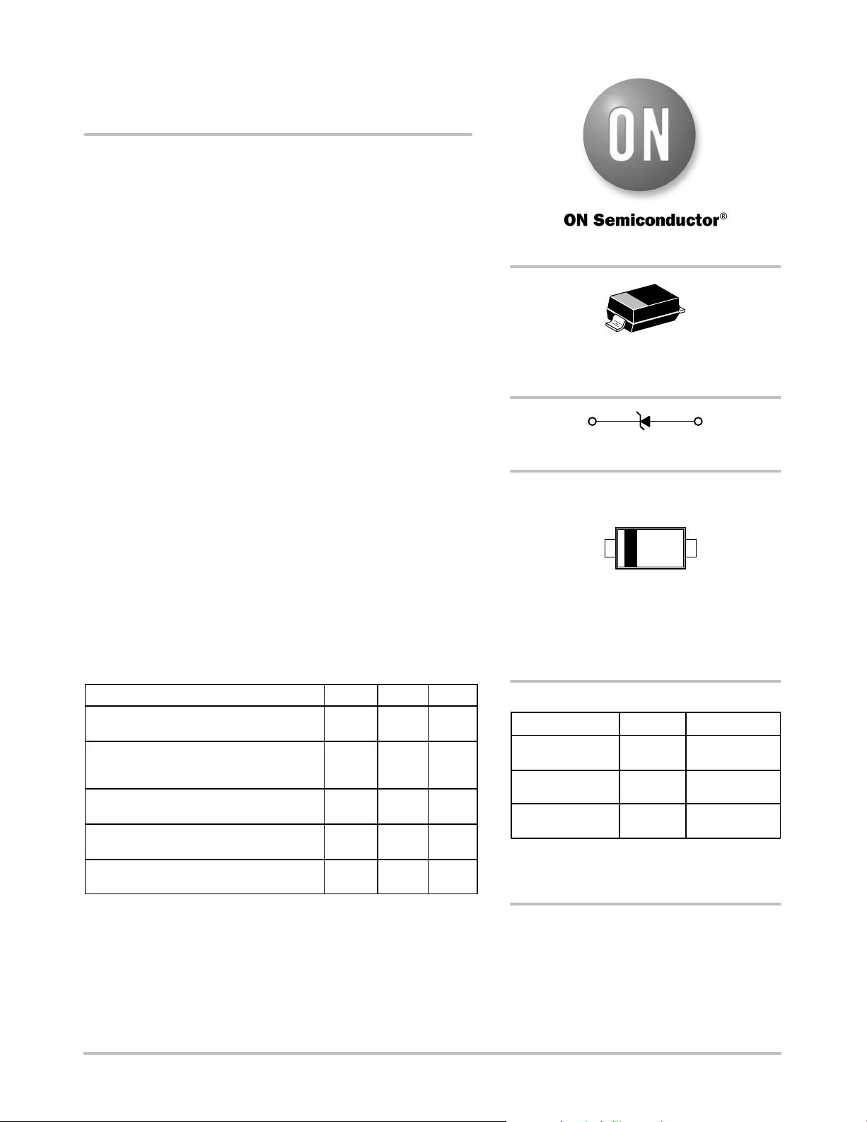
CASE:
Void-free, transfer-molded, thermosetting plastic case
FINISH: Corrosion resistant finish, easily solderable
MAXIMUM CASE TEMPERATURE FOR SOLDERING PURPOSES:
260C for 10 Seconds
POLARITY: Cathode indicated by polarity band
FLAMMABILITY RATING: UL 94 V−0
MAXIMUM RATINGS
Rating Symbol Max Unit
Peak Power Dissipation @ 20 ms (Note 1)
@ T
25C
L
Total Power Dissipation on FR−5 Board,
(Note 2) @ T
Derated above 75C
Thermal Resistance, (Note 3)
Junction−to−Ambient
Thermal Resistance, (Note 3)
Junction−to−Lead
Junction and Storage Temperature Range TJ, T
Stresses exceeding Maximum Ratings may damage the device. Maximum
Ratings are stress ratings only. Functional operation above the Recommended
Operating Conditions is not implied. Extended exposure to stresses above the
Recommended Operating Conditions may affect device reliability.
1. Nonrepetitive current pulse per Figure 11.
2. FR−5 = 3.5 x 1.5 inches, using the minimum recommended footprint.
3. Thermal Resistance measurement obtained via infrared Scan Method.
= 75C
L
P
pk
P
R
q
R
q
D
JA
JL
stg
225 W
500
6.7mWmW/C
C/W
340
C/W
150
−55 to
+150
C
http://onsemi.com
SOD−123
CASE 425
STYLE 1
1
Cathode
2
Anode
MARKING DIAGRAM
1
xxx = Device Code (Refer to page 2)
M = Date Code
G = Pb−Free Package
(Note: Microdot may be in either location)
xxx M G
G
ORDERING INFORMATION
Device Package Shipping
MMSZ4xxxET1G SOD−123
SZMMSZ4xxxET1G SOD−123
MMSZ4xxxET3G SOD−123
†For information on tape and reel specifications,
including part orientation and tape sizes, please
refer to our Tape and Reel Packaging Specifications
Brochure, BRD8011/D.
(Pb−Free)
(Pb−Free)
(Pb−Free)
Tape & Reel
Tape & Reel
10,000 /
Tape & Reel
†
3,000 /
3,000 /
DEVICE MARKING INFORMATION
See specific marking information in the device marking
column of the Electrical Characteristics table on page 2 of
this data sheet.
*For additional information on our Pb−Free strategy and soldering details, please
download the ON Semiconductor Soldering and Mounting Techniques
Reference Manual, SOLDERRM/D.
Semiconductor Components Industries, LLC, 2012
January, 2012 − Rev. 6
1 Publication Order Number:
MMSZ4678ET1/D
MMSZ4xxxET1G Series, SZMMSZ4xxxET1G Series
ELECTRICAL CHARACTERISTICS (T
otherwise noted, V
Symbol
V
Z
I
ZT
I
R
V
R
I
F
V
F
= 0.95 V Max. @ IF = 10 mA)
F
Parameter
Reverse Zener Voltage @ I
Reverse Current
Reverse Leakage Current @ V
Reverse Voltage
Forward Current
Forward Voltage @ I
F
= 25C unless
A
ZT
R
I
I
F
VRV
Z
I
V
R
F
I
ZT
V
Zener Voltage Regulator
ELECTRICAL CHARACTERISTICS (T
Device
Device*
MMSZ4680ET1G CF8 2.09 2.2 2.31 50 4 1
MMSZ4684ET1G CG3 3.13 3.3 3.47 50 7.5 1.5
MMSZ4688ET1G CG7 4.47 4.7 4.94 50 10 3
MMSZ4689ET1G CG8 4.85 5.1 5.36 50 10 3
MMSZ4690ET1G CG9 5.32 5.6 5.88 50 10 4
MMSZ4691ET1G CH1 5.89 6.2 6.51 50 10 5
MMSZ4692ET1G CH2 6.46 6.8 7.14 50 10 5.1
MMSZ4693ET1G CH3 7.13 7.5 7.88 50 10 5.7
MMSZ4697ET1G CH7 9.50 10 10.50 50 1 7.6
MMSZ4699ET1G CH9 11.40 12 12.60 50 0.05 9.1
MMSZ4701ET1G CJ2 13.3 14 14.7 50 0.05 10.6
MMSZ4702ET1G CJ3 14.25 15 15.75 50 0.05 11.4
MMSZ4703ET1G CJ4 15.20 16 16.80 50 0.05 12.1
MMSZ4705ET1G CJ6 17.10 18 18.90 50 0.05 13.6
MMSZ4709ET1G CK1 22.80 24 25.20 50 0.01 18.2
MMSZ4711ET1G CK3 25.65 27 28.35 50 0.01 20.4
MMSZ4717ET1G CK9 40.85 43 45.15 50 0.01 32.6
1. Nominal Zener voltage is measured with the device junction in thermal equilibrium at TL = 30C 1C.
*Include SZ-prefix devices where applicable.
Marking
= 25C unless otherwise noted, VF = 0.9 V Max. @ IF = 10 mA)
A
Zener Voltage (Note 1) Leakage Current
VZ (V) @ I
Min Nom Max
mA mA
ZT
IR @ V
R
V
http://onsemi.com
2

MMSZ4xxxET1G Series, SZMMSZ4xxxET1G Series
TYPICAL CHARACTERISTICS
8
7
TYPICAL TC VALUES
100
TYPICAL TC VALUES
6
5
4
3
2
VZ @ I
ZT
10
VZ @ I
ZT
1
0
−1
, TEMPERATURE COEFFICIENT (mV/ C)
VZ
−2
−3
VZ, NOMINAL ZENER VOLTAGE (V)
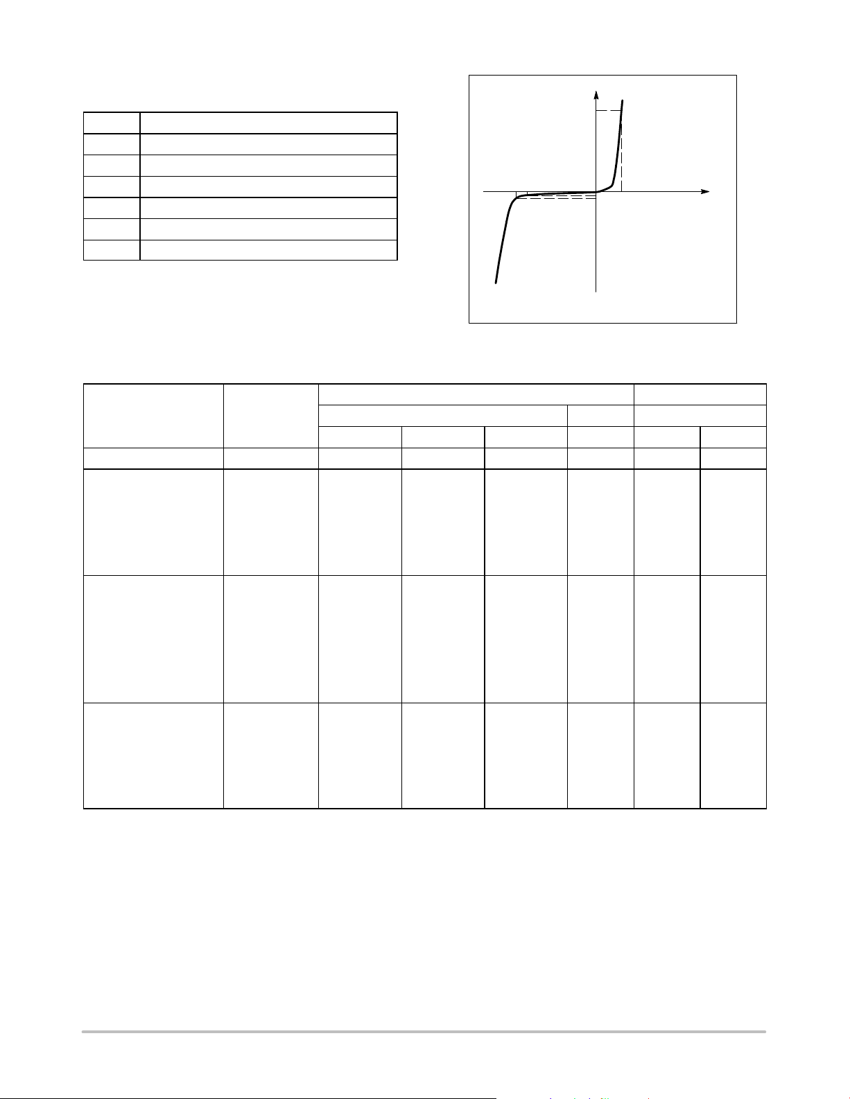
Figure 1. Temperature Coefficients
(Temperature Range −55C to +150C)
1.2
1.0
0.8
PD versus T
L
, TEMPERATURE COEFFICIENT (mV/ C)
VZ
1
12111098765432
10 100
VZ, NOMINAL ZENER VOLTAGE (V)
Figure 2. Temperature Coefficients
(Temperature Range −55C to +150C)
1000
RECTANGULAR
WAVEFORM, T
100
= 25C
A
0.6
0.4
0.2
, POWER DISSIPATION (WATTS)
D
P
1000
100
10
, DYNAMIC IMPEDANCE ( )
ZT
Z
0
IZ = 1 mA
1
PD versus T
A
T, TEMPERATURE (C)
Figure 3. Steady State Power Derating
TJ = 25C
I
= 0.1 I
Z(AC)
f = 1 kHz
5 mA
20 mA
101
, NOMINAL ZENER VOLTAGE
V
Z
Figure 5. Effect of Zener Voltage on
Zener Impedance
Z(DC)
1501251007550250
100
10
, PEAK SURGE POWER (WATTS)
pk
P
1
0.1
1 10 100 1000
PW, PULSE WIDTH (ms)
Figure 4. Maximum Nonrepetitive Surge Power
1000
75 V (MMSZ5267BT1G)
91 V (MMSZ5270BT1G)
100
10
, FORWARD CURRENT (mA)
F
I
150C
75C 25C 0C
1
VF, FORWARD VOLTAGE (V)
Figure 6. Typical Forward Voltage
1.21.11.00.90.80.70.60.50.4
http://onsemi.com
3

MMSZ4xxxET1G Series, SZMMSZ4xxxET1G Series
TYPICAL CHARACTERISTICS
1000
0 V BIAS
1 V BIAS
100
10
C, CAPACITANCE (pF)
1
100
10
1
BIAS AT
50% OF V
V
NOM
Z
101
, NOMINAL ZENER VOLTAGE (V)
Z
Figure 7. Typical Capacitance
TA = 25C
TA = 25C
100
1000
100
10
0.1
, LEAKAGE CURRENT ( A)m
0.01
R
I
0.001
0.0001
0.00001
100
10
1
+150C
+25C
−55C
80706050403020100
90
, NOMINAL ZENER VOLTAGE (V)
V
Z
Figure 8. Typical Leakage Current
TA = 25C
1
, ZENER CURRENT (mA)
Z
0.1
I
0.01
, ZENER VOLTAGE (V)
V
Z
Figure 9. Zener Voltage versus Zener Current
(V
Up to 12 V)
Z
100
90
80
70
60
50
40
30
20
% OF PEAK PULSE CURRENT
10
0
020406080
, ZENER CURRENT (mA)
Z
0.1
I
0.01
1086420
12
10 30 50 70 90
Figure 10. Zener Voltage versus Zener Current
t
P
PEAK VALUE I
PULSE WIDTH (tP) IS DEFINED
AS THAT POINT WHERE THE
PEAK CURRENT DECAY = 8 ms
HALF VALUE I
t, TIME (ms)
t
r
RSM
@ 8 ms
RSM
Figure 11. 8 20 ms Pulse Waveform
VZ, ZENER VOLTAGE (V)
(12 V to 91 V)
/2 @ 20 ms
http://onsemi.com
4

MECHANICAL CASE OUTLINE
PACKAGE DIMENSIONS
SCALE 5:1
SOD−123
CASE 425−04
ISSUE G
DATE 07 OCT 2009
D
1
H
E
2
E
b
A
A1
q
L
NOTES:
1. DIMENSIONING AND TOLERANCING PER ANSI
Y14.5M, 1982.
2. CONTROLLING DIMENSION: INCH.
MILLIMETERS INCHES
DIM MIN NOM MAX
A 0.94 1.17 1.35 0.037
A1 0.00 0.05 0.10 0.000
b 0.51 0.61 0.71 0.020
---
c
E 2.54 2.69 2.84 0.100
H
E
L 0.25
q 00
---
1.60
3.56
3.68 0.140
--- ---
--- ---
°°° °
MIN NOM MAX
0.046
0.002
0.024
--- ---
0.15
0.055D 1.40 1.80
0.063
0.010
0.106
0.145
3.86
10 10
GENERIC
MARKING DIAGRAM*
0.053
0.004
0.028
0.006
0.071
0.112
0.152
--- ---
C
SOLDERING FOOTPRINT*
0.91
0.036
1
XXX = Specific Device Code
M = Date Code
XXXMG
G
G = Pb−Free Package
2.36
0.093
4.19
0.165
SCALE 10:1
ǒ
inches
mm
1.22
0.048
Ǔ
(Note: Microdot may be in either location)
*This information is generic. Please refer to device data
sheet for actual part marking. Pb−Free indicator, “G” or
microdot “ G”, may or may not be present.
STYLE 1:
PIN 1. CATHODE
2. ANODE
*For additional information on our Pb−Free strategy and soldering
details, please download the ON Semiconductor Soldering and
Mounting Techniques Reference Manual, SOLDERRM/D.
DOCUMENT NUMBER:
DESCRIPTION:
ON Semiconductor and are trademarks of Semiconductor Components Industries, LLC dba ON Semiconductor or its subsidiaries in the United States and/or other countries.
ON Semiconductor reserves the right to make changes without further notice to any products herein. ON Semiconductor makes no warranty, representation or guarantee regarding
the suitability of its products for any particular purpose, nor does ON Semiconductor assume any liability arising out of the application or use of any product or circuit, and specifically
disclaims any and all liability, including without limitation special, consequential or incidental damages. ON Semiconductor does not convey any license under its patent rights nor the
rights of others.
© Semiconductor Components Industries, LLC, 2019
98ASB42927B
SOD−123
Electronic versions are uncontrolled except when accessed directly from the Document Repository.
Printed versions are uncontrolled except when stamped “CONTROLLED COPY” in red.
PAGE 1 OF 1
www.onsemi.com

ON Semiconductor and are trademarks of Semiconductor Components Industries, LLC dba ON Semiconductor or its subsidiaries in the United States and/or other countries.
ON Semiconductor owns the rights to a number of patents, trademarks, copyrights, trade secrets, and other intellectual property. A listing of ON Semiconductor’s product/patent
coverage may be accessed at www.onsemi.com/site/pdf/Patent−Marking.pdf
ON Semiconductor makes no warranty, representation or guarantee regarding the suitability of its products for any particular purpose, nor does ON Semiconductor assume any liability
arising out of the application or use of any product or circuit, and specifically disclaims any and all liability, including without limitation special, consequential or incidental damages.
Buyer is responsible for its products and applications using ON Semiconductor products, including compliance with all laws, regulations and safety requirements or standards,
regardless of any support or applications information provided by ON Semiconductor. “Typical” parameters which may be provided in ON Semiconductor data sheets and/or
specifications can and do vary in different applications and actual performance may vary over time. All operating parameters, including “Typicals” must be validated for each customer
application by customer’s technical experts. ON Semiconductor does not convey any license under its patent rights nor the rights of others. ON Semiconductor products are not
designed, intended, or authorized for use as a critical component in life support systems or any FDA Class 3 medical devices or medical devices with a same or similar classification
in a foreign jurisdiction or any devices intended for implantation in the human body. Should Buyer purchase or use ON Semiconductor products for any such unintended or unauthorized
application, Buyer shall indemnify and hold ON Semiconductor and its officers, employees, subsidiaries, affiliates, and distributors harmless against all claims, costs, damages, and
expenses, and reasonable attorney fees arising out of, directly or indirectly, any claim of personal injury or death associated with such unintended or unauthorized use, even if such
claim alleges that ON Semiconductor was negligent regarding the design or manufacture of the part. ON Semiconductor is an Equal Opportunity/Affirmative Action Employer. This
literature is subject to all applicable copyright laws and is not for resale in any manner.
. ON Semiconductor reserves the right to make changes without further notice to any products herein.
PUBLICATION ORDERING INFORMATION
LITERATURE FULFILLMENT:
Email Requests to: orderlit@onsemi.com
ON Semiconductor Website: www.onsemi.com
TECHNICAL SUPPORT
North American Technical Support:
Voice Mail: 1 800−282−9855 Toll Free USA/Canada
Phone: 011 421 33 790 2910
Europe, Middle East and Africa Technical Support:
Phone: 00421 33 790 2910
For additional information, please contact your local Sales Representative
◊
www.onsemi.com
1
 Loading...