

Page 1
MMFT960T1
l
l
s
Preferred Device
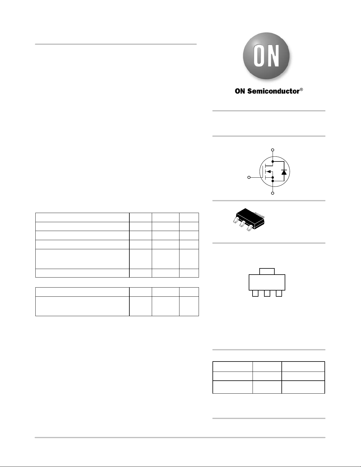
Power MOSFET
300 mA, 60 Volts
N−Channel SOT−223
This Power MOSFET is designed for high speed, low loss power
switching applications such as switching regulators, dc−dc converters,
solenoid and relay drivers. The device is housed in the SOT−223
package which is designed for medium power surface mount
applications.
Features
• Silicon Gate for Fast Switching Speeds
• Low Drive Requirement
• The SOT−223 Package can be Soldered Using Wave or Reflow
• The Formed Leads Absorb Thermal Stress During Soldering
Eliminating the Possibility of Damage to the Die
• Pb−Free Package is Available
MAXIMUM RATINGS (T
Rating Symbol Value Unit
Drain−to−Source Voltage V
Gate−to−Source Voltage − Non−Repetitive V
Drain Current I
Total Power Dissipation @ TA = 25°C
(Note 1)
Derate above 25°C
Operating and Storage Temperature Range TJ, T
THERMAL CHARACTERISTICS
Thermal Resistance, Junction−to−Ambient
Maximum Temperature for Soldering
Purposes
Time in Solder Bath
Maximum ratings are those values beyond which device damage can occur.
Maximum ratings applied to the device are individual stress limit values (not
normal operating conditions) and are not valid simultaneously. If these limits are
exceeded, device functional operation is not implied, damage may occur and
reliability may be affected.
1. Device mounted on a FR−4 glass epoxy printed circuit board using minimum
recommended footprint.
= 25°C unless otherwise noted)
C
DS
GS
D
P
D
stg
R
q
JA
T
L
60 V
± 30 V
300 mAdc
0.8
6.4
−65 to 150 °C
156 °C/W
260
10
W
mW/°C
°C
S
http://onsemi.com
300 mA, 60 VOLTS
R
DS(on)
G
1
2
3
MARKING DIAGRAM AND
PIN ASSIGNMENT
Gate
A = Assembly Location
Y = Year
W = Work Week
G = Pb−Free Package
FT960 = Device Code
(Note: Microdot may be in either location)
ORDERING INFORMATION
Device Package Shipping
MMFT960T1 SOT−223 1000 Tape & Ree
MMFT960T1G SOT−223
†For information on tape and reel specifications,
including part orientation and tape sizes, please
refer to our Tape and Reel Packaging Specification
Brochure, BRD8011/D.
Preferred devices are recommended choices for future use
and best overall value.
N−Channel
4
4 Drain
AYW
FT960 G
G
2
1
Drain
(Pb−Free)
= 1.7 W
D
S
TO−261AA
CASE 318E
STYLE 3
3
Source
†
1000 Tape & Ree
© Semiconductor Components Industries, LLC, 2006
January, 2006 − Rev. 5
1
Publication Order Number:
MMFT960T1/D
Page 2
MMFT960T1
ELECTRICAL CHARACTERISTICS (T
= 25°C unless otherwise noted)
A
Characteristic Symbol Min Typ Max Unit
OFF CHARACTERISTICS
Drain−to−Source Breakdown Voltage
(VGS = 0, ID = 10 mA)
Zero Gate Voltage Drain Current
(V
= 60 V, VGS = 0)
DS
Gate−Body Leakage Current
(VGS = 15 Vdc, VDS = 0)
ON CHARACTERISTICS (Note 2)
Gate Threshold Voltage
(VDS = VGS, ID = 1.0 mAdc)
Static Drain−to−Source On−Resistance
(VGS = 10 Vdc, ID = 1.0 A)
Drain−to−Source On−Voltage
(VGS = 10 V, ID = 0.5 A)
(VGS = 10 V, ID = 1.0 A)
Forward Transconductance
(VDS = 25 V, ID = 0.5 A)
DYNAMIC CHARACTERISTICS
Input Capacitance
Output Capacitance C
(VDS = 25 V, V
= 0, f = 1.0 MHz)
GS
Transfer Capacitance C
Total Gate Charge
Gate−Source Charge Q
(VGS = 10 V, ID = 1.0 A, VDS = 48 V)
Gate−Drain Charge Q
2. Pulse Test: Pulse Width ≤ 300 ms, Duty Cycle ≤ 2.0%.
V
(BR)DSS
I
DSS
I
GSS
V
GS(th)
R
DS(on)
V
DS(on)
g
C
oss
Q
iss
rss
gd
60 − − Vdc
− − 10
mAdc
− − 50 nAdc
1.0 − 3.5 Vdc
− − 1.7
W
Vdc
−
−
fs
− 600 − mmhos
− 65 −
−
−
0.8
1.7
pF
− 33 −
− 7.0 −
g
gs
− 3.2 −
− 1.2 −
nC
− 2.0 −
5
4
3
2
, DRAIN CURRENT (AMPS)
D
I
1
0
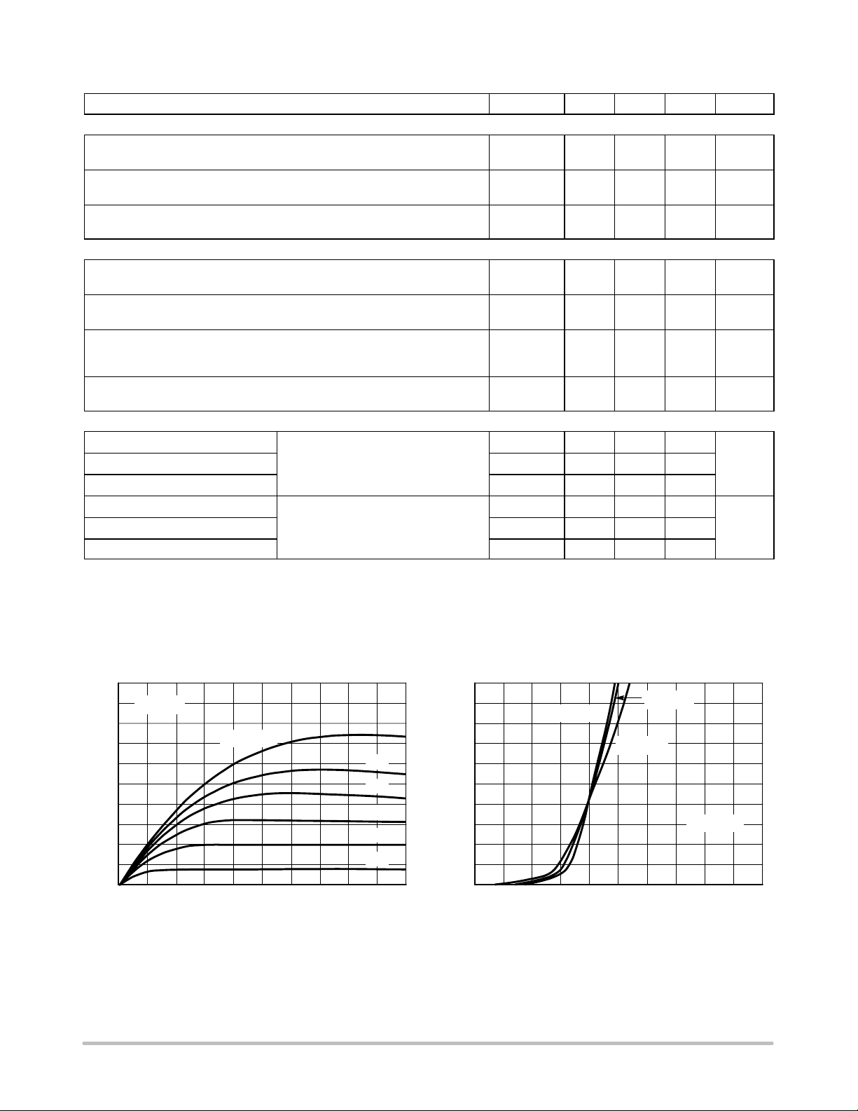
TYPICAL ELECTRICAL CHARACTERISTICS
1
TJ = 25°C
0.8
TJ = −55°C
VGS = 10 V
8 V
0.6
7 V
6 V
5 V
0.4
, DRAIN CURRENT (AMPS)
D
I
0.2
4 V
1086420
VDS, DRAIN−TO−SOURCE VOLTAGE (VOLTS)
0
VGS, GATE−TO−SOURCE VOLTAGE (VOLTS)
Figure 1. On−Region Characteristics Figure 2. Transfer Characteristics
http://onsemi.com
2
TJ = 25°C
TJ = 125°C
VDS = 10 V
1086420
Page 3

MMFT960T1
e
TYPICAL ELECTRICAL CHARACTERISTICS
5
VGS = 10 V
4
3
TJ = 125°C
2
1
, DRAIN−SOURCE RESISTANCE (OHMS)
DS(on)
R
0
0.50
1 1.5 2 2.5
ID, DRAIN CURRENT (AMPS)
Figure 3. On−Resistance versus Drain Current
1
TJ = 125°C
0.1
, DRAIN CURRENT (AMPS)
D
I
0
0.3 0.6 0.9 1.2 1.5
VSD, SOURCE−DRAIN DIODE FORWARD VOLTAGE (VOLTS)
TJ = 25°C
Figure 5. Source−Drain Diode Forward Voltage
25°C
−55 °C
10
ID = 1 A
V
= 10 V
GS
1
, DRAIN−SOURCE RESISTANCE (NORMALIZED)
0.1
−75 −50 −25 0 25 50 75 100 125 150
DS(on)
R
TJ, JUNCTION TEMPERATURE (°C)
Figure 4. On−Resistance Variation with Temperatur
250
225
200
175
150
125
100
75
C, CAPACITANCE (pF)
50
25
0
0 5 10 15 20 25 30
, DRAIN−SOURCE VOLTAGE (VOLTS)
V
DS
C
C
iss
C
oss
rss
VGS = 0 V
f = 1 MHz
TJ = 25°C
Figure 6. Capacitance Variation
10
9
ID = 1 A
TJ = 25°C
0 0.5 1 1.5 2 2.5 3 3.5 4
VDS = 30 V
VDS = 48 V
Qg, TOTAL GATE CHARGE (nC)
, GATE−TO−SOURCE VOLTAGE (VOLTS)
GS
V
8
7
6
5
4
3
2
1
0
Figure 7. Gate Charge versus Gate−to−Source Voltage
http://onsemi.com
2
VDS = 10 V
1.5
1
TJ = −55°C
0.5
, TRANSCONDUCTANCE (mhos)
FS
g
125°C
0
0.50 1 1.5 2 2.5
ID, DRAIN CURRENT (AMPS)
25°C
Figure 8. Transconductance
3
Page 4

MMFT960T1
PACKAGE DIMENSIONS
SOT−223 (TO−261)
CASE 318E−04
ISSUE L
0.08 (0003)
H
e1
E
A1
D
b1
4
123
e
E
b
q
A
SOLDERING FOOTPRINT*
3.8
0.15
2.0
0.079
L1
NOTES:
1. DIMENSIONING AND TOLERANCING PER ANSI
Y14.5M, 1982.
2. CONTROLLING DIMENSION: INCH.
DIMAMIN NOM MAX MIN
A1 0.02 0.06 0.10 0.001
b 0.60 0.75 0.89 0.024
b1 2.90 3.06 3.20 0.115
c 0.24 0.29 0.35 0.009
D 6.30 6.50 6.70 0.249
E 3.30 3.50 3.70 0.130
e 2.20 2.30 2.40 0.087
e1
L1 1.50 1.75 2.00 0.060
H
C
E
q
STYLE 3:
PIN 1. GATE
MILLIMETERS
1.50 1.63 1.75 0.060
0.85 0.94 1.05 0.033
6.70 7.00 7.30 0.264
0° 10° 0° 10°
2. DRAIN
3. SOURCE
4. DRAIN
INCHES
NOM MAX
0.064 0.068
0.002 0.004
0.030 0.035
0.121 0.126
0.012 0.014
0.256 0.263
0.138 0.145
0.091 0.094
0.037 0.041
0.069 0.078
− −
0.276 0.287
2.3
0.091
2.3
0.091
6.3
0.248
2.0
0.079
1.5
0.059
SCALE 6:1
ǒ
inches
mm
Ǔ
*For additional information on our Pb−Free strategy and soldering
details, please download the ON Semiconductor Soldering and
Mounting Techniques Reference Manual, SOLDERRM/D.
ON Semiconductor and are registered trademarks of Semiconductor Components Industries, LLC (SCILLC). SCILLC reserves the right to make changes without further notice
to any products herein. SCILLC makes no warranty, representation or guarantee regarding the suitability of its products for any particular purpose, nor does SCILLC assume any liability
arising out of the application or use of any product or circuit, and specifically disclaims any and all liability, including without limitation special, consequential or incidental damages.
“Typical” parameters which may be provided in SCILLC data sheets and/or specifications can and do vary in different applications and actual performance may vary over time. All
operating parameters, including “Typicals” must be validated for each customer application by customer’s technical experts. SCILLC does not convey any license under its patent rights
nor the rights of others. SCILLC products are not designed, intended, or authorized for use as components in systems intended for surgical implant into the body, or other applications
intended to support or sustain life, or for any other application in which the failure of the SCILLC product could create a situation where personal injury or death may occur. Should
Buyer purchase or use SCILLC products for any such unintended or unauthorized application, Buyer shall indemnify and hold SCILLC and its officers, employees, subsidiaries, affiliates,
and distributors harmless against all claims, costs, damages, and expenses, and reasonable attorney fees arising out of, directly or indirectly, any claim of personal injury or death
associated with such unintended or unauthorized use, even if such claim alleges that SCILLC was negligent regarding the design or manufacture of the part. SCILLC is an Equal
Opportunity/Affirmative Action Employer. This literature is subject to all applicable copyright laws and is not for resale in any manner.
PUBLICATION ORDERING INFORMATION
LITERATURE FULFILLMENT:
Literature Distribution Center for ON Semiconductor
P.O. Box 61312, Phoenix, Arizona 85082−1312 USA
Phone: 480−829−7710 or 800−344−3860 Toll Free USA/Canada
Fax: 480−829−7709 or 800−344−3867 Toll Free USA/Canada
Email: orderlit@onsemi.com
N. American Technical Support: 800−282−9855 Toll Free
USA/Canada
Japan: ON Semiconductor, Japan Customer Focus Center
2−9−1 Kamimeguro, Meguro−ku, Tokyo, Japan 153−0051
Phone: 81−3−5773−3850
http://onsemi.com
ON Semiconductor Website: http://onsemi.com
Order Literature: http://www.onsemi.com/litorder
For additional information, please contact your
local Sales Representative.
MMFT960T1/D
4
 Loading...