

查询MCR08B供应商
MCR08B, MCR08M
Preferred Device
Sensitive Gate
Silicon Controlled Rectifiers
Reverse Blocking Thyristors
PNPN devices designed for line powered consumer applications
such as relay and lamp drivers, small motor controls, gate drivers for
larger thyristors, and sensing and detection circuits. Supplied in
surface mount package for use in automated manufacturing.
• Sensitive Gate Trigger Current
• Blocking Voltage to 600 Volts
• Glass Passivated Surface for Reliability and Uniformity
• Surface Mount Package
• Device Marking: MCR08BT1: CR08B; MCR08MT1: CR08M, and
Date Code
http://onsemi.com
SCRs
0.8 AMPERES RMS
200 thru 600 VOLTS
G
A
K
MAXIMUM RATINGS (T
Rating Symbol Value Unit
Peak Repetitive Off–State V oltage
(Sine Wave, RGK = 1000 Ω,
TJ = 25 to 110°C)
On-State Current RMS
(All Conduction Angles; TC = 80°C)
Peak Non-repetitive Surge Current
(1/2 Cycle Sine Wave, 60 Hz,
TC = 25°C)
Circuit Fusing Considerations
(t = 8.3 ms)
Forward Peak Gate Power
(TC = 80°C, t = 1.0 µs)
Average Gate Power
(TC = 80°C, t = 8.3 ms)
Operating Junction Temperature Range T
Storage Temperature Range T
(1) V
and V
DRM
apply for zero or negative gate voltage; however, positive gate voltage shall
not be applied concurrent with negative potential on the anode. Blocking
voltages shall not be tested with a constant source such that the voltage
ratings of the devices are exceeded.
RRM
= 25°C unless otherwise noted)
J
(1)
MCR08BT1
MCR08MT1
for all types can be applied on a continuous basis. Ratings
V
DRM,
V
RRM
200
600
I
T(RMS)
I
TSM
I2t 0.4 A2s
P
GM
P
G(AV)
J
stg
0.8 Amps
8.0 Amps
0.1 Watts
0.01 Watts
–40 to
+110
–40 to
+150
Volts
°C
°C
4
1
2
3
SOT–223
CASE 318E
STYLE 10
PIN ASSIGNMENT
1
2
3
4
Cathode
Anode
Gate
Anode
ORDERING INFORMATION
Device Package Shipping
MCR08BT1 SOT223 16mm Tape and Reel
MCR08MT1 SOT223
Preferred devices are recommended choices for future use
and best overall value.
(1K/Reel)
16mm Tape and Reel
(1K/Reel)
Semiconductor Components Industries, LLC, 2000
May, 2000 – Rev. 3
1 Publication Order Number:
MCR08BT1/D
MCR08B, MCR08M
THERMAL CHARACTERISTICS
Characteristic Symbol Value Unit
Thermal Resistance, Junction to Ambient
PCB Mounted per Figure 1
Thermal Resistance, Junction to Tab
Measured on Anode Tab Adjacent to Epoxy
Maximum Device Temperature for Soldering Purposes (for 10 Seconds Maximum) T
ELECTRICAL CHARACTERISTICS (T
Characteristic
OFF CHARACTERISTICS
Peak Repetitive Forward or Reverse Blocking Current
(VAK = Rated V
DRM
or V
, RGK = 1000 Ω)T
RRM
ON CHARACTERISTICS
Peak Forward On-State Voltage
(IT = 1.0 A Peak)
Gate Trigger Current (Continuous dc)
(VAK = 12 Vdc, RL = 100 Ω)
Holding Current
(VAK = 12 Vdc, Initiating Current = 20 mA)
Gate Trigger Voltage (Continuous dc)
(VAK = 12 Vdc, RL = 100 Ω)
(3)
(1)
DYNAMIC CHARACTERISTICS
Critical Rate-of-Rise of Off State V oltage
(Vpk = Rated V
(1) Pulse Test: Pulse Width ≤ 300 µs, Duty Cycle ≤ 2%.
(2) RGK = 1000 Ω is included in measurement.
(3) RGK is not included in measurement.
, TC = 110°C, RGK = 1000 Ω, Exponential Method)
DRM
= 25°C unless otherwise noted)
C
(2)
(3)
(3)
= 25°C
J
TJ = 110°C
Symbol Min Typ Max Unit
I
DRM
R
θJA
R
θJT
L
, I
RRM
V
TM
I
GT
I
H
V
GT
dv/dt 10 — — V/µs
—
—
— — 1.7 Volts
— — 200 µA
— — 5.0 mA
— — 0.8 Volts
156 °C/W
25 °C/W
260 °C
—
—
10
200
µA
µA
http://onsemi.com
2
MCR08B, MCR08M
Voltage Current Characteristic of SCR
+ Current
Anode +
Symbol Parameter
V
DRM
I
DRM
V
RRM
I
RRM
V
TM
I
H
Peak Repetitive Off State Forward Voltage
Peak Forward Blocking Current
Peak Repetitive Off State Reverse Voltage
Peak Reverse Blocking Current
Peak On State Voltage
Holding Current
0.079
2.0
0.079
2.0
0.984
25.0
0.059
1.5
0.091
2.3
0.15
3.8
0.059
1.5
0.091
2.3
0.059
1.5
0.244
6.2
inches
ǒ
mm
V
TM
on state
I
I
at V
RRM
Reverse Avalanche Region
Anode –
Ǔ
BOARD MOUNTED VERTICALL Y IN CINCH 8840 EDGE CONNECT OR.
RRM
Reverse Blocking Region
(off state)
BOARD THICKNESS = 65 MIL., FOIL THICKNESS = 2.5 MIL.
MATERIAL: G10 FIBERGLASS BASE EPOXY
H
Forward Blocking Region
(off state)
I
DRM
at V
+ Voltage
DRM
0.096
2.44
0.096
2.44
0.059
1.5
0.472
12.0
0.096
2.44
0.059
1.5
Figure 1. PCB for Thermal Impedance and
Power Testing of SOT-223
http://onsemi.com
3
MCR08B, MCR08M
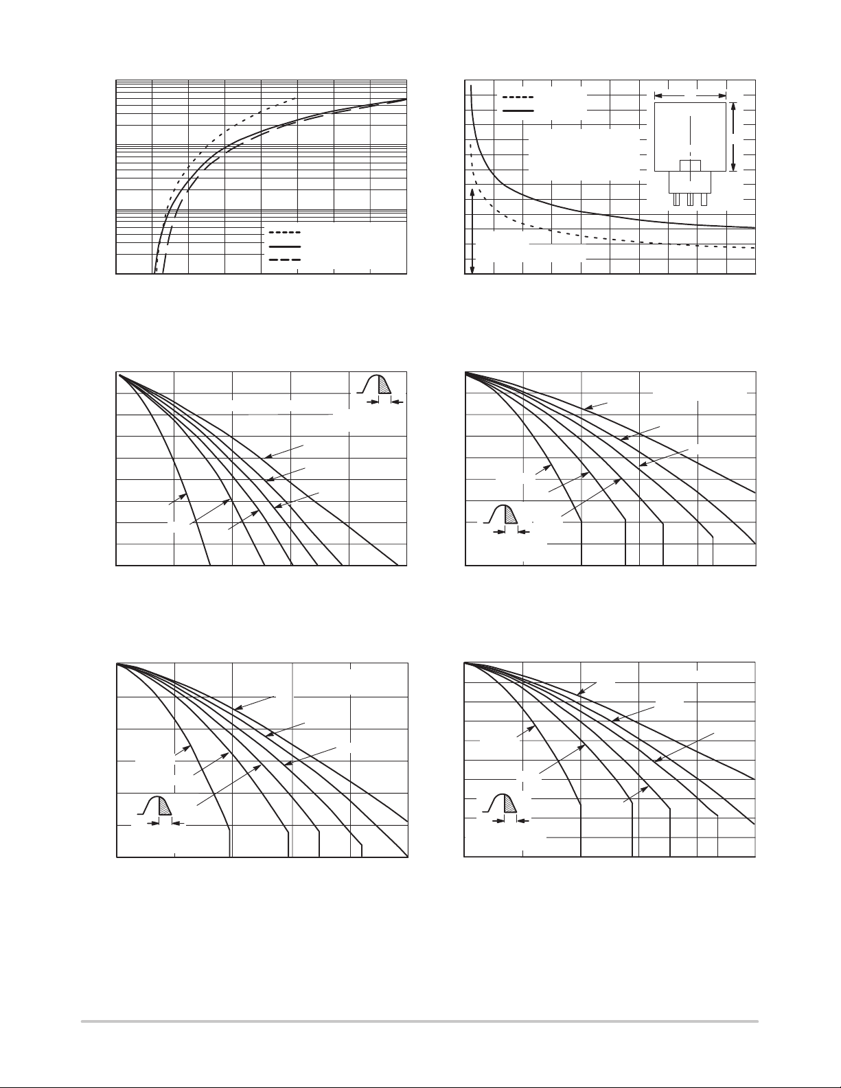
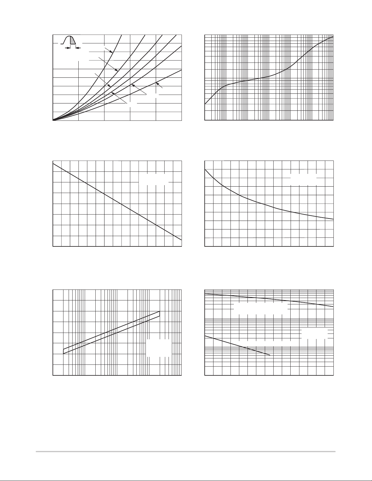
, INSTANTANEOUS ON-STATE CURRENT (AMPS)
I
, MAXIMUM ALLOWABLE
A
T
T
AMBIENT TEMPERATURE ( C)°
1.0
0.1
0.01
110
100
10
TYPICAL AT TJ = 110°C
MAX AT TJ = 110°C
MAX AT TJ = 25°C
0
2.0 3.0
4.01.0
160
150
140
130
°THERMAL RESISTANCE, ( C/W)
120
110
100
90
80
70
60
θJA
R , JUNCTION TO AMBIENT
50
40
30
TYPICAL
MAXIMUM
DEVICE MOUNTED ON
FIGURE 1 AREA = L
PCB WITH TAB AREA
AS SHOWN
MINIMUM
FOOTPRINT = 0.076 cm
2.00 4.0 6.0 8.0 10
1.0 3.0 5.0 7.0 9.0
FOIL AREA (cm2)vT, INSTANTANEOUS ON-STATE VOLTAGE (VOLTS)
2
2
L
4
1 23
L
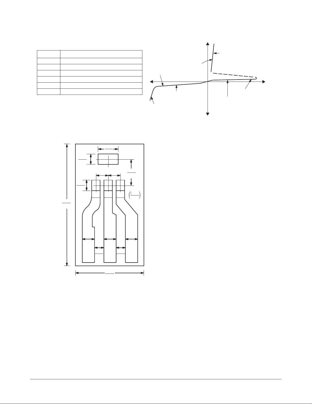
Figure 2. On-State Characteristics Figure 3. Junction to Ambient Thermal
Resistance versus Copper T ab Area
110
, MAXIMUM ALLOWABLE
A
T
100
90
80
70
60
50
40
AMBIENT TEMPERATURE ( C)°
30
20
α = 30°
α
α = CONDUCTION
ANGLE
I
T(AV)
60°
90°
, AVERAGE ON-ST ATE CURRENT (AMPS)
0.4
α
ANGLE
0.5
90
80
70
60
50
α = 30°
40
30
20
60°
I
T(AV)
50 OR 60 Hz HALFWA VE
90°
0.30.20.10
, AVERAGE ON-STATE CURRENT (AMPS)
α = CONDUCTION
dc
180°
120°
dc
1.0 cm2 FOIL, 50 OR
60 Hz HALFWA VE
180°
120°
0.40.30.20.10
0.5
, MAXIMUM ALLOWABLE
A
T
Figure 4. Current Derating, Minimum Pad Size
Reference: Ambient T emperature
110
100
90
80
70
AMBIENT TEMPERATURE ( C)°
60
50
α = 30°
60°
α
α = CONDUCTION
ANGLE
I
T(AV)
90°
, AVERAGE ON-STATE CURRENT (AMPS)
PAD AREA = 4.0 cm2, 50
OR 60 Hz HALFWA VE
dc
180°
Figure 6. Current Derating, 2.0 cm Square Pad
Reference: Ambient T emperature
120°
0.40.30.20.10
0.5
, MAXIMUM ALLOWABLE
(tab)
T
Figure 5. Current Derating, 1.0 cm Square Pad
Reference: Ambient T emperature
110
TAB TEMPERATURE ( C)°
85
α = 30°
60°
α
α = CONDUCTION
ANGLE
I
T(AV)
dc
90°
, AVERAGE ON-STATE CURRENT (AMPS)
50 OR 60 Hz HALFWA VE
Figure 7. Current Derating
Reference: Anode T ab
180°
120°
0.50.40.30.20.10
http://onsemi.com
4
MCR08B, MCR08M
1.0
0.9
0.8
0.7
0.6
0.5
0.4
,DISSIPATION (WATTS)
0.3
(AV)
0.2
MAXIMUM AVERAGE POWER
P
0.1
α = CONDUCTION
0
0.7
0.6
0.5
ANGLE
α
α = 30°
60°
90°
0.30.20.10
I
, AVERAGE ON-STATE CURRENT (AMPS)
T(AV)
Figure 8. Power Dissipation
120°
180°
0.4
VAK = 12 V
RL = 100 Ω
1.0
0.1
0.5
NORMALIZED
, TRANSIENT THERMAL RESISTANCE
T
r
0.01
0.001 0.01 1.0 10
t, TIME (SECONDS)
1000.10.0001
dc
Figure 9. Thermal Response Device
Mounted on Figure 1 Printed Circuit Board
2.0
VAK = 12 V
RL = 3.0 kΩ
1.0
, GATE TRIGGER VOLTAGE (VOLTS)
GT
V
, GATE TRIGGER VOLTAGE (VOLTS)
GT
V
0.4
0.3
0.7
0.65
0.6
0.55
0.5
0.45
0.4
0.35
0.3
8020–40 –20 0 40 60 110
TJ, JUNCTION TEMPERATURE, (°C)
Figure 10. T ypical Gate Trigger Voltage
versus Junction T emperature
VAK = 12 V
RL = 100 Ω
TJ = 25°C
1.0 100
IGT, GATE TRIGGER CURRENT (µA)
(NORMALIZED)
, HOLDING CURRENT
H
I
0
1000
A)
100
10
, GATE TRIGGER CURRENT (µ
GT
I
1000100.1
1.0
8020–40 –20 0 40 60 110
TJ, JUNCTION TEMPERATURE, (°C)
Figure 11. Typical Normalized Holding Current
versus Junction T emperature
RGK = 1000 Ω, RESISTOR
CURRENT INCLUDED
VAK = 12 V
RL = 100 Ω
WITHOUT GATE RESISTOR
8020–40 –20 0 40 60 110
TJ, JUNCTION TEMPERATURE (°C)
Figure 12. T ypical Range of VGT
versus Measured I
GT
Figure 13. T ypical Gate Trigger Current
versus Junction T emperature
http://onsemi.com
5
MCR08B, MCR08M
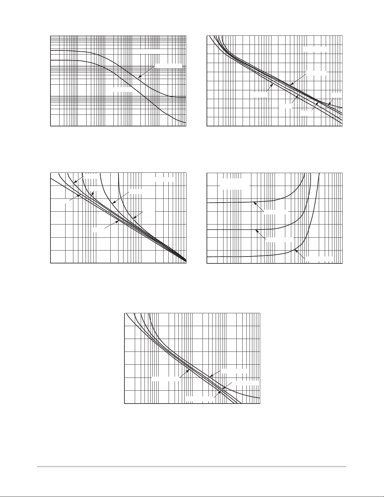
100
1.0
HOLDING CURRENT (mA)I ,
H
0.1
10000
1000
500
100
10
IGT = 7 µA
10 100 10,000 100,000
RGK, GATE-CATHODE RESISTANCE (OHMS)
10001.0
Figure 14. Holding Current Range versus
Gate-Cathode Resistance
300 V
200 V
400 V
100 V
TJ = 25°C
TJ = 110°C
50 V
IGT = 48 µA
10000
5000
1000
500
100
50
10
5.0
STATIC dv/dt (V/ S)µ
1.0
0.5
0.1
10 100 1000 10,000 100,000
RGK, GATE-CATHODE RESISTANCE (OHMS)
125°
110°
Vpk = 400 V
TJ = 25°
75°
Figure 15. Exponential Static dv/dt versus Junction
T emperature and Gate-Cathode Termination Resistance
10000
1000
500
100
TJ = 110°C
400 V (PEAK)
RGK = 100
50°
50
10
STATIC dv/dt (V/ S)µ
5.0
1.0
500 V
RGK, GATE-CATHODE RESISTANCE (OHMS)
Figure 16. Exponential Static dv/dt versus Peak
V oltage and Gate-Cathode Termination Resistance
10000
1000
500
100
50
10
STATIC dv/dt (V/ S)µ
5.0
1.0
IGT = 5 µA
100 1000 10,000 100,00010
50
10
STATIC dv/dt (V/ S)µ
5.0
10,00010 100 1000
1.0
0.01
Figure 17. Exponential Static dv/dt versus
Gate-Cathode Capacitance and Resistance
IGT = 70 µA
IGT = 15 µA
GATE-CATHODE RESISTANCE (OHMS)
RGK = 1.0 k
RGK = 10 k
0.1 1.0 10 100
CGK, GATE-CATHODE CAPACITANCE (nF)
IGT = 35 µA
Figure 18. Exponential Static dv/dt versus
Gate-Cathode Termination Resistance and
Product Trigger Current Sensitivity
http://onsemi.com
6
MCR08B, MCR08M
INFORMATION FOR USING THE SOT-223 SURFACE MOUNT PACKAGE
MINIMUM RECOMMENDED FOOTPRINT FOR SURFACE MOUNTED APPLICATIONS
Surface mount board layout is a critical portion of the
total design. The footprint for the semiconductor packages
must be the correct size to insure proper solder connection
0.079
2.0
0.091
2.3
0.079
2.0
0.059
1.5
SOT-223
SOT-223 POWER DISSIPATION
The power dissipation of the SOT -223 is a function of the
anode pad size. This can vary from the minimum pad size
for soldering to a pad size given for maximum power
dissipation. Power dissipation for a surface mount device is
determined by T
temperature of the die, R
, the maximum rated junction
J(max)
, the thermal resistance from
θJA
the device junction to ambient, and the operating
temperature, TA. Using the values provided on the data
sheet for the SOT-223 package, PD can be calculated as
follows:
PD =
T
J(max)
R
θJA
– T
A
The values for the equation are found in the maximum
ratings table on the data sheet. Substituting these values
into the equation for an ambient temperature TA of 25°C,
one can calculate the power dissipation of the device which
in this case is 550 milliwatts.
110°C – 25°C
PD =
156°C/W
= 550 milliwatts
interface between the board and the package. With the
correct pad geometry, the packages will self align when
subjected to a solder reflow process.
0.15
3.8
0.248
6.3
inches
mm
0.059
1.5
0.091
2.3
0.059
1.5
The 156°C/W for the SOT-223 package assumes the use
of the recommended footprint on a glass epoxy printed
circuit board to achieve a power dissipation of 550
milliwatts. There are other alternatives to achieving higher
power dissipation from the SOT-223 package. One is to
increase the area of the anode pad. By increasing the area of
the anode pad, the power dissipation can be increased.
Although one can almost double the power dissipation with
this method, one will be giving up area on the printed
circuit board which can defeat the purpose of using surface
mount technology . A graph of R
versus anode pad area
θJA
is shown in Figure 3.
Another alternative would be to use a ceramic substrate
or an aluminum core board such as Thermal Clad. Using
a board material such as Thermal Clad, an aluminum core
board, the power dissipation can be doubled using the same
footprint.
SOLDER STENCIL GUIDELINES
Prior to placing surface mount components onto a printed
circuit board, solder paste must be applied to the pads. A
solder stencil is required to screen the optimum amount of
solder paste onto the footprint. The stencil is made of brass
http://onsemi.com
or stainless steel with a typical thickness of 0.008 inches.
The stencil opening size for the SOT-223 package should
be the same as the pad size on the printed circuit board, i.e.,
a 1:1 registration.
7
MCR08B, MCR08M
SOLDERING PRECAUTIONS
The melting temperature of solder is higher than the rated
temperature of the device. When the entire device is heated
to a high temperature, failure to complete soldering within
a short time could result in device failure. Therefore, the
following items should always be observed in order to
minimize the thermal stress to which the devices are
subjected.
• Always preheat the device.
• The delta temperature between the preheat and
soldering should be 100°C or less.*
• When preheating and soldering, the temperature of the
leads and the case must not exceed the maximum
temperature ratings as shown on the data sheet. When
using infrared heating with the reflow soldering
method, the difference should be a maximum of 10°C.
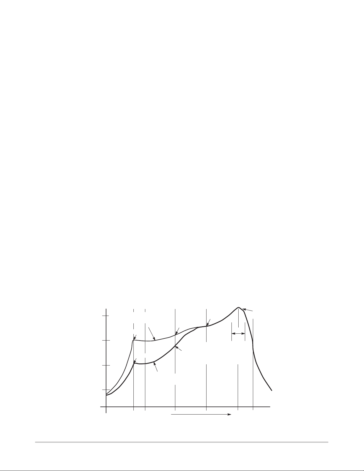
TYPICAL SOLDER HEATING PROFILE
For any given circuit board, there will be a group of
control settings that will give the desired heat pattern. The
operator must set temperatures for several heating zones,
and a figure for belt speed. Taken together, these control
settings make up a heating “profile” for that particular
circuit board. On machines controlled by a computer, the
computer remembers these profiles from one operating
session to the next. Figure 19 shows a typical heating
profile for use when soldering a surface mount device to a
printed circuit board. This profile will vary among
soldering systems but it is a good starting point. Factors that
can affect the profile include the type of soldering system in
use, density and types of components on the board, type of
solder used, and the type of board or substrate material
being used. This profile shows temperature versus time.
• The soldering temperature and time should not exceed
260°C for more than 10 seconds.
• When shifting from preheating to soldering, the
maximum temperature gradient should be 5°C or less.
• After soldering has been completed, the device should
be allowed to cool naturally for at least three minutes.
Gradual cooling should be used as the use of forced
cooling will increase the temperature gradient and
result in latent failure due to mechanical stress.
• Mechanical stress or shock should not be applied
during cooling.
* Soldering a device without preheating can cause
excessive thermal shock and stress which can result in
damage to the device.
The line on the graph shows the actual temperature that
might be experienced on the surface of a test board at or
near a central solder joint. The two profiles are based on a
high density and a low density board. The Vitronics
SMD310 convection/infrared reflow soldering system was
used to generate this profile. The type of solder used was
62/36/2 Tin Lead Silver with a melting point between
177–189°C. When this type of furnace is used for solder
reflow work, the circuit boards and solder joints tend to
heat first. The components on the board are then heated by
conduction. The circuit board, because it has a large surface
area, absorbs the thermal energy more efficiently, then
distributes this energy to the components. Because of this
effect, the main body of a component may be up to 30
degrees cooler than the adjacent solder joints.
200°C
150°C
100°C
50°C
STEP 1
PREHEAT
ZONE 1
“RAMP”
DESIRED CURVE FOR HIGH
TIME (3 TO 7 MINUTES TOTAL)
STEP 2
VENT
“SOAK”
MASS ASSEMBLIES
150°C
100°C
Figure 19. T ypical Solder Heating Profile
STEP 3
HEATING
ZONES 2 & 5
“RAMP”
DESIRED CURVE FOR LOW
STEP 4
HEATING
ZONES 3 & 6
“SOAK”
160°C
140°C
MASS ASSEMBLIES
http://onsemi.com
8
STEP 5
HEATING
ZONES 4 & 7
“SPIKE”
170°C
SOLDER IS LIQUID FOR
40 TO 80 SECONDS
(DEPENDING ON
MASS OF ASSEMBLY)
STEP 6
VENT
T
MAX
STEP 7
COOLING
205° TO
219°C
PEAK AT
SOLDER
JOINT

0.08 (0003)
S
L
H
A
F
4
123
G
MCR08B, MCR08M
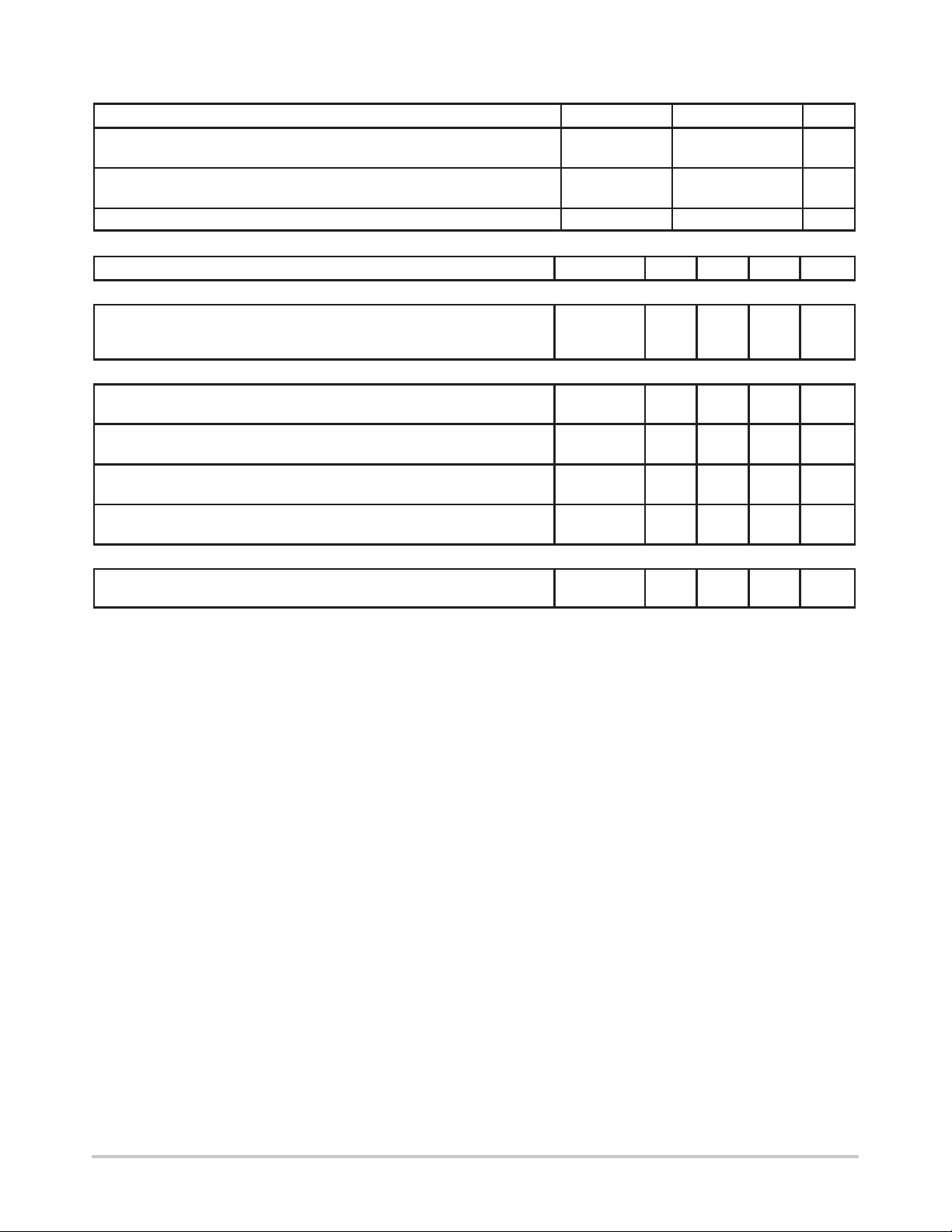
P ACKAGE DIMENSIONS
SOT–223
CASE 318E–04
ISSUE J
B
D
C
M
NOTES:
1. DIMENSIONING AND TOLERANCING PER ANSI
Y14.5M, 1982.
2. CONTROLLING DIMENSION: INCH.
INCHES
DIMAMIN MAX MIN MAX
0.249 0.263 6.30 6.70
B 0.130 0.145 3.30 3.70
C 0.060 0.068 1.50 1.75
D 0.024 0.035 0.60 0.89
F 0.115 0.126 2.90 3.20
G 0.087 0.094 2.20 2.40
H 0.0008 0.0040 0.020 0.100
J
J 0.009 0.014 0.24 0.35
K 0.060 0.078 1.50 2.00
L 0.033 0.041 0.85 1.05
M 0 10 0 10
____
S 0.264 0.287 6.70 7.30
MILLIMETERS
K
STYLE 10:
PIN 1. CATHODE
2. ANODE
3. GATE
4. ANODE
http://onsemi.com
9

Notes
MCR08B, MCR08M
http://onsemi.com
10

Notes
MCR08B, MCR08M
http://onsemi.com
11

MCR08B, MCR08M
ON Semiconductor and are trademarks of Semiconductor Components Industries, LLC (SCILLC). SCILLC reserves the right to make changes
without further notice to any products herein. SCILLC makes no warranty , representation or guarantee regarding the suitability of its products for any particular
purpose, nor does SCILLC assume any liability arising out of the application or use of any product or circuit, and specifically disclaims any and all liability ,
including without limitation special, consequential or incidental damages. “Typical” parameters which may be provided in SCILLC data sheets and/or
specifications can and do vary in different applications and actual performance may vary over time. All operating parameters, including “Typicals” must be
validated for each customer application by customer’s technical experts. SCILLC does not convey any license under its patent rights nor the rights of others.
SCILLC products are not designed, intended, or authorized for use as components in systems intended for surgical implant into the body, or other applications
intended to support or sustain life, or for any other application in which the failure of the SCILLC product could create a situation where personal injury or
death may occur. Should Buyer purchase or use SCILLC products for any such unintended or unauthorized application, Buyer shall indemnify and hold
SCILLC and its officers, employees, subsidiaries, affiliates, and distributors harmless against all claims, costs, damages, and expenses, and reasonable
attorney fees arising out of, directly or indirectly , any claim of personal injury or death associated with such unintended or unauthorized use, even if such claim
alleges that SCILLC was negligent regarding the design or manufacture of the part. SCILLC is an Equal Opportunity/Affirmative Action Employer .
PUBLICATION ORDERING INFORMATION
NORTH AMERICA Literature Fulfillment:
Literature Distribution Center for ON Semiconductor
P.O. Box 5163, Denver, Colorado 80217 USA
Phone: 303–675–2175 or 800–344–3860 Toll Free USA/Canada
Fax: 303–675–2176 or 800–344–3867 Toll Free USA/Canada
Email: ONlit@hibbertco.com
Fax Response Line: 303–675–2167 or 800–344–3810 T oll Free USA/Canada
N. American Technical Support: 800–282–9855 Toll Free USA/Canada
EUROPE: LDC for ON Semiconductor – European Support
German Phone: (+1) 303–308–7140 (M–F 1:00pm to 5:00pm Munich Time)
Email: ONlit–german@hibbertco.com
French Phone: (+1) 303–308–7141 (M–F 1:00pm to 5:00pm Toulouse Time)
Email: ONlit–french@hibbertco.com
English Phone: (+1) 303–308–7142 (M–F 12:00pm to 5:00pm UK Time)
Email: ONlit@hibbertco.com
EUROPEAN TOLL–FREE ACCESS*: 00–800–4422–3781
*Available from Germany, France, Italy, England, Ireland
CENTRAL/SOUTH AMERICA:
Spanish Phone: 303–308–7143 (Mon–Fri 8:00am to 5:00pm MST)
Email: ONlit–spanish@hibbertco.com
ASIA/PACIFIC : LDC for ON Semiconductor – Asia Support
Phone: 303–675–2121 (T ue–Fri 9:00am to 1:00pm, Hong Kong T ime)
T oll Free from Hong Kong & Singapore:
001–800–4422–3781
Email: ONlit–asia@hibbertco.com
JAPAN: ON Semiconductor, Japan Customer Focus Center
4–32–1 Nishi–Gotanda, Shinagawa–ku, T okyo, Japan 141–0031
Phone: 81–3–5740–2745
Email: r14525@onsemi.com
ON Semiconductor Website: http://onsemi.com
For additional information, please contact your local
Sales Representative.
http://onsemi.com
12
MCR08BT1/D
 Loading...