

MC74HC573A
Octal 3−State Noninverting
Transparent Latch
High−Performance Silicon−Gate CMOS
The MC74HC573A is identical in pinout to the LS573. The devices
are compatible with standard CMOS outputs; with pullup resistors,
they are compatible with LSTTL outputs.
These latches appear transparent to data (i.e., the outputs change
asynchronously) when Latch Enable is high. When Latch Enable goes
low, data meeting the setup and hold time becomes latched.
The HC573A is identical in function to the HC373A but has the data
inputs on the opposite side of the package from the outputs to facilitate
PC board layout.
Features
• Pb−Free Packages are Available*
• Output Drive Capability: 15 LSTTL Loads
• Outputs Directly Interface to CMOS, NMOS and TTL
• Operating Voltage Range: 2.0 to 6.0 V
• Low Input Current: 1.0 A
• In Compliance with the JEDEC Standard No. 7.0 A Requirements
• Chip Complexity: 218 FETs or 54.5 Equivalent Gates
http://onsemi.com
MARKING
DIAGRAMS
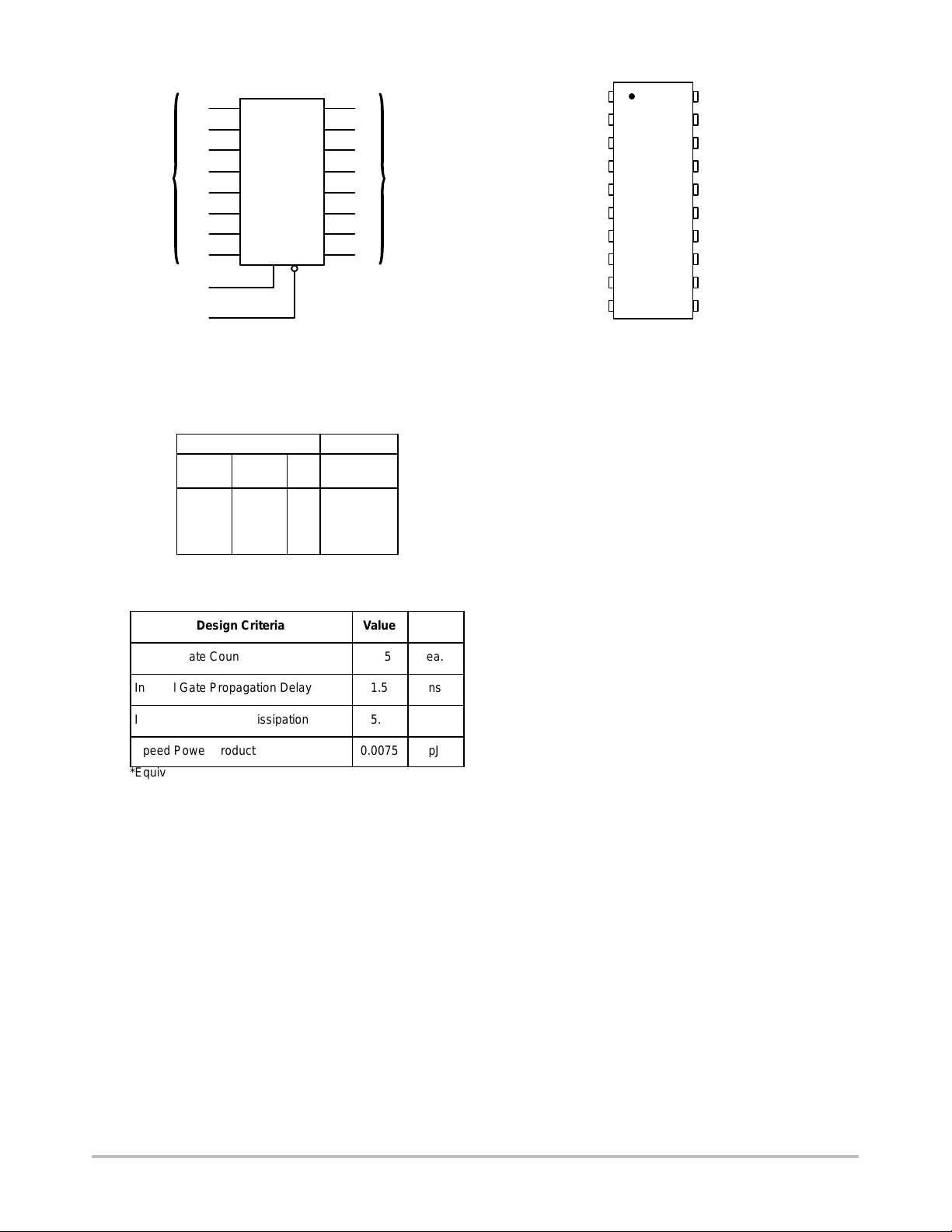
20
PDIP−20
N SUFFIX
20
1
20
1
20
1
CASE 738
SOIC WIDE−20
DW SUFFIX
CASE 751D
TSSOP−20
DT SUFFIX
CASE 948E
MC74HC573AN
AWLYYWW
1
20
HC573A
AWLYYWW
1
20
HC
573A
ALYW
1
*For additional information on our Pb−Free strategy and soldering details, please
download the ON Semiconductor Soldering and Mounting Techniques
Reference Manual, SOLDERRM/D.
Semiconductor Components Industries, LLC, 2004
December, 2004 − Rev. 10
1 Publication Order Number:
A = Assembly Location
WL = Wafer Lot
YY = Year
WW = Work Week
ORDERING INFORMATION
See detailed ordering and shipping information in the package
dimensions section on page 3 of this data sheet.
MC74HC573A/D
MC74HC573A
Î
Î
Î
Î
Î
Î
D0
D1
D2
DATA
INPUTS
D3
D4
D5
D6
D7
LATCH ENABLE
OUTPUT ENABLE
Figure 1. LOGIC DIAGRAM Figure 2. PIN ASSIGNMENT
Output Latch
Enable Enable D Q
X = Don’t Care
Z = High Impedance
219
3
4
5
6
7
8
9
Q0
18
Q1
17
Q2
16
15
14
13
12
Q3
Q4
Q5
Q6
Q7
NONINVERTING
OUTPUTS
11
1
PIN 20 = V
PIN 10 = GND
CC
FUNCTION TABLE
Inputs Output
LHHH
LHLL
L L X No Change
HXXZ
OUTPUT
ENABLE
GND
D0
D1
D2
D3 5
D4
D5
D6
D7
1
2
3
4
6
7
8
9
10
20
V
CC
19
Q0
18
Q1
17
Q2
16
Q3
15
Q4
14
Q5
13
Q6
12
Q7
LATCH
11
ENABLE
Design Criteria
Internal Gate Count*
ОООООООО
Internal Gate Propagation Delay
Internal Gate Power Dissipation
Speed Power Product
ОООООООО
*Equivalent to a two−input NAND gate.
Value
54.5
ÎÎ
1.5
5.0
0.0075
ÎÎ
Units
ea.
Î
ns
W
pJ
Î
http://onsemi.com
2
MC74HC573A
Î
Î
Î
Î
Î
Î
Î
Î
Î
ÎÎ
ÎÎ
ÎÎ
ÎÎ
Î
Î
Î
ÎÎ
ÎÎ
Î
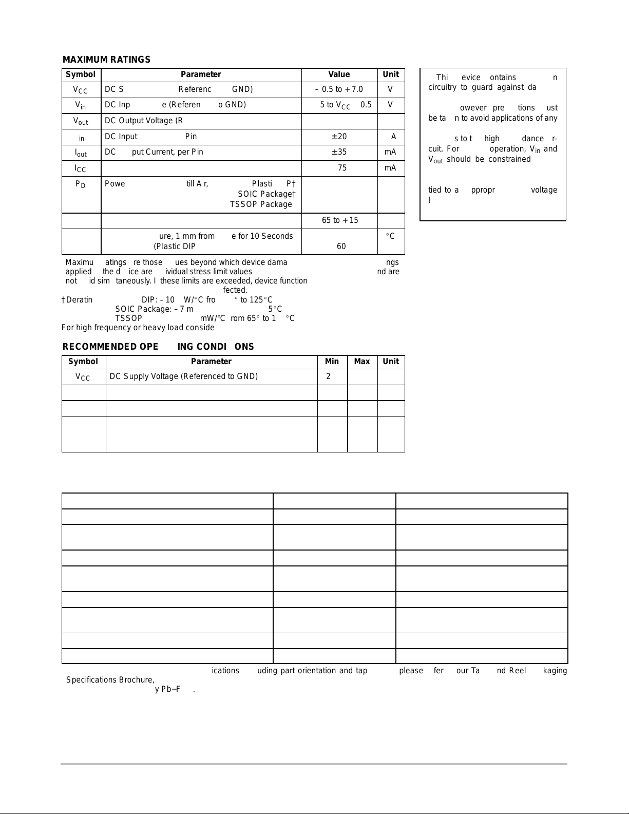
MAXIMUM RATINGS
Symbol
V
V
ÎÎ
ÎÎ
DC Supply Voltage (Referenced to GND)
CC
V
DC Input Voltage (Referenced to GND)
in
DC Output Voltage (Referenced to GND)
out
I
DC Input Current, per Pin
in
I
DC Output Current, per Pin
out
I
DC Supply Current, VCC and GND Pins
CC
P
Power Dissipation in Still Air, Plastic DIP†
D
ОООООООООООО
T
Storage Temperature
stg
T
Lead Temperature, 1 mm from Case for 10 Seconds
L
ОООООООООООО
Maximum ratings are those values beyond which device damage can occur. Maximum ratings
applied to the device are individual stress limit values (not normal operating conditions) and are
ООООООООООООООООООООО
not valid simultaneously. If these limits are exceeded, device functional operation is not implied,
damage may occur and reliability may be affected.
†Derating — Plastic DIP: –10 mW/C from 65 to 125C
SOIC Package: –7 mW/C from 65 to 125C
TSSOP Package: −6.1 mW/°C from 65 to 125C
For high frequency or heavy load considerations, see Chapter 2 of the ON Semiconductor High−Speed CMOS Data Book (DL129/D).
Parameter
SOIC Package†
TSSOP Package†
(Plastic DIP, TSSOP or SOIC Package)
Value
– 0.5 to + 7.0
– 0.5 to VCC + 0.5
– 0.5 to VCC + 0.5
± 20
± 35
± 75
750
500
ÎÎÎ
450
– 65 to + 150
260
ÎÎÎ
Unit
mA
mA
mA
mW
Î
C
C
Î
This device contains protection
V
V
V
circuitry to guard against damage
due to high static voltages or electric
fields. However, precautions must
be taken to avoid applications of any
voltage higher than maximum rated
voltages to this high−impedance circuit. For proper operation, V
V
should be constrained to the
out
range GND (V
in
or V
) VCC.
out
in
and
Unused inputs must always be
tied to an appropriate logic voltage
level (e.g., either GND or V
CC
Unused outputs must be left open.
).
RECOMMENDED OPERATING CONDITIONS
Symbol
V
CC
Vin, V
T
A
tr, t
ÎÎ
DC Supply Voltage (Referenced to GND)
DC Input Voltage, Output Voltage (Referenced to GND)
out
Operating Temperature, All Package Types
Input Rise and Fall Time VCC = 2.0 V
f
(Figure 1) V
ООООООООООООО
Parameter
V
= 4.5 V
CC
= 6.0 V
CC
Min
2.0
0
– 55
0
0
Î
0
Max
6.0
V
CC
+ 125
1000
500
400
Unit
V
V
C
ns
Î
ORDERING INFORMATION
Device Package Shipping
MC74HC573AN PDIP−20 1440 Units / Box
MC74HC573ANG PDIP−20
1440 Units / Box
(Pb−Free)
MC74HC573ADW SOIC−WIDE 38 Units / Rail
MC74HC573ADWG SOIC−WIDE
38 Units / Rail
(Pb−Free)
MC74HC573ADWR2 SOIC−WIDE 1000 Units / Reel
MC74HC573ADWR2G SOIC−WIDE
1000 Units / Reel
(Pb−Free)
MC74HC573ADT TSSOP−20* 75 Units / Rail
MC74HC573ADTR2 TSSOP−20* 2500 Units / Reel
†For information on tape and reel specifications, including part orientation and tape sizes, please refer to our Tape and Reel Packaging
Specifications Brochure, BRD8011/D.
*This package is inherently Pb−Free.
†
http://onsemi.com
3

MC74HC573A
V
CC
Î
Î
Î
Î
Î
Î
Î
Î
Î
Î
Î
Î
Î
Î
Î
Î
Î
Î
Î
Î
Î
Î
Î
Î
Î
Î
Î
Î
Î
Î
Î
Î
Î
Î
Î
Î
Î
Î
Î
Î
Î
Î
Î
Î
Î
Î
Î
Î
Î
Î
Î
Î
Î
Î
Î
Î
Î
Î
Î
V
CC
Î
Î
Î
Î
Î
Î
Î
Î
Î
Î
Î
Î
Î
Î
Î
Î
Î
Î
Î
Î
Î
Î
Î
Î
Î
Î
Î
Î
Î
Î
Î
Î
Î
Î
Î
Î
Î
Î
Î
Î
Î
Î
Î
Î
Î
Î
Î
Î
Î
Î
Î
Î
Î
Î
Î
Î
Î
Î
Î
DC ELECTRICAL CHARACTERISTICS (Voltages Referenced to GND)
V
– 55 to 25C
2.0
3.0
Î
4.5
Î
6.0
2.0
3.0
Î
4.5
V
ÎÎÎ
ÎÎÎ
ÎÎÎ
Symbol
V
IH
ÎÎ
ÎÎ
V
IL
ÎÎ
Parameter
Minimum High−Level Input
Voltage
ООООООО
ООООООО
Maximum Low−Level Input
Voltage
ООООООО
Test Conditions
V
= 0.1 V or VCC – 0.1 V
out
| 20 A
|I
ООООООО
out
ООООООО
V
= 0.1 V or VCC – 0.1 V
out
| 20 A
|I
out
ООООООО
6.0
V
ÎÎ
ÎÎÎОООООООÎООООООО
V
ÎÎ
ÎÎÎОООООООÎООООООО
ÎÎ
ÎÎ
Minimum High−Level Output
OH
OL
I
in
I
OZ
I
CC
ООООООО
Voltage
Maximum Low−Level Output
ООООООО
Voltage
Maximum Input Leakage Current
Maximum Three−State
Leakage Current
ООООООО
Maximum Quiescent Supply
Current (per Package)
ООООООО
Vin = VIH or V
ООООООО
|I
| 20 A
out
Vin = VIH or V
V
= 0.1 V or VCC – 0.1 V
out
ООООООО
| 20 A
|I
out
Vin = VIH or V
IL
|I
out
| 6.0 mA
|I
out
|I
| 7.8 mA
out
|I
out
|I
| 6.0 mA
out
| 7.8 mA
|I
out
| ≤ 2.4mA
| ≤ 2.4mA
IL
IL
Vin = VCC or GND
Output in High−Impedance State
V
= VIL or V
ООООООО
in
V
= VCC or GND
out
IH
Vin = VCC or GND
I = 0 A
II
ООООООО
out
2.0
Î
4.5
6.0
3.0
Î
4.5
6.0
2.0
Î
4.5
6.0
3.0
Î
4.5
6.0
6.0
6.0
Î
6.0
Î
ÎÎÎ
ÎÎÎ
ÎÎÎ
ÎÎÎ
ÎÎÎ
ÎÎÎ
NOTE:Information on typical parametric values can be found i n Chapter 2 of the ON S emiconductor High−Speed CMOS Data Book ( DL129/D).
Guaranteed Limit
1.5
2.1
3.15
4.2
0.5
0.9
1.35
1.8
1.9
4.4
5.9
2.48
3.98
5.48
0.1
0.1
0.1
0.26
0.26
0.26
± 0.1
– 0.5
4.0
85C
1.5
2.1
ÎÎ
3.15
ÎÎ
4.2
0.5
0.9
ÎÎ
1.35
1 8
1.9
ÎÎ
4.4
5.9
2.34
ÎÎ
3.84
5.34
0.1
ÎÎ
0.1
0.1
0.33
ÎÎ
0.33
0.33
± 1.0
– 5.0
ÎÎ
40
ÎÎ
125C
1.5
2.1
ÎÎ
3.15
ÎÎ
4.2
0.5
0.9
ÎÎ
1.35
1.8
1.9
ÎÎ
4.4
5.9
2.2
ÎÎ
3.7
5.2
0.1
ÎÎ
0.1
0.1
0.4
ÎÎ
0.4
0.4
± 1.0
– 10
ÎÎ
160
ÎÎ
Unit
V
V
V
V
A
A
A
AC ELECTRICAL CHARACTERISTICS (C
Symbol
t
PLH
t
PHL
ÎÎ
ÎÎ
t
PLH
t
PHL
ÎÎ
ÎÎ
t
PLZ
t
PHZ
ÎÎ
t
PZL
t
ÎÎ
PZH
ÎÎ
t
TLH
t
THL
ÎÎ
ÎÎ
C
in
C
out
ÎÎ
,
Maximum Propagation Delay, Input D to Q
(Figures 1 and 5)
ООООООООООООООО
ООООООООООООООО
,
Maximum Propagation Delay, Latch Enable to Q
(Figures 2 and 5)
ООООООООООООООО
ООООООООООООООО
,
Maximum Propagation Delay, Output Enable to Q
(Figures 3 and 6)
ООООООООООООООО
,
Maximum Propagation Delay, Output Enable to Q
(Figures 3 and 6)
ООООООООООООООО
ООООООООООООООО
,
Maximum Output Transition Time, Any Output
(Figures 1 and 5)
ООООООООООООООО
ООООООООООООООО
Maximum Input Capacitance
Maximum Three−State Output Capacitance (Output in High−Impedance
ООООООООООООООООО
State)
Parameter
= 50 pF, Input tr = tf = 6.0 ns)
L
V
2.0
3.0
Î
4.5
Î
6.0
2.0
3.0
Î
4.5
6.0
Î
2.0
3.0
4.5
Î
6.0
2.0
3.0
Î
4.5
Î
6.0
2.0
3.0
Î
4.5
6.0
Î
V
Guaranteed Limit
– 55 to 25C
150
100
ÎÎÎ
30
ÎÎÎ
26
160
105
ÎÎÎ
32
27
ÎÎÎ
150
100
30
ÎÎÎ
26
150
100
ÎÎÎ
30
ÎÎÎ
26
60
27
ÎÎÎ
12
10
ÎÎÎ
10
15
ÎÎÎ
85C
190
140
ÎÎ
38
ÎÎ
33
200
145
ÎÎ
40
34
ÎÎ
190
125
38
ÎÎ
33
190
125
ÎÎ
38
ÎÎ
33
75
32
ÎÎ
15
13
ÎÎ
10
15
ÎÎ
125C
225
180
ÎÎ
45
ÎÎ
38
240
190
ÎÎ
48
41
ÎÎ
225
150
45
ÎÎ
38
225
150
ÎÎ
45
ÎÎ
38
90
36
ÎÎ
18
15
ÎÎ
10
15
ÎÎ
Unit
ns
ns
ns
ns
ns
pF
pF
NOTE: For propagation delays with loads other than 50 pF, and information on typical parametric values, see Chapter 2 of the ON
Semiconductor High−Speed CMOS Data Book (DL129/D).
Typical @ 25°C, VCC = 5.0 V
C
PD
Power Dissipation Capacitance (Per Enabled Output)*
*Used to d etermine the no−load dynamic power consumption: PD = CPD V
2
f + ICC VCC. For load considerations, see Chapter 2 of t h e
CC
23
pF
ON Semiconductor High−Speed CMOS Data Book (DL129/D).
http://onsemi.com
4

MC74HC573A
V
Î
Î
Î
Î
Î
Î
Î
Î
Î
Î
Î
Î
Î
Î
Î
Î
Î
Î
Î
Î
Î
Î
Î
Î
Î
Î
Î
Î
Î
Î
Î
Î
Î
Î
Î
Î
Î
Î
Î
Î
Î
Î
Î
Î
Î
Î
Î
Î
Î
Î
Î
Î
Î
Î
Î
Î
Î
Î
Î
Î
Î
Î
Î
Î
Î
Î
Î
Î
Î
Î
Î
Î
Î
Î
Î
Î
Î
Î
Î
Î
TIMING REQUIREMENTS (C
Symbol
t
su
ÎÎ
ÎÎ
t
h
ÎÎ
ÎÎ
t
w
ÎÎ
ÎÎ
tr, t
f
ÎÎ
ÎÎ
Minimum Setup Time, Input D to Latch Enable
ООООООООООО
ООООООООООО
Minimum Hold Time, Latch Enable to Input D
ООООООООООО
ООООООООООО
Minimum Pulse Width, Latch Enable
ООООООООООО
ООООООООООО
Maximum Input Rise and Fall Times
ООООООООООО
ООООООООООО
Parameter
= 50 pF, Input tr = tf = 6.0 ns)
L
Fig.
4
Î
Î
4
Î
Î
2
Î
Î
1
Î
Î
CC
V
2.0
Î
3.0
4.5
Î
6.0
2.0
Î
3.0
4.5
Î
6.0
2.0
Î
3.0
4.5
Î
6.0
2.0
Î
3.0
4.5
Î
6.0
– 55 to 25C
Min
Max
50
Î
Î
40
10
Î
Î
9.0
5.0
Î
5.0
5.0
Î
5.0
Î
Î
75
60
15
13
Î
Î
Î
Î
1000
Î
Î
Î
800
500
Î
400
Guaranteed Limit
85C
Min
Max
65
Î
50
13
Î
Î
Î
11
5.0
Î
5.0
5.0
Î
5.0
95
Î
80
19
Î
16
Î
Î
Î
Î
1000
Î
Î
Î
800
500
Î
400
125C
Min
75
Î
60
15
Î
13
5.0
Î
5.0
5.0
Î
5.0
110
Î
90
22
Î
19
Î
Î
Max
Î
Î
Î
Î
Î
Î
1000
Î
800
500
Î
400
Unit
ns
ns
ns
ns
http://onsemi.com
5

INPUT D
MC74HC573A
SWITCHING WAVEFORMS
V
t
r
90%
50%
10%
t
PLH
Q
90%
50%
10%
t
TLH
t
f
V
CC
GND
t
PHL
t
THL
LATCH
ENABLE
Q
50%
50%
t
w
t
PLH
t
PHL
Figure 3. Figure 4.
CC
GND
OUTPUT
ENABLE
DEVICE
UNDER
TEST
50%
t
PZLtPLZ
Q
Q
50%
t
PZHtPHZ
1.3 V
Figure 5. Figure 6.
TEST POINT
OUTPUT
DEVICE
UNDER
TEST
CL*
*Includes all probe and jig capacitance
Figure 7. Test Circuit
TEST POINT
OUTPUT
1 k
CL*
CONNECT TO VCC WHEN
TESTING t
CONNECT TO GND WHEN
TESTING t
10%
90%
PLZ
PHZ
3.0 V
GND
HIGH
IMPEDANCE
V
V
HIGH
IMPEDANCE
AND t
AND t
OL
OH
PZL
PZH
VALID
INPUT D
LATCH
50%
t
SU
t
h
50%
ENABLE
2
D0
3
D1
4
D2
5
D3
6
D4
7
D5
8
D6
9
.
D7
D
LE
D
LE
D
LE
D
LE
D
LE
D
LE
D
LE
D
LE
Q
Q
Q
Q
Q
Q
Q
Q
V
CC
GND
V
CC
GND
19
Q0
18
Q1
17
Q2
16
Q3
15
Q4
14
Q5
13
Q6
12
Q7
.
LATCH ENABLE
11
1
*Includes all probe and jig capacitance
OUTPUT ENABLE
Figure 8. Test Circuit Figure 9. EXPANDED LOGIC DIAGRAM
http://onsemi.com
6
MC74HC573A
PACKAGE DIMENSIONS
PDIP−20
N SUFFIX
PLASTIC DIP PACKAGE
CASE 738−03
ISSUE E
−T−
SEATING
PLANE
−A−
20
11
B
1
10
C
L
K
M
E
FG
N
20 PL
D
0.25 (0.010) T
J 20 PL
M
M
A
0.25 (0.010) T
M
NOTES:
1. DIMENSIONING AND TOLERANCING PER ANSI
Y14.5M, 1982.
2. CONTROLLING DIMENSION: INCH.
3. DIMENSION L TO CENTER OF LEAD WHEN
FORMED PARALLEL.
4. DIMENSION B DOES NOT INCLUDE MOLD
FLASH.
DIM MIN MAX MIN MAX
A 25.66 27.171.010 1.070
B 6.10 6.600.240 0.260
C 3.81 4.570.150 0.180
D 0.39 0.550.015 0.022
E
F
G 2.54 BSC0.100 BSC
J 0.21 0.380.008 0.015
K 2.80 3.550.110 0.140
L 7.62 BSC0.300 BSC
M 0 15 0 15
N 0.51 1.010.020 0.040
M
B
MILLIMETERSINCHES
1.27 BSC0.050 BSC
1.27 1.770.050 0.070
SOIC−20
DW SUFFIX
CASE 751D−05
ISSUE G
H10X
M
B
M
0.25
D
20
A
11
E
1
B20X
M
0.25
T
SAS
B
10
B
h X 45
A
L
18X
SEATING
e
A1
T
PLANE
C
NOTES:
1. DIMENSIONS ARE IN MILLIMETERS.
2. INTERPRET DIMENSIONS AND TOLERANCES
PER ASME Y14.5M, 1994.
3. DIMENSIONS D AND E DO NOT INCLUDE MOLD
PROTRUSION.
4. MAXIMUM MOLD PROTRUSION 0.15 PER SIDE.
5. DIMENSION B DOES NOT INCLUDE DAMBAR
PROTRUSION. ALLOWABLE PROTRUSION
SHALL BE 0.13 TOTAL IN EXCESS OF B
DIMENSION AT MAXIMUM MATERIAL
CONDITION.
MILLIMETERS
DIM MIN MAX
A 2.35 2.65
A1 0.10 0.25
B 0.35 0.49
C 0.23 0.32
D 12.65 12.95
E 7.40 7.60
e 1.27 BSC
H 10.05 10.55
h 0.25 0.75
L 0.50 0.90
0 7
http://onsemi.com
7

MC74HC573A
PACKAGE DIMENSIONS
TSSOP−20
DT SUFFIX
CASE 948E−02
ISSUE B
20X REFK
S
U0.15 (0.006) T
0.10 (0.004) V
M
S
U
T
S
K
2X
L/2
L
PIN 1
IDENT
110
1120
B
JJ1
−U−
N
S
U0.15 (0.006) T
A
K1
SECTION N−N
0.25 (0.010)
M
−V−
N
F
DETAIL E
C
G
H
DETAIL E
0.100 (0.004)
−T−
SEATING
PLANE
D
NOTES:
1. DIMENSIONING AND TOLERANCING
PER ANSI Y14.5M, 1982.
2. CONTROLLING DIMENSION:
MILLIMETER.
3. DIMENSION A DOES NOT INCLUDE
MOLD FLASH, PROTRUSIONS OR GATE
BURRS. MOLD FLASH OR GATE BURRS
SHALL NOT EXCEED 0.15 (0.006) PER
SIDE.
4. DIMENSION B DOES NOT INCLUDE
INTERLEAD FLASH OR PROTRUSION.
INTERLEAD FLASH OR PROTRUSION
SHALL NOT EXCEED 0.25 (0.010) PER
SIDE.
5. DIMENSION K DOES NOT INCLUDE
DAMBAR PROTRUSION. ALLOWABLE
DAMBAR PROTRUSION SHALL BE 0.08
(0.003) TOTAL IN EXCESS OF THE K
DIMENSION AT MAXIMUM MATERIAL
CONDITION.
6. TERMINAL NUMBERS ARE SHOWN
FOR REFERENCE ONLY.
7. DIMENSION A AND B ARE TO BE
DETERMINED AT DATUM PLANE −W−.
MILLIMETERS
−W−
DIMAMIN MAX MIN MAX
B 4.30 4.50 0.169 0.177
C 1.20 0.047
D 0.05 0.15 0.002 0.006
F 0.50 0.75 0.020 0.030
G 0.65 BSC 0.026 BSC
H 0.27 0.37 0.011 0.015
J 0.09 0.20 0.004 0.008
J1 0.09 0.16 0.004 0.006
K 0.19 0.30 0.007 0.012
K1 0.19 0.25 0.007 0.010
L 6.40 BSC 0.252 BSC
M 0 8 0 8
6.60 0.260
6.40 0.252
−−− −−−
INCHES
ON Semiconductor and are registered trademarks of Semiconductor Components Industries, LLC (SCILLC). SCILLC reserves the right to make changes without further notice
to any products herein. SCILLC makes no warranty, representation or guarantee regarding the suitability of its products for any particular purpose, nor does SCILLC assume any liability
arising out of the application or use of any product or circuit, and specifically disclaims any and all liability, including without limitation special, consequential or incidental damages.
“Typical” parameters which may be provided in SCILLC data sheets and/or specifications can and do vary in different applications and actual performance may vary over time. All
operating parameters, including “Typicals” must be validated for each customer application by customer’s technical experts. SCILLC does not convey any license under its patent rights
nor the rights of others. SCILLC products are not designed, intended, or authorized for use as components in systems intended for surgical implant into the body, or other applications
intended to support or sustain life, or for any other application in which the failure of the SCILLC product could create a situation where personal injury or death may occur. Should
Buyer purchase or use SCILLC products for any such unintended or unauthorized application, Buyer shall indemnify and hold SCILLC and its officers, employees, subsidiaries, affiliates,
and distributors harmless against all claims, costs, damages, and expenses, and reasonable attorney fees arising out of, directly or indirectly, any claim of personal injury or death
associated with such unintended or unauthorized use, even if such claim alleges that SCILLC was negligent regarding the design or manufacture of the part. SCILLC is an Equal
Opportunity/Affirmative Action Employer. This literature is subject to all applicable copyright laws and is not for resale in any manner.
PUBLICATION ORDERING INFORMATION
LITERATURE FULFILLMENT:
Literature Distribution Center for ON Semiconductor
P.O. Box 61312, Phoenix, Arizona 85082−1312 USA
Phone: 480−829−7710 or 800−344−3860 Toll Free USA/Canada
Fax: 480−829−7709 or 800−344−3867 Toll Free USA/Canada
Email: orderlit@onsemi.com
N. American Technical Support: 800−282−9855 Toll Free
USA/Canada
Japan: ON Semiconductor, Japan Customer Focus Center
2−9−1 Kamimeguro, Meguro−ku, Tokyo, Japan 153−0051
Phone: 81−3−5773−3850
http://onsemi.com
ON Semiconductor Website: http://onsemi.com
Order Literature: http://www.onsemi.com/litorder
For additional information, please contact your
local Sales Representative.
MC74HC573A/D
8
 Loading...