

MC74HC4066A
Quad Analog Switch/
Multiplexer/Demultiplexer
High−Performance Silicon−Gate CMOS
The MC74HC4066A utilizes silicon−gate CMOS technology to
achieve fast propagation delays, low ON resistances, and low
OFF−channel leakage current. This bilateral switch/
multiplexer/demultiplexer controls analog and digital voltages that
may vary across the full power−supply range (from V
to GND).
CC
The HC4066A is identical in pinout to the metal−gate CMOS
MC14016 and MC14066. Each device has four independent switches.
The device has been designed so the ON resistances (R
linear over input voltage than R
of metal−gate CMOS analog
ON
) are more
ON
switches.
The ON/OFF control inputs are compatible with standard CMOS
outputs; with pullup resistors, they are compatible with LSTTL outputs.
For analog switches with voltage−level translators, see the HC4316A.
Features
• Fast Switching and Propagation Speeds
• High ON/OFF Output Voltage Ratio
• Low Crosstalk Between Switches
• Diode Protection on All Inputs/Outputs
• Wide Power−Supply Voltage Range (V
• Analog Input Voltage Range (V
CC
− GND) = 2.0 to 12.0 Volts
CC
− GND) = 2.0 to 12.0 Volts
• Improved Linearity and Lower ON Resistance over Input Voltage
than the MC14016 or MC14066
• Low Noise
• Chip Complexity: 44 FETs or 11 Equivalent Gates
• Pb−Free Packages are Available*
http://onsemi.com
MARKING
DIAGRAMS
14
PDIP−14
4
1
14
1
14
1
14
1
N SUFFIX
CASE 646
SOIC−14
D SUFFIX
CASE 751A
TSSOP−14
DT SUFFIX
CASE 948G
SOEIAJ−14
F SUFFIX
CASE 965
MC74HC4066AN
AWLYYWWG
1
14
HC4066AG
AWLYWW
1
14
HC40
66A
ALYW
1
14
74HC4066A
ALYWG
1
*For additional information on our Pb−Free strategy and soldering details, please
download the ON Semiconductor Soldering and Mounting Techniques
Reference Manual, SOLDERRM/D.
© Semiconductor Components Industries, LLC, 2005
June, 2005 − Rev. 7
1 Publication Order Number:
A = Assembly Location
L, WL = Wafer Lot
Y, YY = Year
W, WW = Work Week
G or = Pb−Free Package
(Note: Microdot may be in either location)
ORDERING INFORMATION
See detailed ordering and shipping information in the package
dimensions section on page 2 of this data sheet.
MC74HC4066A/D
MC74HC4066A
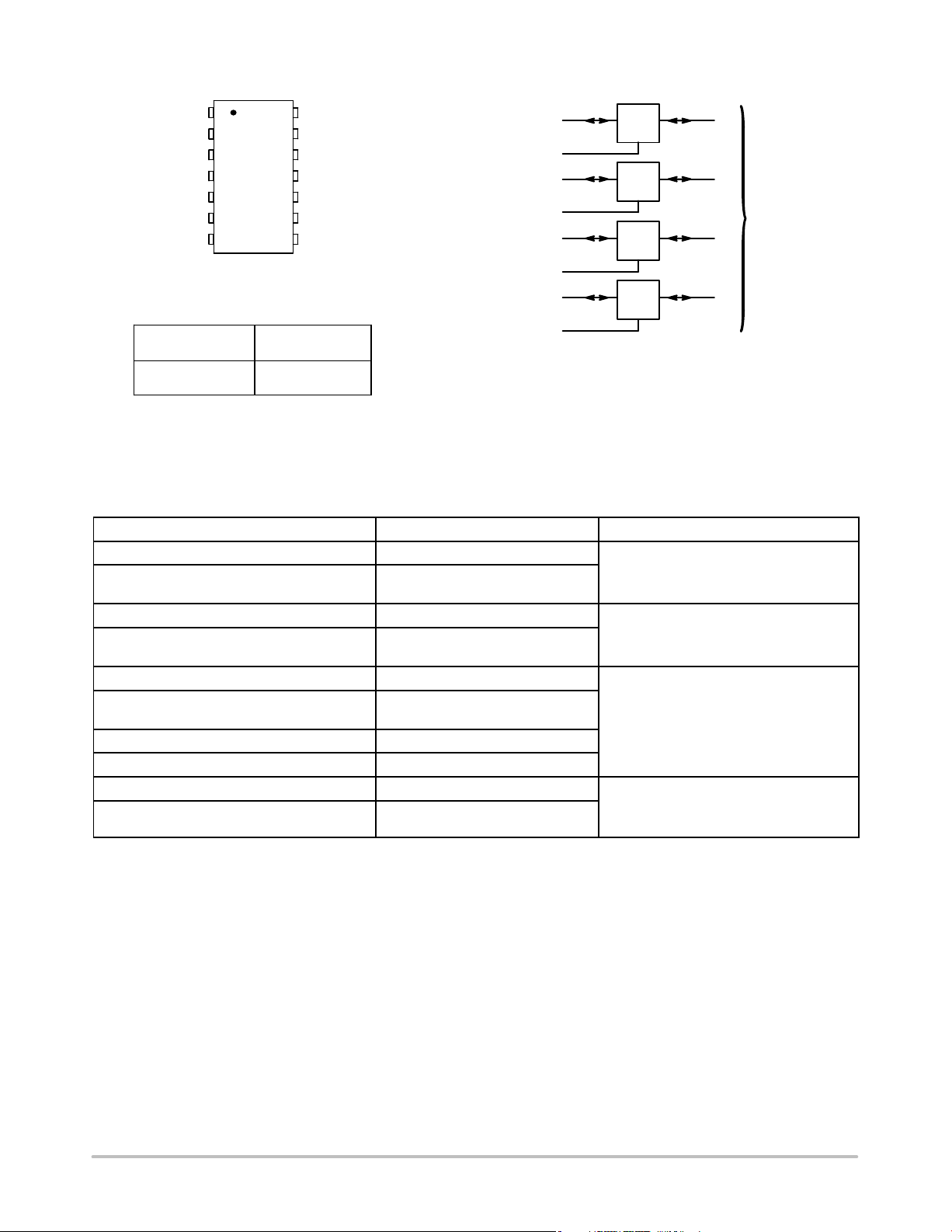
LOGIC DIAGRAM
PIN ASSIGNMENT
X
Y
Y
X
B ON/OFF CONTROL
C ON/OFF CONTROL
GND
On/Off Control State of
Input Analog Switch
1
A
2
A
3
B
4
B
6
7
V
14
CC
A ON/OFF CONTROL
13
D ON/OFF CONTROL
12
11
X
D
Y
105
D
9
Y
C
8
X
C
FUNCTION TABLE
LOff
HOn
A ON/OFF CONTROL
B ON/OFF CONTROL
C ON/OFF CONTROL
D ON/OFF CONTROL
1 2
X
A
13
4 3
X
B
5
8 9
X
C
6
11 10
X
D
12
ANALOG INPUTS/OUTPUTS = XA, XB, XC, X
PIN 14 = V
PIN 7 = GND
CC
Y
A
Y
B
ANALOG
OUTPUTS/INPUTS
Y
C
Y
D
D
ORDERING INFORMATION
Device Package Shipping
MC74HC4066AN PDIP−14
MC74HC4066ANG PDIP−14
500 Units / Rail
(Pb−Free)
MC74HC4066AD SOIC−14
MC74HC4066ADG SOIC−14
55 Units / Rail
(Pb−Free)
MC74HC4066ADR2 SOIC−14
MC74HC4066ADR2G SOIC−14
(Pb−Free)
2500 Tape & Reel
MC74HC4066ADTR2 TSSOP−14*
MC74HC4066ADTR2G TSSOP−14*
MC74HC4066AFEL SOEIAJ−14
MC74HC4066AFELG SOEIAJ−14
2000 Tape & Reel
(Pb−Free)
†For information on tape and reel specifications, including part orientation and tape sizes, please refer to our Tape and Reel Packaging
Specifications Brochure, BRD8011/D.
*This package is inherently Pb−Free.
†
http://onsemi.com
2
MC74HC4066A
Î
Î
Î
Î
Î
Î
Î
Î
Î
Î
Î
Î
Î
Î
Î
Î
Î
Î
Î
Î
Î
Î
Î
Î
Î
Î
Î
Î
Î
Î
l
Î
Î
Î
Î
Î
Î
Î
Î
Î
Î
Î
Î
Î
Î
Î
Î
Î
Î
Î
Î
Î
Î
Î
Î
Î
Î
Î
Î
Î
Î
Î
Î
Î
Î
Î
Î
Î
Î
Î
Î
Î
Î
Î
Î
Î
Î
Î
Î
Î
Î
Î
Î
Î
Î
Î
Î
Î
Î
Î
Î
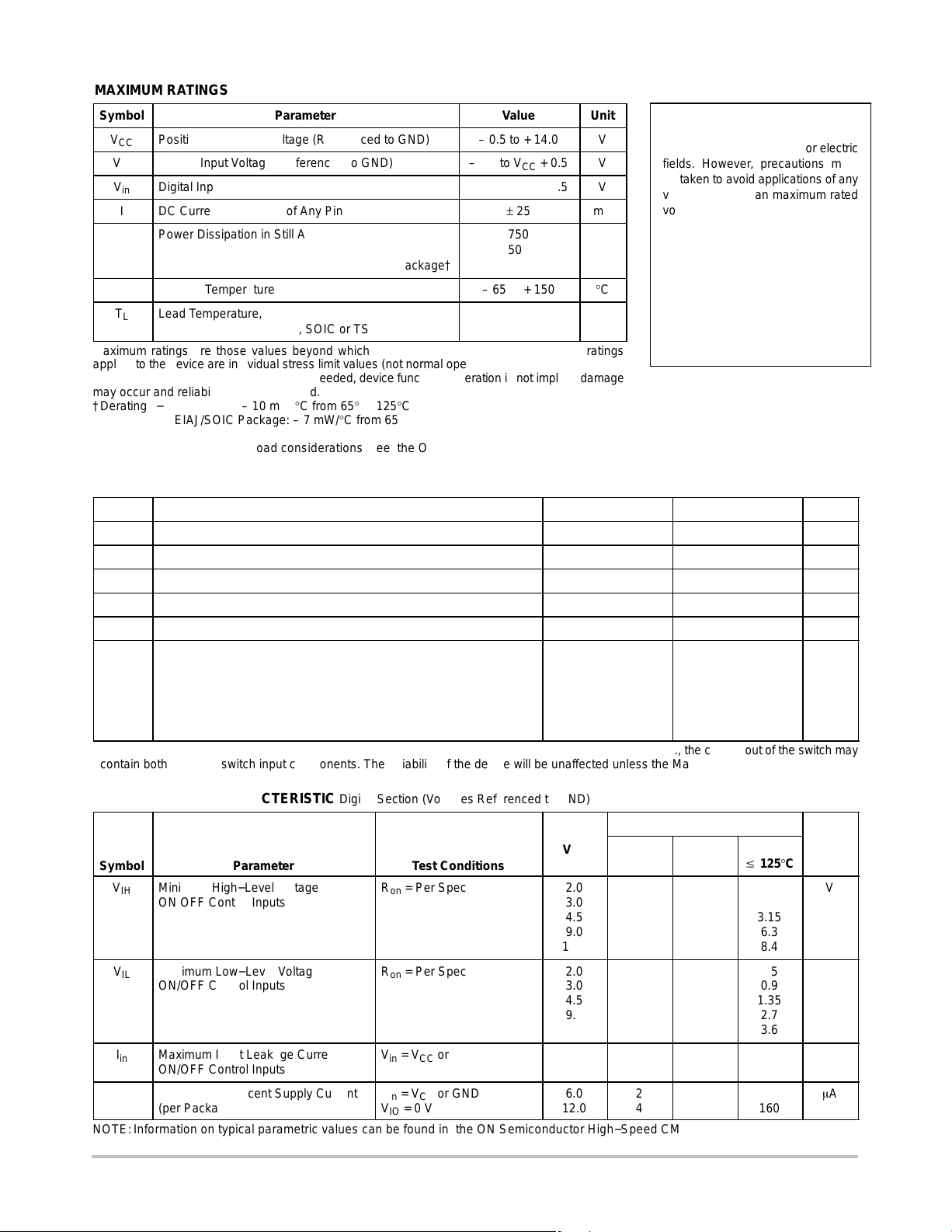
MAXIMUM RATINGS
Symbol
V
ÎÎ
ÎÎ
Positive DC Supply Voltage (Referenced to GND)
CC
V
Analog Input Voltage (Referenced to GND)
IS
V
Digital Input Voltage (Referenced to GND)
in
I
DC Current Into or Out of Any Pin
P
Power Dissipation in Still Air, Plastic DIP†
D
ОООООООООООО
T
Storage Temperature
stg
T
Lead Temperature, 1 mm from Case for 10 Seconds
L
ОООООООООООО
Maximum ratings are those values beyond which device damage can occur. Maximum ratings
applied to the device are individual stress limit values (not normal operating conditions) and are not
valid simultaneously. I f these limits are exceeded, device functional operation is not implied, damage
may occur and reliability may be affected.
†Derating − Plastic DIP: – 10 mW/°C from 65° to 125°C
EIAJ/SOIC Package: – 7 mW/°C from 65° to 125°C
TSSOP Package: − 6.1 mW/°C from 65° to 125°C
For high frequency or heavy load considerations, see the ON Semiconductor High−Speed CMOS Data Book (DL129/D).
RECOMMENDED OPERATING CONDITIONS
Symbol
V
VIO*
ÎÎ
ÎÎ
ÎÎ
ÎÎ
*For voltage drops across the switch greater than 1.2 V (switch on), excessive VCC current may be drawn; i.e., the current out of the switch may
contain both V
Positive DC Supply Voltage (Referenced to GND)
CC
V
Analog Input Voltage (Referenced to GND)
IS
V
Digital Input Voltage (Referenced to GND)
in
Static or Dynamic Voltage Across Switch
T
Operating Temperature, All Package Types
A
tr, t
Input Rise and Fall Time, ON/OFF Control
f
ООООООООООООООО
Inputs (Figure 10) V
ООООООООООООООО
ООООООООООООООО
ООООООООООООООО
and switch input components. The reliability of the device will be unaffected unless the Maximum Ratings are exceeded.
CC
Parameter
EIAJ/SOIC Package†
TSSOP Package†
(Plastic DIP, SOIC or TSSOP Package)
Parameter
Value
– 0.5 to + 14.0
– 0.5 to VCC + 0.5
– 0.5 to VCC + 0.5
± 25
750
500
ÎÎÎÎ
450
– 65 to + 150
260
ÎÎÎÎ
= 2.0 V
CC
= 3.0 V
V
CC
V
= 4.5 V
CC
V
= 9.0 V
CC
V
= 12.0 V
CC
Unit
V
V
V
mA
mW
Î
°C
°C
Î
Min
2.0
GND
GND
−
–55
ООООО
ООООО
ООООО
ООООО
0
0
0
0
0
This device contains protection
circuitry to guard against damage
due to high static voltages or electric
fields. However, precautions must
be taken to avoid applications of any
voltage higher than maximum rated
voltages to this high−impedance circuit. For proper operation, V
should be constrained to the
V
out
range GND v (V
in
or V
) v VCC.
out
in
and
Unused inputs must always be
tied to an appropriate logic voltage
level (e.g., either GND or V
CC
Unused outputs must be left open.
I/O pins must be connected to a
properly terminated line or bus.
Max
12.0
V
CC
V
CC
1.2
+ 125
ÎÎÎÎ
1000
600
ÎÎÎÎ
500
ÎÎÎÎ
400
250
ÎÎÎÎ
Unit
Î
Î
Î
Î
V
V
V
V
°C
ns
).
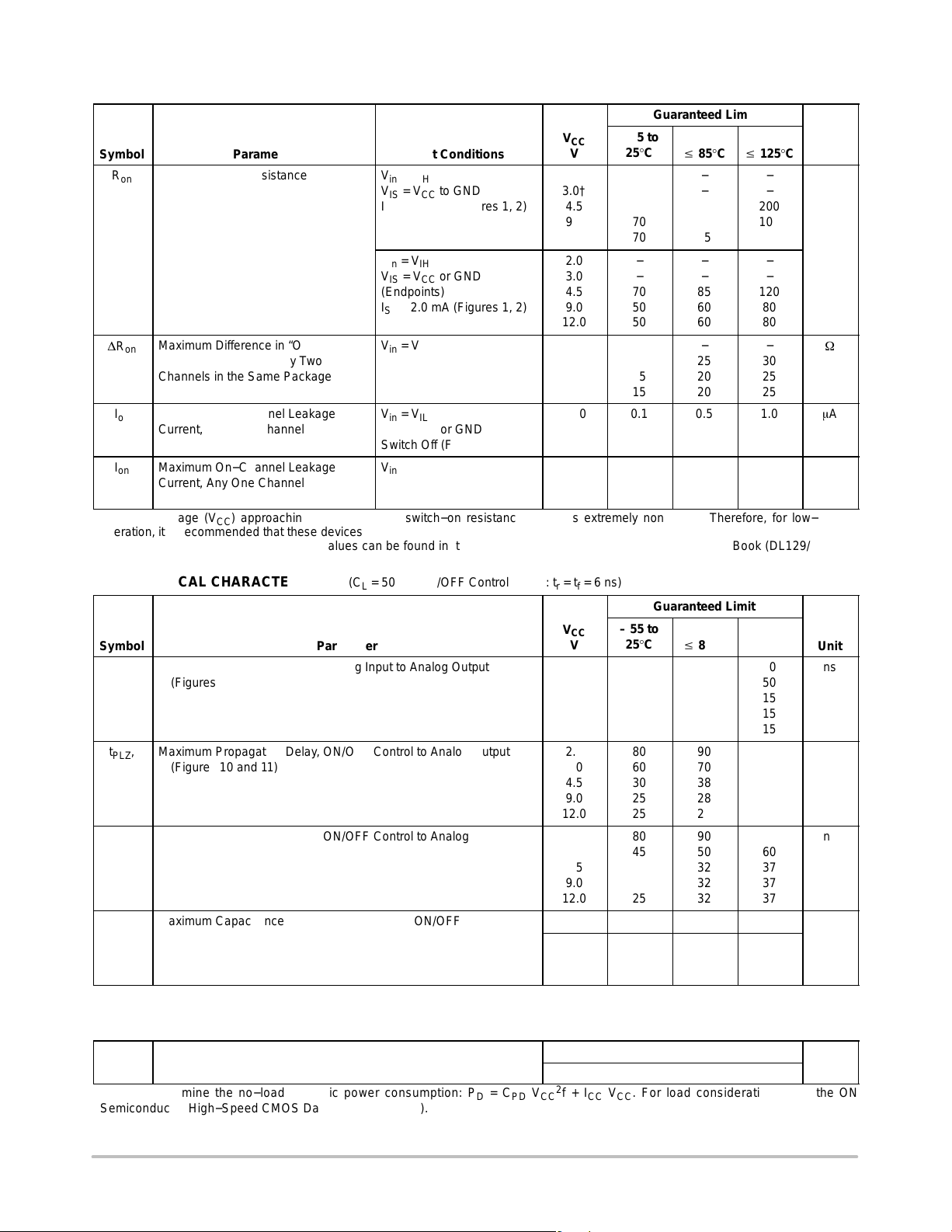
DC ELECTRICAL CHARACTERISTIC Digital Section (Voltages Referenced to GND)
ÎÎ
ÎÎ
Symbo
V
IH
ÎÎ
ÎÎ
ÎÎ
V
ÎÎ
ÎÎ
I
in
ÎÎ
I
CC
ОООООООО
ОООООООО
Parameter
Minimum High−Level Voltage
ON/OFF Control Inputs
ОООООООО
ОООООООО
ОООООООО
Maximum Low−Level Voltage
IL
ON/OFF Control Inputs
ОООООООО
ОООООООО
Maximum Input Leakage Current
ON/OFF Control Inputs
ОООООООО
Maximum Quiescent Supply Current
(per Package)
ОООООО
ОООООО
Test Conditions
Ron = Per Spec
ОООООО
ОООООО
ОООООО
Ron = Per Spec
ОООООО
ОООООО
Vin = VCC or GND
ОООООО
Vin = VCC or GND
= 0 V
V
IO
ÎÎ
V
CC
ÎÎ
V
2.0
3.0
ÎÎ
4.5
ÎÎ
9.0
12.0
ÎÎ
2.0
3.0
ÎÎ
4.5
9.0
ÎÎ
12.0
12.0
ÎÎ
6.0
12.0
NOTE:Information on typical parametric values can be found in the ON Semiconductor High−Speed CMOS Data Book (DL129/D).
http://onsemi.com
3
Guaranteed Limit
ООООООО
– 55 to
ÎÎ
25°C
1.5
2.1
ÎÎ
3.15
ÎÎ
6.3
8.4
ÎÎ
0.5
0.9
ÎÎ
1.35
2.7
ÎÎ
3.6
± 0.1
ÎÎ
2
4
Î
v 85°C
1.5
2.1
Î
3.15
Î
6.3
8.4
Î
0.5
0.9
Î
1.35
2.7
Î
3.6
± 1.0
Î
20
40
ÎÎ
v 125°C
1.5
2.1
ÎÎ
3.15
ÎÎ
6.3
8.4
ÎÎ
0.5
0.9
ÎÎ
1.35
2.7
ÎÎ
3.6
± 1.0
ÎÎ
40
160
Î
Î
Unit
Î
Î
Î
Î
Î
Î
V
V
A
A
MC74HC4066A
Î
l
Î
Î
Î
Î
Î
Î
Î
Î
Î
Î
Î
Î
Î
Î
Î
Î
Î
Î
Î
Î
Î
Î
Î
Î
Î
Î
Î
Î
Î
Î
Î
Î
Î
Î
Î
Î
Î
Î
Î
Î
Î
Î
Î
Î
Î
Î
Î
Î
Î
Î
Î
Î
Î
Î
Î
Î
Î
Î
Î
Î
Î
Î
Î
Î
Î
Î
Î
Î
Î
Î
Î
Î
Î
Î
Î
Î
Î
Î
Î
Î
Î
Î
Î
Î
Î
Î
Î
Î
Î
l
Î
Î
Î
Î
Î
Î
Î
Î
Î
Î
Î
Î
Î
Î
Î
Î
Î
Î
Î
Î
Î
Î
Î
Î
Î
Î
Î
Î
Î
Î
Î
Î
Î
Î
Î
Î
Î
Î
Î
Î
Î
Î
Î
Î
Î
Î
Î
Î
Î
Î
Î
Î
Î
Î
Î
Î
Î
Î
Î
Î
Î
Î
Î
Î
Î
Î
Î
Î
Î
Î
Î
Î
Î
Î
DC ELECTRICAL CHARACTERISTICS Analog Section (Voltages Referenced to GND)
Guaranteed Limit
ÎÎ
Symbo
R
on
ÎÎ
ÎÎ
ÎÎ
ÎÎ
ÎÎ
ÎÎ
ÎÎ
R
on
ÎÎ
ОООООООО
Parameter
Maximum “ON” Resistance
ОООООООО
ОООООООО
ОООООООО
ОООООООО
ОООООООО
ОООООООО
ОООООООО
Maximum Difference in “ON”
Resistance Between Any Two
Channels in the Same Package
ОООООООО
ОООООО
Test Conditions
Vin = V
IH
ОООООО
VIS = VCC to GND
v 2.0 mA (Figures 1, 2)
I
S
ОООООО
ОООООО
Vin = V
IH
VIS = VCC or GND
ОООООО
(Endpoints)
ОООООО
IS v 2.0 mA (Figures 1, 2)
ОООООО
Vin = V
IH
VIS = 1/2 (VCC − GND)
v 2.0 mA
I
ОООООО
S
V
ÎÎ
CC
V
2.0†
ÎÎ
3.0†
4.5
ÎÎ
9.0
ÎÎ
12.0
2.0
3.0
ÎÎ
4.5
ÎÎ
9.0
12.0
ÎÎ
2.0
4.5
9.0
ÎÎ
12.0
I
off
ÎÎ
ÎÎ
I
on
ÎÎ
Maximum Off−Channel Leakage
ОООООООО
Current, Any One Channel
ОООООООО
Maximum On−Channel Leakage
Current, Any One Channel
ОООООООО
Vin = V
IL
ОООООО
VIO = VCC or GND
Switch Off (Figure 3)
ОООООО
Vin = V
IH
VIS = VCC or GND
ОООООО
(Figure 4)
12.0
ÎÎ
ÎÎ
12.0
ÎÎ
†At supply voltage (VCC) approaching 3 V the analog switch−on resistance becomes extremely non−linear. Therefore, for low−voltage
operation, it is recommended that these devices only be used to control digital signals.
NOTE:Information on typical parametric values can be found in the ON Semiconductor High−Speed CMOS Data Book (DL129/D).
– 55 to
25°C
−
ÎÎ
−
120
ÎÎ
70
ÎÎ
70
−
−
ÎÎ
70
ÎÎ
50
50
ÎÎ
−
20
15
ÎÎ
15
0.1
ÎÎ
ÎÎ
0.1
ÎÎ
v 85°C
−
Î
−
160
Î
85
Î
85
−
−
Î
85
Î
60
60
Î
−
25
20
Î
20
0.5
Î
Î
0.5
Î
v 125°C
−
ÎÎ
−
200
ÎÎ
100
ÎÎ
100
−
−
ÎÎ
120
ÎÎ
80
80
ÎÎ
−
30
25
ÎÎ
25
1.0
ÎÎ
ÎÎ
1.0
ÎÎ
Î
Unit
Î
Î
Î
Î
Î
Î
Î
Î
Î
Î
Î
A
A
AC ELECTRICAL CHARACTERISTICS (C
ÎÎ
ÎÎ
Symbo
t
PLH
t
PHL
ÎÎ
ÎÎ
ÎÎ
t
PLZ
t
PHZ
ÎÎ
ÎÎ
t
PZL
t
PZH
ÎÎ
ÎÎ
ÎÎ
C
ÎÎ
ÎÎ
ООООООООООООООО
ООООООООООООООО
,
Maximum Propagation Delay, Analog Input to Analog Output
(Figures 8 and 9)
ООООООООООООООО
ООООООООООООООО
ООООООООООООООО
,
Maximum Propagation Delay, ON/OFF Control to Analog Output
Parameter
(Figures 10 and 11)
ООООООООООООООО
ООООООООООООООО
,
Maximum Propagation Delay, ON/OFF Control to Analog Output
(Figures 10 and 1 1)
ООООООООООООООО
ООООООООООООООО
ООООООООООООООО
Maximum Capacitance ON/OFF Control Input
ООООООООООООООО
= 50 pF, ON/OFF Control Inputs: tr = tf = 6 ns)
L
ÎÎ
V
CC
ÎÎ
V
2.0
3.0
ÎÎ
4.5
ÎÎ
9.0
12.0
ÎÎ
2.0
3.0
4.5
ÎÎ
9.0
ÎÎ
12.0
2.0
3.0
ÎÎ
4.5
ÎÎ
9.0
12.0
ÎÎ
−
Control Input = GND
Analog I/O
Feedthrough
−
ÎÎ
−
Guaranteed Limit
– 55 to
ÎÎ
25°C
40
30
ÎÎ
10
ÎÎ
10
10
ÎÎ
80
60
30
ÎÎ
25
ÎÎ
25
80
45
ÎÎ
25
ÎÎ
25
25
ÎÎ
10
35
ÎÎ
1.0
Î
v 85°C
50
40
Î
13
Î
13
13
Î
90
70
38
Î
28
Î
28
90
50
Î
32
Î
32
32
Î
10
35
Î
1.0
ÎÎ
v 125°C
ÎÎ
ÎÎ
ÎÎ
ÎÎ
ÎÎ
ÎÎ
ÎÎ
ÎÎ
ÎÎ
NOTES:
1. For propagation delays with loads other than 50 pF, see the ON Semiconductor High−Speed CMOS Data Book (DL129/D).
2. Information on typical parametric values can be found in the ON Semiconductor High−Speed CMOS Data Book (DL129/D).
60
50
15
15
15
110
80
45
30
30
100
60
37
37
37
10
35
1.0
Î
Î
Unit
Î
Î
Î
Î
Î
Î
Î
Î
Î
Î
ns
ns
ns
pF
C
* Used to determine the no−load dynamic power consumption: PD = CPD V
Semiconductor High−Speed CMOS Data Book (DL129/D).
Power Dissipation Capacitance (Per Switch) (Figure 13)*
PD
http://onsemi.com
Typical @ 25°C, VCC = 5.0 V
15
2
f + ICC VCC. For load considerations, see the ON
CC
pF
4
MC74HC4066A
Î
Î
Î
Î
Î
Î
Î
Î
Î
Î
Î
Î
Î
Î
Î
Î
Î
Î
Î
Î
Î
Î
Î
Î
Î
Î
Î
Î
Î
Î
Î
Î
Î
Î
Î
Î
Î
Î
Î
Î
Î
Î
Î
Î
Î
Î
Î
Î
Î
Î
Î
Î
Î
Î
Î
Î
Î
Î
Î
Î
Î
Î
Î
Î
Î
Î
Î
Î
Î
Î
Î
Î
Î
Î
Î
Î
Î
Î
Î
Î
Î
Î
Î
Î
Î
Î
Î
Î
Î
Î
Î
Î
Î
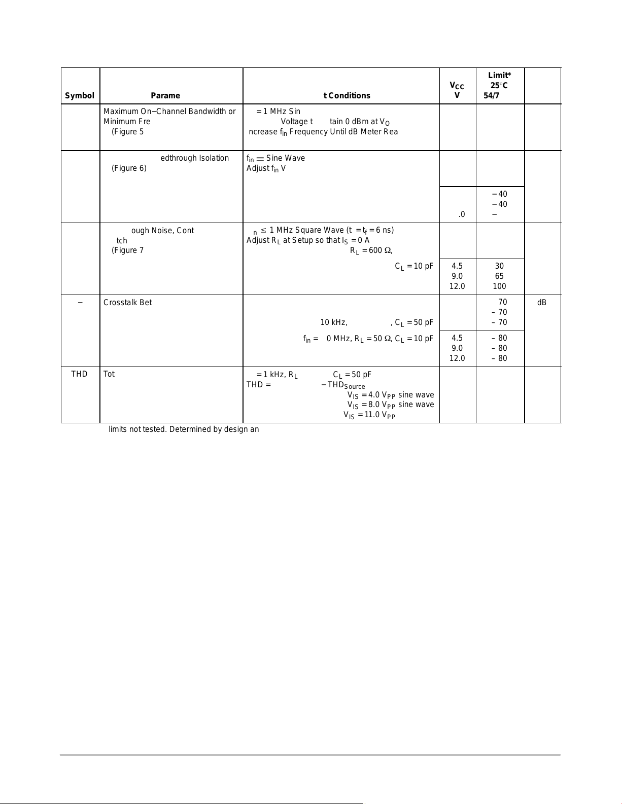
ADDITIONAL APPLICATION CHARACTERISTICS (Voltages Referenced to GND Unless Noted)
ÎÎ
Symbol
BW
ÎÎ
ÎÎ
−
ÎÎ
ÎÎ
ÎÎ
ÎÎ
−
ÎÎ
ÎÎ
ÎÎ
−
ÎÎ
ÎÎ
ÎÎ
ÎÎ
THD
ÎÎ
ÎÎ
ÎÎ
*Guaranteed limits not tested. Determined by design and verified by qualification.
ОООООООО
Parameter
Maximum On−Channel Bandwidth or
Minimum Frequency Response
ОООООООО
(Figure 5)
ОООООООО
Off−Channel Feedthrough Isolation
(Figure 6)
ОООООООО
ОООООООО
ОООООООО
ОООООООО
Feedthrough Noise, Control to
Switch
ОООООООО
(Figure 7)
ОООООООО
ОООООООО
Crosstalk Between Any Two
ОООООООО
Switches
(Figure 12)
ОООООООО
ОООООООО
ОООООООО
Total Harmonic Distortion
(Figure 14)
ОООООООО
ОООООООО
ОООООООО
ОООООООООООО
Test Conditions
fin = 1 MHz Sine Wave
Adjust f
Increase fin Frequency Until dB Meter Reads – 3 dB
Voltage to Obtain 0 dBm at V
ОООООООООООО
in
ОООООООООООО
R
OS
= 50 , CL = 10 pF
L
fin Sine Wave
Adjust f
Voltage to Obtain 0 dBm at V
ОООООООООООО
in
IS
fin = 10 kHz, RL = 600 , CL = 50 pF
ОООООООООООО
ОООООООООООО
fin = 1.0 MHz, RL = 50 , CL = 10 pF
Vin v 1 MHz Square Wave (tr = tf = 6 ns)
Adjust R
ОООООООООООО
at Setup so that IS = 0 A
L
R
= 600 , CL = 50 pF
L
RL = 10 k, CL = 10 pF
ОООООООООООО
fin Sine Wave
ОООООООООООО
Adjust f
Voltage to Obtain 0 dBm at V
in
ОООООООООООО
fin = 10 kHz, RL = 600 , CL = 50 pF
IS
fin = 1.0 MHz, RL = 50 , CL = 10 pF
ОООООООООООО
fin = 1 kHz, RL = 10 k, CL = 50 pF
THD = THD
ОООООООООООО
ОООООООООООО
ОООООООООООО
Measured
− THD
Source
VIS = 4.0 VPP sine wave
V
= 8.0 VPP sine wave
IS
V
= 11.0 VPP sine wave
IS
V
CC
Î
V
4.5
9.0
Î
12.0
Î
4.5
9.0
Î
12.0
4.5
Î
9.0
12.0
Î
4.5
9.0
Î
12.0
4.5
9.0
Î
12.0
4.5
Î
9.0
12.0
Î
4.5
9.0
Î
12.0
Î
4.5
Î
9.0
12.0
Î
Limit*
25°C
ÎÎ
54/74HC
150
160
ÎÎ
160
ÎÎ
− 50
− 50
ÎÎ
− 50
− 40
ÎÎ
− 40
− 40
ÎÎ
60
130
ÎÎ
200
30
65
ÎÎ
100
– 70
ÎÎ
– 70
– 70
ÎÎ
– 80
– 80
ÎÎ
– 80
ÎÎ
0.10
ÎÎ
0.06
0.04
ÎÎ
Î
Unit
MHz
Î
Î
Î
Î
Î
Î
mV
Î
Î
Î
Î
Î
Î
Î
Î
Î
Î
dB
PP
dB
%
http://onsemi.com
5

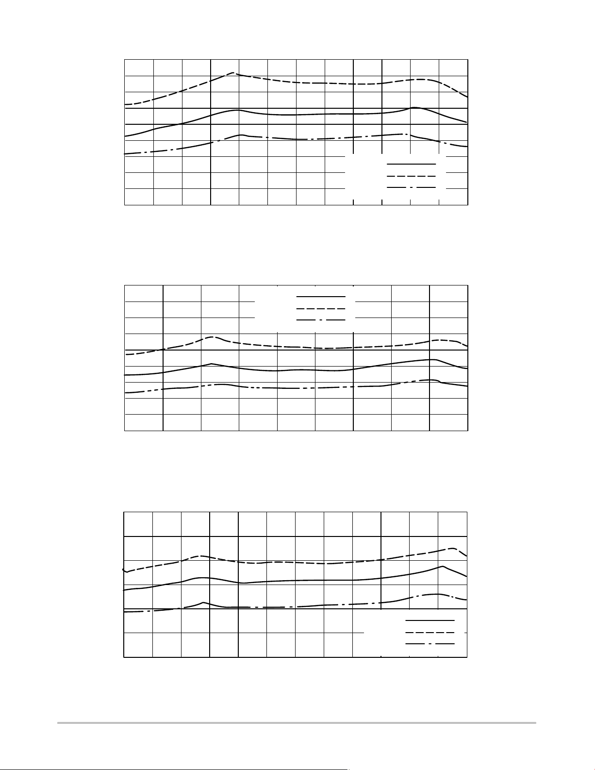
MC74HC4066A
400
350
300
250
200
RON @ 2 V
150
100
50
0
0.00 0.20 0.40 0.60 0.80 1.00 1.20 1.40 1.60 1.80 2.00
Vis, INPUT VOLTAGE (VOLTS), REFERENCED TO GROUND
Figure 1a. Typical On Resistance, VCC = 2.0 V
200
180
160
140
120
100
RON @ 3 V
80
60
40
20
0
0.00 0.20 0.40 0.60 0.80 1.00 1.20 1.40 1.60 1.80 2.00 2.20 2.40 2.60 2.80 3.00
+25 °C
+125°C
−55°C
+25 °C
+125°C
−55°C
Vis, INPUT VOLTAGE (VOLTS), REFERENCED TO GROUND
Figure 1b. Typical On Resistance, V
200
180
160
140
120
100
RON @ 4.5 V
+25 °C
+125°C
−55°C
80
60
40
20
0
0.00 0.50 1.00 1.50 2.00 2.50 3.00 3.50 4.00 4.50
Vis, INPUT VOLTAGE (VOLTS), REFERENCED TO GROUND
Figure 1c. Typical On Resistance, V
CC
= 4.5 V
CC
= 3.0 V
http://onsemi.com
6
MC74HC4066A
90
80
70
60
50
40
RON @ 6 V
30
20
10
0
0.00 0.50 1.00 1.50 2.00 2.50 3.00 3.50 4.00 4.50 5.00 5.50 6.00
Vis, INPUT VOLTAGE (VOLTS), REFERENCED TO GROUND
Figure 1d. Typical On Resistance, VCC = 6.0 V
90
80
70
60
50
40
RON @ 9V
30
20
10
0
0.00 1.00 2.00 3.00 4.00 5.00 6.00 7.00 8.00 9.00
+25 °C
+125°C
−55°C
+25 °C
+125°C
−55°C
Vis, INPUT VOLTAGE (VOLTS), REFERENCED TO GROUND
Figure 1e. Typical On Resistance, V
60
50
40
30
RON @ 12 V
20
10
0
0.00 1.00 2.00 3.00 4.00 5.00 6.00 7.00 8.00 9.00 10.00 11.00 12.00
Vis, INPUT VOLTAGE (VOLTS), REFERENCED TO GROUND
Figure 1f. Typical On Resistance, V
= 9.0 V
CC
= 12.0 V
CC
+25 °C
+125°C
−55°C
http://onsemi.com
7

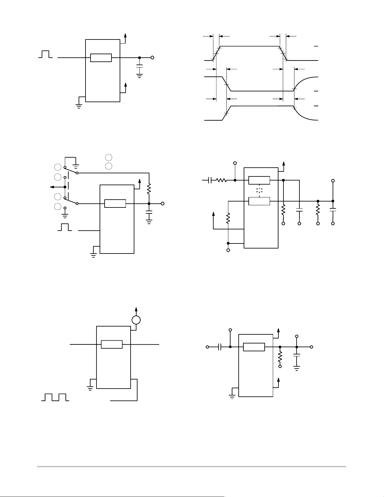
MC74HC4066A
PLOTTER
V
GND
V
PROGRAMMABLE
POWER
MINI COMPUTER
DC ANALYZER
SUPPLY
+−
V
CC
DEVICE
UNDER TEST
ANALOG IN COMMON OUT
GND
Figure 2. On Resistance T est Set−Up
CC
V
CC
14
CC
A
OFF
V
GND
CC
A
ON
V
CC
14
N/C
7
SELECTED
CONTROL
INPUT
V
IL
Figure 3. Maximum Off Channel Leakage Current,
Any One Channel, T est Set−Up
7
SELECTED
CONTROL
INPUT
V
IH
Figure 4. Maximum On Channel Leakage Current,
Test Set−Up
http://onsemi.com
8

MC74HC4066A
V
V
OS
CC
14
f
in
0.1F
7
ON
SELECTED
CONTROL
INPUT
CL*
V
CC
*Includes all probe and jig capacitance.
Figure 5. Maximum On−Channel Bandwidth
Test Set−Up
V
CC/2
V
OS
V
IS
V
CC
14
dB
METER
f
in
0.1F
R
OFF
L
CL*
dB
METER
SELECTED
CONTROL
INPUT
7
*Includes all probe and jig capacitance.
Figure 6. Off−Channel Feedthrough Isolation,
Test Set−Up
V
CC
V
CC/2
14
R
L
OFF/ON
SELECTED
CONTROL
7
INPUT
V
CC
GND
V
≤ 1 MHz
in
t
= tf = 6 ns
r
CONTROL
*Includes all probe and jig capacitance.
Figure 7. Feedthrough Noise, ON/OFF Control to
Analog Out, T est Set−Up
R
L
V
CL*
OS
ANALOG IN
50%
V
CC
I
S
GND
t
PLH
ANALOG OUT
50%
t
PHL
Figure 8. Propagation Delays, Analog In to
Analog Out
http://onsemi.com
9
MC74HC4066A
14
ON
ANALOG OUTANALOG IN
SELECTED
CONTROL
7
INPUT
*Includes all probe and jig capacitance.
Figure 9. Propagation Delay T est Set−Up
POSITIONWHEN TESTING t
1
POSITIONWHEN TESTING t
2
V
CC
1
2
*Includes all probe and jig capacitance.
1
2
14
ON/OFF
SELECTED
CONTROL
INPUT
7
V
CC
TEST
CONTROL
POINT
CL*
V
CC
ANALOG
OUT
50%
10%
90%
t
r
50%
50%
t
t
PZL
PZH
t
t
PLZ
PHZ
t
f
V
CC
GND
HIGH
IMPEDANCE
10%
90%
V
OL
V
OH
HIGH
IMPEDANCE
Figure 10. Propagation Delay, ON/OFF Control
to Analog Out
V
AND t
PHZ
PLZ
V
CC
AND t
1 k
PZL
PZH
f
in
0.1 F
TEST
POINT
CL*
VCC OR GND
*Includes all probe and jig capacitance.
IS
R
L
ON
V
CC
14
V
OS
OFF
R
CL*
R
CL*
L
R
L
SELECTED
CONTROL
INPUT
V
CC/2
L
V
CC/2
7
V
CC/2
Figure 11. Propagation Delay Test Set−Up
V
CC
A
14
N/C
OFF/ON
N/C
SELECTED
CONTROL
7
INPUT
ON/OFF CONTROL
Figure 13. Power Dissipation Capacitance
Test Set−Up
Figure 12. Crosstalk Between Any Two Switches,
Test Set−Up
V
IS
V
CC
V
OS
0.1 F
f
in
7
ON
SELECTED
CONTROL
DISTORTION
CL*
R
L
V
CC/2
V
CC
METER
INPUT
*Includes all probe and jig capacitance.
Figure 14. Total Harmonic Distortion, Test Set−Up
TO
http://onsemi.com
10

dBm
−10
−20
−30
−40
−50
−60
−70
−80
−90
MC74HC4066A
0
FUNDAMENTAL FREQUENCY
DEVICE
SOURCE
1.0 2.0
Figure 15. Plot, Harmonic Distortion
APPLICATION INFORMATION
The ON/OFF Control pins should be at V
levels, V
being recognized as logic high and GND being
CC
or GND logic
CC
recognized as a logic low. Unused analog inputs/outputs
may be left floating (not connected). However, it is
advisable to tie unused analog inputs and outputs to V
CC
or
GND through a low value resistor. This minimizes crosstalk
and feedthrough noise that may be picked−up by the unused
I/O pins.
The maximum analog voltage swings are determined by
the supply voltages V
voltage should not exceed V
and GND. The positive peak analog
CC
. Similarly, the negative peak
CC
analog voltage should not go below GND. In the example
VCC = 12 V
+ 12 V
0 V
ANALOG I/O
ON
14
ANALOG O/I
+ 12 V
0 V
FREQUENCY (kHz)
below, the difference between V
Therefore, using the configuration in Figure 16, a maximum
analog signal of twelve volts peak−to−peak can be
controlled.
When voltage transients above V
are anticipated on the analog channels, external diodes (Dx)
are recommended as shown in Figure 17. These diodes
should be small signal, fast turn−on types able to absorb the
maximum anticipated current surges during clipping. An
alternate method would be to replace the Dx diodes with
Mosorbs (Mosorb™ is an acronym for high current surge
protectors). Mosorbs are fast turn−on devices ideally suited
for precise DC protection with no inherent wear out
mechanism.
3.0
and GND is twelve volts.
CC
and/or below GND
CC
V
CC
D
x
ON
D
x
V
CC
D
16
x
D
x
SELECTED
CONTROL
INPUT
7
OTHER CONTROL
INPUTS
(VCC OR GND)
V
CC
SELECTED
CONTROL
INPUT
7
OTHER CONTROL
INPUTS
(VCC OR GND)
Figure 16. 12 V Application Figure 17. Transient Suppressor Application
http://onsemi.com
11
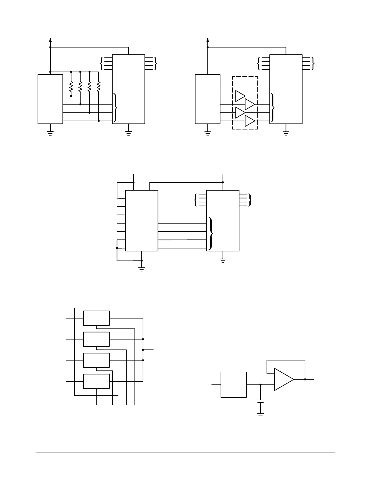
MC74HC4066A
+5 V
LSTTL/
NMOS
ANALOG
SIGNALS
R* R* R* R*
R* = 2 TO 10 k
14
15
5
6
14
HC4066A
CONTROL
INPUTS
7
ANALOG
SIGNALS
+5 V
LSTTL/
NMOS
ANALOG
SIGNALS
HCT
BUFFER
a. Using Pull-Up Resistors b. Using HCT Buffer
Figure 18. LSTTL/NMOS to HCMOS Interface
V
= 5 V VCC = 5 TO 12 V
DD
116 14
13
3
5
7
MC14504
9
11
14
ANALOG
SIGNALS
HC4066A
2
4
6
10
5
6
CONTROL
INPUTS
14
15
78
ANALOG
SIGNALS
14
15
5
6
14
HC4066A
CONTROL
INPUTS
7
ANALOG
SIGNALS
CHANNEL 4
CHANNEL 3
CHANNEL 2
CHANNEL 1
Figure 19. TTL/NMOS−to−CMOS Level Converter
Analog Signal Peak−to−Peak Greater than 5 V
(Also see HC4316A)
1 OF 4
SWITCHES
1 OF 4
SWITCHES
COMMON I/O
1 OF 4
SWITCHES
0.01 F
−
+
EQUIVALENT
LF356 OR
1 OF 4
SWITCHES
1234
CONTROL INPUTS
INPUT
1 OF 4
SWITCHES
Figure 20. 4−Input Multiplexer Figure 21. Sample/Hold Amplifier
OUTPUT
http://onsemi.com
12
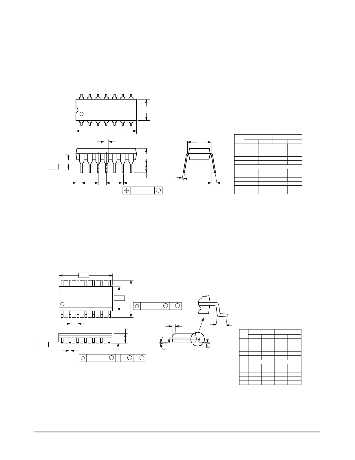
PDIP−14
−T−
SEATING
PLANE
14 8
17
N
HG
MC74HC4066A
PACKAGE DIMENSIONS
N SUFFIX
CASE 646−06
ISSUE N
NOTES:
1. DIMENSIONING AND TOLERANCING
PER ANSI Y14.5M, 1982.
B
A
F
L
C
D
14 PL
0.13 (0.005)
K
J
M
M
2. CONTROLLING DIMENSION: INCH.
3. DIMENSION L TO CENTER OF LEADS
WHEN FORMED PARALLEL.
4. DIMENSION B DOES NOT INCLUDE
MOLD FLASH.
5. ROUNDED CORNERS OPTIONAL.
DIM MIN MAX MIN MAX
A 0.715 0.770 18.16 18.80
B 0.240 0.260 6.10 6.60
C 0.145 0.185 3.69 4.69
D 0.015 0.021 0.38 0.53
F 0.040 0.070 1.02 1.78
G 0.100 BSC 2.54 BSC
H 0.052 0.095 1.32 2.41
J 0.008 0.015 0.20 0.38
K 0.115 0.135 2.92 3.43
L
0.290 0.310 7.37 7.87
M −−− 10 −−− 10
N 0.015 0.039 0.38 1.01
MILLIMETERSINCHES
−T−
SEATING
PLANE
SOIC−14
D SUFFIX
CASE 751A−03
ISSUE G
−A−
14
1
G
D 14 PL
0.25 (0.010) A
8
−B−
P
7 PL
M
0.25 (0.010) B
7
X 45
C
R
K
M
S
B
T
S
M
M
J
NOTES:
1. DIMENSIONING AND TOLERANCING PER
ANSI Y14.5M, 1982.
2. CONTROLLING DIMENSION: MILLIMETER.
3. DIMENSIONS A AND B DO NOT INCLUDE
MOLD PROTRUSION.
4. MAXIMUM MOLD PROTRUSION 0.15 (0.006)
PER SIDE.
5. DIMENSION D DOES NOT INCLUDE
DAMBAR PROTRUSION. ALLOWABLE
DAMBAR PROTRUSION SHALL BE 0.127
(0.005) TOTAL IN EXCESS OF THE D
DIMENSION AT MAXIMUM MATERIAL
F
CONDITION.
DIM MIN MAX MIN MAX
A 8.55 8.75 0.337 0.344
B 3.80 4.00 0.150 0.157
C 1.35 1.75 0.054 0.068
D 0.35 0.49 0.014 0.019
F 0.40 1.25 0.016 0.049
G 1.27 BSC 0.050 BSC
J 0.19 0.25 0.008 0.009
K 0.10 0.25 0.004 0.009
M 0 7 0 7
P 5.80 6.20 0.228 0.244
R 0.25 0.50 0.010 0.019
INCHESMILLIMETERS
http://onsemi.com
13
MC74HC4066A
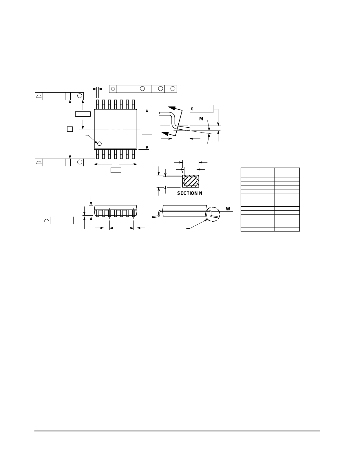
TSSOP−14
PACKAGE DIMENSIONS
DT SUFFIX
CASE 948G−01
ISSUE A
0.10 (0.004)
−T−
SEATING
PLANE
14X REFK
S
U
T
S
N
0.25 (0.010)
U0.15 (0.006) T
S
2X L/2
0.10 (0.004) V
14
M
8
M
L
PIN 1
IDENT.
1
S
U0.15 (0.006) T
A
−V−
B
N
−U−
F
7
DETAIL E
K
K1
J
J1
SECTION N−N
C
D
G
H
DETAIL E
NOTES:
1. DIMENSIONING AND TOLERANCING PER
ANSI Y14.5M, 1982.
2. CONTROLLING DIMENSION: MILLIMETER.
3. DIMENSION A DOES NOT INCLUDE MOLD
FLASH, PROTRUSIONS OR GATE BURRS.
MOLD FLASH OR GATE BURRS SHALL NOT
EXCEED 0.15 (0.006) PER SIDE.
4. DIMENSION B DOES NOT INCLUDE
INTERLEAD FLASH OR PROTRUSION.
INTERLEAD FLASH OR PROTRUSION SHALL
NOT EXCEED 0.25 (0.010) PER SIDE.
5. DIMENSION K DOES NOT INCLUDE
DAMBAR PROTRUSION. ALLOWABLE
DAMBAR PROTRUSION SHALL BE 0.08
(0.003) TOTAL IN EXCESS OF THE K
DIMENSION AT MAXIMUM MATERIAL
CONDITION.
6. TERMINAL NUMBERS ARE SHOWN FOR
REFERENCE ONLY.
7. DIMENSION A AND B ARE TO BE
DETERMINED AT DATUM PLANE −W−.
DIM MIN MAX MIN MAX
A 4.90 5.10 0.193 0.200
B 4.30 4.50 0.169 0.177
C −−− 1.20 −−− 0.047
D 0.05 0.15 0.002 0.006
F 0.50 0.75 0.020 0.030
G 0.65 BSC 0.026 BSC
H 0.50 0.60 0.020 0.024
−W−
J 0.09 0.20 0.004 0.008
J1 0.09 0.16 0.004 0.006
K 0.19 0.30 0.007 0.012
K1 0.19 0.25 0.007 0.010
L 6.40 BSC 0.252 BSC
M 0 8 0 8
INCHESMILLIMETERS
http://onsemi.com
14

SOEIAJ−14
14 8
1
Z
D
e
b
0.13 (0.005)
M
E
7
A
0.10 (0.004)
H
A
1
E
VIEW P
MC74HC4066A
PACKAGE DIMENSIONS
F SUFFIX
CASE 965−01
ISSUE O
L
E
Q
1
M
L
DETAIL P
c
NOTES:
1. DIMENSIONING AND TOLERANCING PER ANSI
Y14.5M, 1982.
2. CONTROLLING DIMENSION: MILLIMETER.
3. DIMENSIONS D AND E DO NOT INCLUDE MOLD
FLASH OR PROTRUSIONS AND ARE MEASURED
AT THE PARTING LINE. MOLD FLASH OR
PROTRUSIONS SHALL NOT EXCEED 0.15 (0.006)
PER SIDE.
4. TERMINAL NUMBERS ARE SHOWN FOR
REFERENCE ONLY.
5. THE LEAD WIDTH DIMENSION (b) DOES NOT
INCLUDE DAMBAR PROTRUSION. ALLOWABLE
DAMBAR PROTRUSION SHALL BE 0.08 (0.003)
TOTAL IN EXCESS OF THE LEAD WIDTH
DIMENSION AT MAXIMUM MATERIAL CONDITION.
DAMBAR CANNOT BE LOCATED ON THE LOWER
RADIUS OR THE FOOT. MINIMUM SPACE
BETWEEN PROTRUSIONS AND ADJACENT LEAD
TO BE 0.46 ( 0.018).
MILLIMETERS
DIM MIN MAX MIN MAX
−−− 2.05 −−− 0.081
A
A
0.05 0.20 0.002 0.008
1
0.35 0.50 0.014 0.020
b
0.18 0.27 0.007 0.011
c
9.90 10.50 0.390 0.413
D
5.10 5.45 0.201 0.215
E
1.27 BSC 0.050 BSC
e
H
7.40 8.20 0.291 0.323
E
0.50 0.85 0.020 0.033
L
L
1.10 1.50 0.043 0.059
E
0
M
Q
0.70 0.90 0.028 0.035
1
−−− 1.42 −−− 0.056
Z
INCHES
10
10
0
http://onsemi.com
15

MC74HC4066A
MOSORB, is a trademark of Semiconductor Components Industries, LLC (SCILLC).
ON Semiconductor and are registered trademarks of Semiconductor Components Industries, LLC (SCILLC). SCILLC reserves the right to make changes without further notice
to any products herein. SCILLC makes no warranty, representation or guarantee regarding the suitability of its products for any particular purpose, nor does SCILLC assume any liability
arising out of the application or use of any product or circuit, and specifically disclaims any and all liability, including without limitation special, consequential or incidental damages.
“Typical” parameters which may be provided in SCILLC data sheets and/or specifications can and do vary in different applications and actual performance may vary over time. All
operating parameters, including “Typicals” must be validated for each customer application by customer’s technical experts. SCILLC does not convey any license under its patent rights
nor the rights of others. SCILLC products are not designed, intended, or authorized for use as components in systems intended for surgical implant into the body, or other applications
intended to support or sustain life, or for any other application in which the failure of the SCILLC product could create a situation where personal injury or death may occur. Should
Buyer purchase or use SCILLC products for any such unintended or unauthorized application, Buyer shall indemnify and hold SCILLC and its officers, employees, subsidiaries, affiliates,
and distributors harmless against all claims, costs, damages, and expenses, and reasonable attorney fees arising out of, directly or indirectly, any claim of personal injury or death
associated with such unintended or unauthorized use, even if such claim alleges that SCILLC was negligent regarding the design or manufacture of the part. SCILLC is an Equal
Opportunity/Affirmative Action Employer. This literature is subject to all applicable copyright laws and is not for resale in any manner.
PUBLICATION ORDERING INFORMATION
LITERATURE FULFILLMENT:
Literature Distribution Center for ON Semiconductor
P.O. Box 61312, Phoenix, Arizona 85082−1312 USA
Phone: 480−829−7710 or 800−344−3860 Toll Free USA/Canada
Fax: 480−829−7709 or 800−344−3867 Toll Free USA/Canada
Email: orderlit@onsemi.com
N. American Technical Support: 800−282−9855 Toll Free
USA/Canada
Japan: ON Semiconductor, Japan Customer Focus Center
2−9−1 Kamimeguro, Meguro−ku, Tokyo, Japan 153−0051
Phone: 81−3−5773−3850
http://onsemi.com
ON Semiconductor Website: http://onsemi.com
Order Literature: http://www.onsemi.com/litorder
For additional information, please contact your
local Sales Representative.
MC74HC4066A/D
16
 Loading...