

MC74AC240, MC74ACT240
Octal Buffer/Line Driver
with 3−State Outputs
The MC74AC240/74ACT240 is an octal buffer and line driver
designed to be employed as a memory address driver, clock driver and
bus oriented transmitter or receiver which provides improved PC
board density.
http://onsemi.com
• 3−State Outputs Drive Bus Lines or Buffer Memory Address
Registers
• Outputs Source/Sink 24 mA
• ′ACT240 Has TTL Compatible Inputs
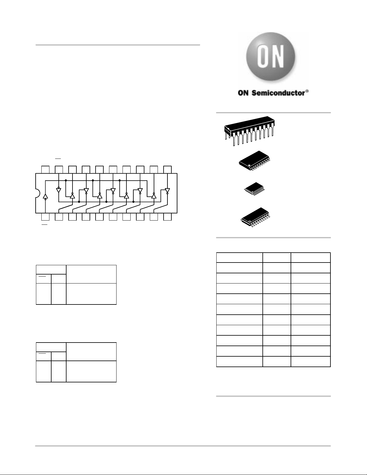
OE
V
CC
2
1920 18 17 16 15 14
21 34567
OE
1
Figure 1. Pinout: 20−Lead Packages Conductors
(Top View)
TRUTH TABLE
Inputs Outputs
OE1D (Pins 12, 14, 16, 18)
L L H
L H L
H X Z
NOTE: H = HIGH Voltage Level
L = LOW Voltage Level
X = Immaterial
Z = High Impedance
TRUTH TABLE
Inputs Outputs
OE2D
L L H
L H L
H X Z
NOTE: H = HIGH Voltage Level
(Pins 3, 5, 7, 9)
L = LOW Voltage Level
X = Immaterial
Z = High Impedance
12
13
8
11
10
9
GND
PDIP−20
N SUFFIX
CASE 738
20
1
20
1
20
1
20
1
SO−20
DW SUFFIX
CASE 751D
TSSOP−20
DT SUFFIX
CASE 948E
EIAJ−20
M SUFFIX
CASE 967
ORDERING INFORMATION
Device Package Shipping
MC74AC240N PDIP−20 18 Units/Rail
MC74ACT240N PDIP−20
MC74AC240DW SOIC−20 38 Units/Rail
MC74AC240DWR2 SOIC−20 1000 Tape & Reel
MC74ACT240DW SOIC−20 38 Units/Rail
MC74ACT240DWR2 SOIC−20
MC74AC240DTR2 TSSOP−20 2500 Tape & Reel
MC74ACT240DTR2 TSSOP−20
MC74AC240MEL EIAJ−20 2000 Tape & Reel
MC74ACT240MEL EIAJ−20
†For information on tape and reel specifications,
including part orientation and tape sizes, please
refer to our Tape and Reel Packaging Specification
Brochure, BRD8011/D.
18 Units/Rail
1000 Tape & Reel
2500 Tape & Reel
2000 Tape & Reel
†
DEVICE MARKING INFORMATION
See general marking information in the device marking
section on page 5 of this data sheet.
Semiconductor Components Industries, LLC, 2004
July, 2004 − Rev. 6
1 Publication Order Number:
MC74AC240/D
MC74AC240, MC74ACT240
r,f
′AC Devices except Schmitt Inputs
In ut Rise and Fall Time (Note 2)
MAXIMUM RATINGS
Symbol Parameter Value Unit
V
CC
V
IN
V
OUT
I
IN
I
OUT
I
CC
T
stg
Maximum ratings are those values beyond which device damage can occur. Maximum ratings applied to the device are individual stress limit
values (not normal operating conditions) and are not valid simultaneously . If these limits are exceeded, device functional operation is not implied,
damage may occur and reliability may be affected.
RECOMMENDED OPERATING CONDITIONS
Symbol Parameter Min Typ Max Unit
V
CC
VIN, V
OUT
tr, t
f
tr, t
f
T
J
T
A
I
OH
I
OL
1. VIN from 30% to 70% VCC; see individual Data Sheets for devices that differ from the typical input rise and fall times.
from 0.8 V to 2.0 V; see individual Data Sheets for devices that differ from the typical input rise and fall times.
2. V
IN
DC Supply Voltage (Referenced to GND) −0.5 to +7.0 V
DC Input Voltage (Referenced to GND) −0.5 to VCC +0.5 V
DC Output Voltage (Referenced to GND) −0.5 to VCC +0.5 V
DC Input Current, per Pin ±20 mA
DC Output Sink/Source Current, per Pin ±50 mA
DC VCC or GND Current per Output Pin ±50 mA
Storage Temperature −65 to +150 °C
Supply Voltage
DC Input Voltage, Output Voltage (Ref. to GND) 0 − V
′AC 2.0 5.0 6.0
′ACT 4.5 5.0 5.5
CC
V
V
VCC @ 3.0 V − 150 −
Input Rise and Fall Time (Note 1)
′
p
p
VCC @ 4.5 V − 40 − ns/V
VCC @ 5.5 V − 25 −
Input Rise and Fall Time (Note 2)
′ACT Devices except Schmitt Inputs
VCC @ 4.5 V − 10 −
VCC @ 5.5 V − 8.0 −
ns/V
Junction Temperature (PDIP) − − 140 °C
Operating Ambient Temperature Range −40 25 85 °C
Output Current − High − − −24 mA
Output Current − Low − − 24 mA
http://onsemi.com
2
MC74AC240, MC74ACT240
y
(V)
ugee
auoee
ugee
V
auoee
V
au u
A
V
V
GND
au
a u Quesce
A
V
V
GND
DC CHARACTERISTICS
74AC 74AC
V
Symbol Parameter
V
IH
Minimum High Level
Input Voltage
CC
3.0 1.5 2.1 2.1 V
4.5 2.25 3.15 3.15 V or VCC − 0.1 V
5.5 2.75 3.85 3.85
V
IL
Maximum Low Level
Input Voltage
3.0 1.5 0.9 0.9 V
4.5 2.25 1.35 1.35 V or VCC − 0.1 V
5.5 2.75 1.65 1.65
V
OH
Minimum High Level
Output Voltage
3.0 2.99 2.9 2.9 I
4.5 4.49 4.4 4.4 V
5.5 5.49 5.4 5.4
3.0 − 2.56 2.46
4.5 − 3.86 3.76
5.5 − 4.86 4.76 −24 mA
V
OL
Maximum Low Level
Output Voltage
3.0 0.002 0.1 0.1 I
4.5 0.001 0.1 0.1 V
5.5 0.001 0.1 0.1
3.0 − 0.36 0.44
4.5 − 0.36 0.44
5.5 − 0.36 0.44 24 mA
I
IN
I
OZ
Maximum Input
Leakage Current
Maximum
3−State
5.5 − ±0.1 ±1.0
5.5 − ±0.5 ±5.0 A VI = VCC, GND
Current
I
OLD
I
OHD
I
CC
†Minimum Dynamic
Output Current
Maximum Quiescent
Supply Current
5.5 − − 75 mA V
5.5 − − −75 mA V
5.5 − 8.0 80
*All outputs loaded; thresholds on input associated with output under test.
†Maximum test duration 2.0 ms, one output loaded at a time.
NOTE: IIN and ICC @ 3.0 V are guaranteed to be less than or equal to the respective limit @ 5.5 V VCC.
TA = +25°C TA =−40°C to +85°C
Typ Guaranteed Limits
Unit Conditions
= 0.1 V
OUT
= 0.1 V
OUT
= −50 A
OUT
*VIN = VIL or V
−12 mA
I
OH
OUT
−24 mA
= 50 A
*VIN = VIL or V
12 mA
I
OL
=
I
V
I
24 mA
,
CC
(OE) = VIL, V
VO = VCC, GND
= 1.65 V Max
OLD
= 3.85 V Min
OHD
=
CC
or
IN
IH
IH
IH
http://onsemi.com
3

MC74AC240, MC74ACT240
O
O
O
O
y
(V)
ugee
V
auoee
V
ugee
V
I
auoee
V
I
au u
A
V
V
GND
au
a u Quesce
A
V
V
GND
AC CHARACTERISTICS (For Figures and Waveforms − See Section 3 of the ON Semiconductor FACT Data Book, DL138/D)
74AC 74AC
Symbol Parameter
t
PLH
t
PHL
t
PZH
t
PZL
t
PHZ
t
PLZ
* Voltage Range 3.3 V is 3.3 V ±0.3 V.
Propagation Delay
Data to Output 5.0 1.5 4.5 6.5 1.0 7.0
Propagation Delay
Data to Output 5.0 1.5 4.5 6.0 1.0 6.5
p
utput Enable Time
p
utput Enable Time
p
utput Disable Time
p
utput Disable Time
VCC*
(V)
3.3 1.5 6.0 8.0 1.0 9.0
3.3 1.5 5.5 8.0 1.0 8.5
3.3 1.5 6.0 10.5 1.0 11.0
5.0 1.5 5.0 7.0 1.0 8.0
3.3 1.5 7.0 10.0 1.0 11.0
5.0 1.5 5.5 8.0 1.0 8.5
3.3 1.5 7.0 10.0 1.0 10.5
5.0 1.5 6.5 9.0 1.0 9.5
3.3 1.5 7.5 10.5 1.0 11.5
5.0 1.5 6.5 9.0 1.0 9.5
Voltage Range 5.0 V is 5.0 V ±0.5 V.
DC CHARACTERISTICS
74ACT 74ACT
V
Symbol Parameter
V
IH
Minimum High Level
Input Voltage
V
IL
Maximum Low Level
Input Voltage
V
OH
Minimum High Level
Output Voltage
CC
4.5 1.5 2.0 2.0
5.5 1.5 2.0 2.0
4.5 1.5 0.8 0.8
5.5 1.5 0.8 0.8
4.5 4.49 4.4 4.4
5.5 5.49 5.4 5.4
4.5 − 3.86 3.76 V
5.5 − 4.86 4.76
V
OL
Maximum Low Level
Output Voltage
4.5 0.001 0.1 0.1
5.5 0.001 0.1 0.1
4.5 − 0.36 0.44 V
5.5 − 0.36 0.44
I
IN
∆I
CCT
I
OZ
Maximum Input
Leakage Current
5.5 − ±0.1 ±1.0
Additional Max. ICC/Input 5.5 0.6 − 1.5 mA VI = VCC − 2.1 V
Maximum
3−State
5.5 − ±0.5 ±5.0 A VI = VCC, GND
Current
I
OLD
I
OHD
I
CC
†Minimum Dynamic
Output Current
Maximum Quiescent
Supply Current
5.5 − − 75 mA V
5.5 − − −75 mA V
5.5 − 8.0 80
*All outputs loaded; thresholds on input associated with output under test.
†Maximum test duration 2.0 ms, one output loaded at a time.
TA = +25°C TA = −40°C to +85°C
Typ Guaranteed Limits
TA = +25°C
C
= 50 pF
L
Min Typ Max Min Max
TA = −40°C
to +85°C
= 50 pF
C
L
Unit
ns 3−5
ns 3−5
ns 3−7
ns 3−8
ns 3−7
ns 3−8
Unit Conditions
V
= 0.1 V
OUT
or VCC − 0.1 V
V
= 0.1 V
OUT
or VCC − 0.1 V
I
= −50 A
OUT
*VIN = VIL or V
OH
I
= 50 A
OUT
*VIN = VIL or V
OL
=
I
CC
V
(OE) = VIL, V
I
VO = VCC, GND
= 1.65 V Max
OLD
= 3.85 V Min
OHD
=
IN
CC
−24 mA
−24 mA
,
or
Fig.
No.
IH
IH
24 mA
24 mA
IH
http://onsemi.com
4

MC74AC240, MC74ACT240
Pro agation Delay
Pro agation Delay
AC CHARACTERISTICS (For Figures and Waveforms − See Section 3 of the ON Semiconductor FACT Data Book, DL138/D)
74ACT 74ACT
TA = −40°C
to +85°C
= 50 pF
C
L
Unit
Symbol Parameter
t
PLH
t
PHL
t
PZH
t
PZL
t
PHZ
t
PLZ
Propagation Delay
Data to Output
Propagation Delay
Data to Output
Output Enable Time 5.0 1.5 7.0 8.5 1.0 9.5 ns 3−7
Output Enable Time 5.0 2.0 7.0 9.5 1.5 10.5 ns 3−8
Output Disable Time 5.0 2.0 8.0 9.5 2.0 10.5 ns 3−7
Output Disable Time 5.0 2.5 6.5 10.0 2.0 10.5 ns 3−8
*Voltage Range 5.0 V is 5.0 V ±0.5 V.
CAPACITANCE
Symbol Parameter
C
IN
C
PD
Input Capacitance 4.5 pF VCC = 5.0 V
Power Dissipation Capacitance 45 pF VCC = 5.0 V
VCC*
(V)
TA = +25°C
C
= 50 pF
L
Min Typ Max Min Max
5.0 1.5 6.0 8.5 1.5 9.5 ns 3−5
5.0 1.5 5.5 7.5 1.5 8.5 ns 3−5
Value
Typ
Unit Test Conditions
Fig.
No.
MARKING DIAGRAMS
PDIP−20 SO−20 TSSOP−20 EIAJ−20
MC74AC240N
AWLYYWW
MC74ACT240N
AWLYYWW
AC240
AWLYYWW
ACT240
AWLYYWW
A = Assembly Location
WL, L = Wafer Lot
YY, Y = Year
WW, W = Work Week
AC
240
ALYW
ACT
240
ALYW
74AC240
AWLYWW
74ACT240
AWLYWW
http://onsemi.com
5

MC74AC240, MC74ACT240
PACKAGE DIMENSIONS
PDIP−20
N SUFFIX
20 PIN PLASTIC DIP PACKAGE
CASE 738−03
ISSUE E
−T−
SEATING
PLANE
H10X
M
B
M
0.25
−A−
NOTES:
1. DIMENSIONING AND TOLERANCING PER ANSI
20
11
B
1
10
C
L
K
M
E
FG
N
20 PL
D
0.25 (0.010) T
J
20 PL
0.25 (0.010) T
M
M
A
M
B
Y14.5M, 1982.
2. CONTROLLING DIMENSION: INCH.
3. DIMENSION L TO CENTER OF LEAD WHEN
FORMED PARALLEL.
4. DIMENSION B DOES NOT INCLUDE MOLD
FLASH.
DIM MIN MAX MIN MAX
A 25.66 27.171.010 1.070
B 6.10 6.600.240 0.260
C 3.81 4.570.150 0.180
D 0.39 0.550.015 0.022
E
F
G 2.54 BSC0.100 BSC
J 0.21 0.380.008 0.015
K 2.80 3.550.110 0.140
L 7.62 BSC0.300 BSC
M
M 0 15 0 15
N 0.51 1.010.020 0.040
MILLIMETERSINCHES
1.27 BSC0.050 BSC
1.27 1.770.050 0.070
SO−20
DW SUFFIX
20 PIN PLASTIC SOIC PACKAGE
CASE 751D−05
ISSUE G
D
20
1
B20X
M
SAS
T
0.25
18X
e
A
11
E
10
h X 45
B
B
A
SEATING
PLANE
A1
T
NOTES:
1. DIMENSIONS ARE IN MILLIMETERS.
2. INTERPRET DIMENSIONS AND TOLERANCES
PER ASME Y14.5M, 1994.
3. DIMENSIONS D AND E DO NOT INCLUDE MOLD
PROTRUSION.
4. MAXIMUM MOLD PROTRUSION 0.15 PER SIDE.
5. DIMENSION B DOES NOT INCLUDE DAMBAR
PROTRUSION. ALLOWABLE PROTRUSION SHALL
BE 0.13 TOTAL IN EXCESS OF B DIMENSION AT
MAXIMUM MATERIAL CONDITION.
MILLIMETERS
DIM MIN MAX
A 2.35 2.65
A1 0.10 0.25
B 0.35 0.49
C 0.23 0.32
D 12.65 12.95
E 7.40 7.60
e 1.27 BSC
H 10.05 10.55
L
C
h 0.25 0.75
L 0.50 0.90
0 7
http://onsemi.com
6

MC74AC240, MC74ACT240
PACKAGE DIMENSIONS
TSSOP−20
DT SUFFIX
20 PIN PLASTIC TSSOP PACKAGE
CASE 948E−02
ISSUE B
20X REFK
S
U0.15 (0.006) T
2X
L/2
0.10 (0.004) V
M
S
U
T
1120
S
B
L
PIN 1
IDENT
110
S
U0.15 (0.006) T
−U−
A
−V−
C
D
G
H
0.100 (0.004)
SEATING
−T−
PLANE
EIAJ−20
M SUFFIX
20 PIN PLASTIC EIAJ PACKAGE
CASE 967−01
ISSUE O
20
110
Z
D
e
b
0.13 (0.005)
M
11
H
E
E
A
0.10 (0.004)
M
VIEW P
A
1
JJ1
N
L
E
N
DETAIL E
K
K1
SECTION N−N
0.25 (0.010)
M
F
DETAIL E
L
DETAIL P
NOTES:
1. DIMENSIONING AND TOLERANCING PER ANSI
Y14.5M, 1982.
2. CONTROLLING DIMENSION: MILLIMETER.
3. DIMENSION A DOES NOT INCLUDE MOLD
FLASH, PROTRUSIONS OR GATE BURRS. MOLD
FLASH OR GATE BURRS SHALL NOT EXCEED
0.15 (0.006) PER SIDE.
4. DIMENSION B DOES NOT INCLUDE
INTERLEAD FLASH OR PROTRUSION.
INTERLEAD FLASH OR PROTRUSION SHALL NOT
EXCEED 0.25 (0.010) PER SIDE.
5. DIMENSION K DOES NOT INCLUDE DAMBAR
PROTRUSION. ALLOWABLE DAMBAR
PROTRUSION SHALL BE 0.08 (0.003) TOTAL IN
EXCESS OF THE K DIMENSION AT MAXIMUM
MATERIAL CONDITION.
6. TERMINAL NUMBERS ARE SHOWN FOR
REFERENCE ONLY.
7. DIMENSION A AND B ARE TO BE
DETERMINED AT DATUM PLANE −W−.
MILLIMETERS
DIMAMIN MAX MIN MAX
B 4.30 4.50 0.169 0.177
C 1.20 0.047
D 0.05 0.15 0.002 0.006
F 0.50 0.75 0.020 0.030
G 0.65 BSC 0.026 BSC
H 0.27 0.37 0.011 0.015
−W−
Q
1
c
J 0.09 0.20 0.004 0.008
J1 0.09 0.16 0.004 0.006
K 0.19 0.30 0.007 0.012
K1 0.19 0.25 0.007 0.010
L 6.40 BSC 0.252 BSC
M 0 8 0 8
NOTES:
1. DIMENSIONING AND TOLERANCING PER ANSI
Y14.5M, 1982.
2. CONTROLLING DIMENSION: MILLIMETER.
3. DIMENSIONS D AND E DO NOT INCLUDE
MOLD FLASH OR PROTRUSIONS AND ARE
MEASURED AT THE PARTING LINE. MOLD FLASH
OR PROTRUSIONS SHALL NOT EXCEED 0.15
(0.006) PER SIDE.
4. TERMINAL NUMBERS ARE SHOWN FOR
REFERENCE ONLY.
5. THE LEAD WIDTH DIMENSION (b) DOES NOT
INCLUDE DAMBAR PROTRUSION. ALLOWABLE
DAMBAR PROTRUSION SHALL BE 0.08 (0.003)
TOTAL IN EXCESS OF THE LEAD WIDTH
DIMENSION AT MAXIMUM MATERIAL CONDITION.
DAMBAR CANNOT BE LOCATED ON THE LOWER
RADIUS OR THE FOOT. MINIMUM SPACE
BETWEEN PROTRUSIONS AND ADJACENT LEAD
TO BE 0.46 ( 0.018).
DIM MIN MAX MIN MAX
A
A
1
b
c
D
E
e
H
E
L
L
E
M
Q
1
Z
6.60 0.260
6.40 0.252
−−− −−−
MILLIMETERS
−−− 2.05 −−− 0.081
0.05 0.20 0.002 0.008
0.35 0.50 0.014 0.020
0.18 0.27 0.007 0.011
12.35 12.80 0.486 0.504
5.10 5.45 0.201 0.215
1.27 BSC 0.050 BSC
7.40 8.20 0.291 0.323
0.50 0.85 0.020 0.033
1.10 1.50 0.043 0.059
10
0
0.70 0.90 0.028 0.035
−−− 0.81 −−− 0.032
INCHES
INCHES
0
10
http://onsemi.com
7

MC74AC240, MC74ACT240
ON Semiconductor and are registered trademarks of Semiconductor Components Industries, LLC (SCILLC). SCILLC reserves the right to make changes without further notice
to any products herein. SCILLC makes no warranty, representation or guarantee regarding the suitability of its products for any particular purpose, nor does SCILLC assume any liability
arising out of the application or use of any product or circuit, and specifically disclaims any and all liability, including without limitation special, consequential or incidental damages.
“Typical” parameters which may be provided in SCILLC data sheets and/or specifications can and do vary in different applications and actual performance may vary over time. All
operating parameters, including “Typicals” must be validated for each customer application by customer’s technical experts. SCILLC does not convey any license under its patent rights
nor the rights of others. SCILLC products are not designed, intended, or authorized for use as components in systems intended for surgical implant into the body, or other applications
intended to support or sustain life, or for any other application in which the failure of the SCILLC product could create a situation where personal injury or death may occur. Should
Buyer purchase or use SCILLC products for any such unintended or unauthorized application, Buyer shall indemnify and hold SCILLC and its officers, employees, subsidiaries, affiliates,
and distributors harmless against all claims, costs, damages, and expenses, and reasonable attorney fees arising out of, directly or indirectly, any claim of personal injury or death
associated with such unintended or unauthorized use, even if such claim alleges that SCILLC was negligent regarding the design or manufacture of the part. SCILLC is an Equal
Opportunity/Affirmative Action Employer. This literature is subject to all applicable copyright laws and is not for resale in any manner.
PUBLICATION ORDERING INFORMATION
LITERATURE FULFILLMENT:
Literature Distribution Center for ON Semiconductor
P.O. Box 61312, Phoenix, Arizona 85082−1312 USA
Phone: 480−829−7710 or 800−344−3860 Toll Free USA/Canada
Fax: 480−829−7709 or 800−344−3867 Toll Free USA/Canada
Email: orderlit@onsemi.com
N. American Technical Support: 800−282−9855 Toll Free
USA/Canada
Japan: ON Semiconductor, Japan Customer Focus Center
2−9−1 Kamimeguro, Meguro−ku, Tokyo, Japan 153−0051
Phone: 81−3−5773−3850
http://onsemi.com
ON Semiconductor Website: http://onsemi.com
Order Literature: http://www.onsemi.com/litorder
For additional information, please contact your
local Sales Representative.
MC74AC240/D
8

WWW.ALLDATASHEET.COM
Copyright © Each Manufacturing Company.
All Datasheets cannot be modified without permission.
This datasheet has been download from :
www.AllDataSheet.com
100% Free DataSheet Search Site.
Free Download.
No Register.
Fast Search System.
www.AllDataSheet.com
 Loading...