

查询AC138ALYW供应商
MC74AC138, MC74ACT138
1−of−8
Decoder/Demultiplexer
The MC74AC138/74ACT138 is a high−speed 1−of−8
decoder/demultiplexer. This device is ideally suited for high−speed
bipolar memory chip select address decoding.
The multiple input enables allow parallel expansion to a 1−of−24
decoder using just three MC74AC138/74ACT138 devices or a
1−of−32 decoder using four MC74AC138/74ACT138 devices and one
inverter.
• Demultiplexing Capability
• Multiple Input Enable for Easy Expansion
• Active LOW Mutually Exclusive Outputs
• Outputs Source/Sink 24 mA
• ′ACT138 Has TTL Compatible Inputs
w These devices are available in Pb−free package(s). Specifications herein
apply to both standard and Pb−free devices. Please see our website at
www.onsemi.com for specific Pb−free orderable part numbers, or
contact your local ON Semiconductor sales office or representative.
V
O0O1O2O3O4O5O
CC
1516 14 13 12 11 10
6
9
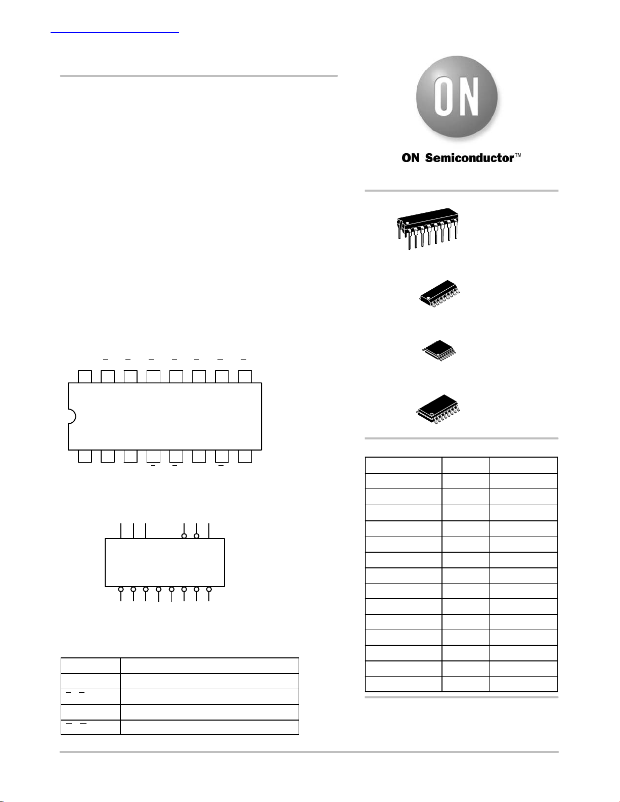
16
http://onsemi.com
1
16
1
16
1
DIP−16
N SUFFIX
CASE 648
SO−16
D SUFFIX
CASE 751B
TSSOP−16
DT SUFFIX
CASE 948F
21 34567
3
8
O
GNDA0A1A2E1E2E
7
Figure 1. Pinout: 16−Lead Packages Conductors
(Top View)
A0A1A
2
O1O2O3O4O5O6O
O
0
E1E2E
3
7
Figure 2. Logic Symbol
PIN ASSIGNMENT
PIN FUNCTION
A0−A
E1−E
E
3
O0−O
2
2
7
Address Inputs
Enable Inputs
Enable Input
Outputs
EIAJ−16
16
1
M SUFFIX
CASE 966
ORDERING INFORMATION
Device Package Shipping
MC74AC138N
MC74ACT138N
MC74AC138D
MC74ACT138D
MC74AC138DR2 2500 Tape & Reel
MC74ACT138DR2 2500 Tape & Reel
MC74AC138DT
MC74ACT138DT
MC74AC138DTR2
MC74ACT138DTR2
MC74AC138M
MC74ACT138M
MC74AC138MEL
MC74ACT138MEL
PDIP−16
PDIP−16
SOIC−16
SOIC−16
SOIC−16
SOIC−16
TSSOP−16
TSSOP−16
TSSOP−16
TSSOP−16
EIAJ−16
EIAJ−16
EIAJ−16
EIAJ−16
25 Units/Rail
25 Units/Rail
48 Units/Rail
48 Units/Rail
96 Units/Rail
96 Units/Rail
2500 Tape & Reel
2500 Tape & Reel
50 Units/Rail
50 Units/Rail
2000 Tape & Reel
2000 Tape & Reel
DEVICE MARKING INFORMATION
See general marking information in the device marking
section on page 6 of this data sheet.
© Semiconductor Components Industries, LLC, 2006
March, 2006 − Rev. 6
1 Publication Order Number:
MC74AC138/D
MC74AC138, MC74ACT138
FUNCTIONAL DESCRIPTION
The MC74AC138/74ACT138 high−speed 1−of−8
decoder/demultiplexer accepts three binary weighted inputs
(A
, A1, A2) and, when enabled, provides eight mutually
0
exclusive active−LOW outputs (O
0−O7
). The
MC74AC138/74ACT138 features three Enable inputs, two
active−LOW (E
outputs will be HIGH unless E
, E2) and one active−HIGH (E3). All
1
and E2 are LOW and E3 is
1
TRUTH TABLE
Inputs Outputs
E1E
H X X X X X H H H H H H H H
X H X X X X H H H H H H H H
X X L X X X H H H H H H H H
L L H L L L L H H H H H H H
L L H H L L H L H H H H H H
L L H L H L H H L H H H H H
L L H H H L H H H L H H H H
L L H L L H H H H H L H H H
L L H H L H H H H H H L H H
L L H L H H H H H H H H L H
L L H H H H H H H H H H H L
H = HIGH Voltage Level
L = LOW Voltage Level
X = Immaterial
E
A
A
2
3
0
A2O0O1O2O3O
1
HIGH. This multiple enabled function allows easy parallel
expansion of the device to a 1−of−32 (5 lines to 32 lines)
decoder with just four MC74AC138/74ACT138 devices
and one inverter (See Figure 4). The
MC74AC138/74ACT138 can be used as an 8−output
demultiplexer by using one of the active LOW Enable inputs
as the data input and the other Enable inputs as strobes. The
Enable inputs which are not used must be permanently tied
to their appropriate active−HIGH or active−LOW state.
O5O6O
4
7
E
E1E
3
A2A
0
7
NOTE: This diagram is provided only for the understanding of logic
operations and should not be used to estimate propagation
delays.
A
1
0
0
0
6
0
5
4
2
0
0
3
0
2
0
1
0
Figure 3. Logic Diagram
http://onsemi.com
2
MC74AC138, MC74ACT138
A
0
A
1
A
2
′04
A
3
A
4
A0A1A
2
H
123 123 123 123
E
A0A1A
2
E
A0A1A
2
E
A0A1A
2
E
0
001020304050607
0
0
0
001020304050607
0
001020304050607
0
001020304050607
0
31
Figure 4. Expansion to 1−of−32 Decoding
MAXIMUM RATINGS*
Symbol Parameter Value Unit
V
V
V
I
IN
I
OUT
I
CC
T
CC
IN
OUT
stg
DC Supply Voltage (Referenced to GND) −0.5 to +7.0 V
DC Input Voltage (Referenced to GND) −0.5 to VCC +0.5 V
DC Output Voltage (Referenced to GND) −0.5 to VCC +0.5 V
DC Input Current, per Pin ±20 mA
DC Output Sink/Source Current, per Pin ±50 mA
DC VCC or GND Current per Output Pin ±50 mA
Storage Temperature −65 to +150 °C
*Maximum Ratings are those values beyond which damage to the device may occur. Functional operation should be restricted to the Recom-
mended Operating Conditions.
RECOMMENDED OPERATING CONDITIONS
Symbol Parameter Min Typ Max Unit
V
CC
VIN, V
tr, t
f
tr, t
f
T
J
T
A
I
OH
I
OL
Supply Voltage
DC Input Voltage, Output Voltage (Ref. to GND) 0 − V
OUT
Input Rise and Fall Time (Note 1)
′AC Devices except Schmitt Inputs
Input Rise and Fall Time (Note 2)
′ACT Devices except Schmitt Inputs
Junction Temperature (PDIP) − − 140 °C
Operating Ambient Temperature Range −40 25 85 °C
Output Current − High − − −24 mA
Output Current − Low − − 24 mA
1. VIN from 30% to 70% VCC; see individual Data Sheets for devices that differ from the typical input rise and fall times.
from 0.8 V to 2.0 V; see individual Data Sheets for devices that differ from the typical input rise and fall times.
2. V
IN
′AC 2.0 5.0 6.0
′ACT 4.5 5.0 5.5
CC
V
V
VCC @ 3.0 V − 150 −
VCC @ 4.5 V − 40 − ns/V
VCC @ 5.5 V − 25 −
VCC @ 4.5 V − 10 −
VCC @ 5.5 V − 8.0 −
ns/V
http://onsemi.com
3
MC74AC138, MC74ACT138
DC CHARACTERISTICS
V
CC
Symbol Parameter
V
IH
Minimum High Level
Input Voltage
(V)
3.0 1.5 2.1 2.1 V
4.5 2.25 3.15 3.15 V or VCC − 0.1 V
5.5 2.75 3.85 3.85
V
IL
Maximum Low Level
Input Voltage
3.0 1.5 0.9 0.9 V
4.5 2.25 1.35 1.35 V or VCC − 0.1 V
5.5 2.75 1.65 1.65
V
OH
Minimum High Level
Output Voltage
3.0 2.99 2.9 2.9 I
4.5 4.49 4.4 4.4 V
5.5 5.49 5.4 5.4
3.0 − 2.56 2.46 −12 mA
4.5 − 3.86 3.76 I
5.5 − 4.86 4.76 −24 mA
V
OL
Maximum Low Level
Output Voltage
3.0 0.002 0.1 0.1 I
4.5 0.001 0.1 0.1 V
5.5 0.001 0.1 0.1
3.0 − 0.36 0.44 12 mA
4.5 − 0.36 0.44 I
5.5 − 0.36 0.44 24 mA
I
IN
I
OLD
I
OHD
I
CC
Maximum Input
Leakage Current
†Minimum Dynamic
Output Current
Maximum Quiescent
Supply Current
5.5 − ±0.1 ±1.0 μA VI = VCC, GND
5.5 − − 75 mA V
5.5 − − −75 mA V
5.5 − 8.0 80 μA VIN = VCC or GND
*All outputs loaded; thresholds on input associated with output under test.
†Maximum test duration 2.0 ms, one output loaded at a time.
NOTE: I
and ICC @ 3.0 V are guaranteed to be less than or equal to the respective limit @ 5.5 V VCC.
IN
TA = +25°C
Typ Guaranteed Limits
74AC 74AC
TA =
−40°C to
+85°C
Unit Conditions
= 0.1 V
OUT
= 0.1 V
OUT
= −50 μA
OUT
*VIN = VIL or V
V
OH
OUT
−24 mA
= 50 μA
*VIN = VIL or V
V
OL
OLD
OHD
24 mA
= 1.65 V Max
= 3.85 V Min
IH
IH
http://onsemi.com
4

MC74AC138, MC74ACT138
AC CHARACTERISTICS (For Figures and Waveforms − See Section 3 of the ON Semiconductor FACT Data Book, DL138/D)
74AC 74AC
TA = −40°C
to +85°C
= 50 pF
C
L
Unit
ns 3−6
ns 3−6
ns 3−6
ns 3−6
ns 3−6
ns 3−6
Symbol
t
PLH
t
PHL
t
PLH
t
PHL
t
PLH
t
PHL
Propagation Delay
A
to O
n
n
Propagation Delay
A
to O
n
n
Propagation Delay
E
or E2 to O
1
n
Propagation Delay
E
or E2 to O
1
n
Propagation Delay
E
to O
3
n
Propagation Delay
E
to O
3
n
*Voltage Range 3.3 V is 3.3 V ±0.3 V.
*Voltage Range 5.0 V is 5.0 V ±0.5 V.
Parameter
VCC*
(V)
TA = +25°C
C
= 50 pF
L
Min Typ Max Min Max
3.3 1.5 8.5 13.0 1.5 15.0
5.0 1.5 6.5 9.5 1.5 10.5
3.3 1.5 8.0 12.5 1.5 14.0
5.0 1.5 6.0 9.0 1.5 10.5
3.3 1.5 11.0 15.0 1.5 16.0
5.0 1.5 8.0 11.0 1.5 12.0
3.3 1.5 9.5 13.5 1.5 15.0
5.0 1.5 7.0 9.5 1.5 10.5
3.3 1.5 11.0 15.5 1.5 16.5
5.0 1.5 8.0 11.0 1.5 12.5
3.3 1.5 8.5 13.0 1.5 14.0
5.0 1.5 6.0 8.0 1.0 9.5
Fig.
No.
DC CHARACTERISTICS
V
CC
Symbol Parameter
V
IH
Minimum High Level
Input Voltage
V
IL
Maximum Low Level
Input Voltage
V
OH
Minimum High Level
Output Voltage
(V)
4.5 1.5 2.0 2.0
5.5 1.5 2.0 2.0 or VCC − 0.1 V
4.5 1.5 0.8 0.8
5.5 1.5 0.8 0.8 or VCC − 0.1 V
4.5 4.49 4.4 4.4
5.5 5.49 5.4 5.4
4.5 − 3.86 3.76 V
5.5 − 4.86 4.76 −24 mA
V
OL
Maximum Low Level
Output Voltage
4.5 0.001 0.1 0.1
5.5 0.001 0.1 0.1
4.5 − 0.36 0.44 V
5.5 − 0.36 0.44 24 mA
I
IN
ΔI
I
OLD
I
OHD
I
CC
CCT
Maximum Input
Leakage Current
5.5 − ±0.1 ±1.0 μA VI = VCC, GND
Additional Max. ICC/Input 5.5 0.6 − 1.5 mA VI = VCC − 2.1 V
†Minimum Dynamic
Output Current
Maximum Quiescent
Supply Current
5.5 − − 75 mA V
5.5 − − −75 mA V
5.5 − 8.0 80 μA VIN = VCC or GND
*All outputs loaded; thresholds on input associated with output under test.
†Maximum test duration 2.0 ms, one output loaded at a time.
TA = +25°C
Typ Guaranteed Limits
74ACT 74ACT
TA =
−40°C to
+85°C
Unit Conditions
V
= 0.1 V
V
I
OUT
OUT
OUT
= 0.1 V
= −50 μA
V
V
V
*VIN = VIL or V
OH
OUT
−24 mA
= 50 μA
I
V
I
*VIN = VIL or V
I
OL
OLD
OHD
24 mA
= 1.65 V Max
= 3.85 V Min
IH
IH
http://onsemi.com
5

MC74AC138, MC74ACT138
AC CHARACTERISTICS (For Figures and Waveforms − See Section 3 of the ON Semiconductor FACT Data Book, DL138/D)
74ACT 74ACT
TA = −40°C
to +85°C
= 50 pF
C
L
Unit
Symbol
t
PLH
t
PHL
t
PLH
t
PHL
t
PLH
t
PHL
Propagation Delay
A
to O
n
n
Propagation Delay
A
to O
n
n
Propagation Delay
E
or E2 to O
1
Propagation Delay
E
or E2 to O
1
Propagation Delay
E
O
3 to
n
Propagation Delay
E
to O
3
n
Parameter
n
n
*Voltage Range 5.0 V is 5.0 V ± 0.5 V
CAPACITANCE
Symbol Parameter
C
IN
C
PD
Input Capacitance 4.5 pF VCC = 5.0 V
Power Dissipation Capacitance 60 pF VCC = 5.0 V
VCC*
(V)
TA = +25°C
C
= 50 pF
L
Min Typ Max Min Max
5.0 1.5 7.0 10.5 1.5 11.5 ns 3−6
5.0 1.5 6.5 10.5 1.5 11.5 ns 3−6
5.0 2.5 8.0 11.5 2.0 12.5 ns 3−6
5.0 2.0 7.5 11.5 2.0 12.5 ns 3−6
5.0 2.5 8.0 12.0 2.0 13.0 ns 3−6
5.0 2.0 6.5 10.5 1.5 11.5 ns 3−6
Value
Typ
Unit Test Conditions
Fig.
No.
MARKING DIAGRAMS
DIP−16 SO−16 TSSOP−16 EIAJ−16
MC74AC138N
AWLYYWW
MC74ACT138N
AWLYYWW
AC138
AWLYWW
ACT138
AWLYWW
A = Assembly Location
WL, L = Wafer Lot
YY, Y = Year
WW, W = Work Week
AC
138
ALYW
ACT
138
ALYW
74AC138
ALYW
74ACT138
ALYW
http://onsemi.com
6

−A−
916
B
18
F
S
H
G
D
16 PL
0.25 (0.010) T
−A−
16 9
18
G
−T−
SEATING
PLANE
D
16 PL
0.25 (0.010) A
M
T
MC74AC138, MC74ACT138
PACKAGE DIMENSIONS
PDIP−16
N SUFFIX
16 PIN PLASTIC DIP PACKAGE
CASE 648−08
ISSUE R
C
SEATING
−T−
PLANE
K
M
A
J
M
16 PIN PLASTIC SOIC PACKAGE
CASE 751B−05
−B−
K
S
B
8 PLP
0.25 (0.010) B
C
S
L
SO−16
D SUFFIX
ISSUE J
M
R
M
S
X 45
NOTES:
1. DIMENSIONING AND TOLERANCING PER ANSI
Y14.5M, 1982.
2. CONTROLLING DIMENSION: INCH.
3. DIMENSION L TO CENTER OF LEADS WHEN
FORMED PARALLEL.
4. DIMENSION B DOES NOT INCLUDE MOLD FLASH.
5. ROUNDED CORNERS OPTIONAL.
DIM MIN MAX MIN MAX
A 0.740 0.770 18.80 19.55
B 0.250 0.270 6.35 6.85
C 0.145 0.175 3.69 4.44
D 0.015 0.021 0.39 0.53
F 0.040 0.70 1.02 1.77
G 0.100 BSC 2.54 BSC
M
_
J
H 0.050 BSC 1.27 BSC
J 0.008 0.015 0.21 0.38
K 0.110 0.130 2.80 3.30
L 0.295 0.305 7.50 7.74
M 0 10 0 10
S 0.020 0.040 0.51 1.01
NOTES:
1. DIMENSIONING AND TOLERANCING PER ANSI
Y14.5M, 1982.
2. CONTROLLING DIMENSION: MILLIMETER.
3. DIMENSIONS A AND B DO NOT INCLUDE
MOLD PROTRUSION.
4. MAXIMUM MOLD PROTRUSION 0.15 (0.006)
PER SIDE.
5. DIMENSION D DOES NOT INCLUDE DAMBAR
PROTRUSION. ALLOWABLE DAMBAR
PROTRUSION SHALL BE 0.127 (0.005) TOTAL
IN EXCESS OF THE D DIMENSION AT
MAXIMUM MATERIAL CONDITION.
DIM MIN MAX MIN MAX
F
A 9.80 10.00 0.386 0.393
B 3.80 4.00 0.150 0.157
C 1.35 1.75 0.054 0.068
D 0.35 0.49 0.014 0.019
F 0.40 1.25 0.016 0.049
G 1.27 BSC 0.050 BSC
J 0.19 0.25 0.008 0.009
K 0.10 0.25 0.004 0.009
M 0 7 0 7
P 5.80 6.20 0.229 0.244
R 0.25 0.50 0.010 0.019
MILLIMETERSINCHES
____
INCHESMILLIMETERS
____
http://onsemi.com
7

0.10 (0.004)
−T−
SEATING
PLANE
L
U0.15 (0.006) T
PIN 1
IDENT.
U0.15 (0.006) T
D
S
2X L/2
S
MC74AC138, MC74ACT138
PACKAGE DIMENSIONS
TSSOP−16
DT SUFFIX
16 PIN PLASTIC TSSOP PACKAGE
CASE948F−01
ISSUE O
16X REFK
T
U
B
−U−
S
N
H
S
J1
J
N
DETAIL E
DETAIL E
0.25 (0.010)
F
K
K1
SECTION N−N
M
NOTES:
1. DIMENSIONING AND TOLERANCING PER ANSI
Y14.5M, 1982.
2. CONTROLLING DIMENSION: MILLIMETER.
3. DIMENSION A DOES NOT INCLUDE MOLD FLASH.
PROTRUSIONS OR GATE BURRS. MOLD FLASH
OR GATE BURRS SHALL NOT EXCEED 0.15
(0.006) PER SIDE.
4. DIMENSION B DOES NOT INCLUDE INTERLEAD
FLASH OR PROTRUSION. INTERLEAD FLASH OR
PROTRUSION SHALL NOT EXCEED
0.25 (0.010) PER SIDE.
5. DIMENSION K DOES NOT INCLUDE DAMBAR
PROTRUSION. ALLOWABLE DAMBAR
PROTRUSION SHALL BE 0.08 (0.003) TOTAL IN
EXCESS OF THE K DIMENSION AT MAXIMUM
MATERIAL CONDITION.
6. TERMINAL NUMBERS ARE SHOWN FOR
REFERENCE ONLY.
7. DIMENSION A AND B ARE TO BE DETERMINED
AT DATUM PLANE −W−.
DIM MIN MAX MIN MAX
A 4.90 5.10 0.193 0.200
B 4.30 4.50 0.169 0.177
C −−− 1.20 −−− 0.047
D 0.05 0.15 0.002 0.006
F 0.50 0.75 0.020 0.030
G 0.65 BSC 0.026 BSC
H 0.18 0.28 0.007 0.011
J 0.09 0.20 0.004 0.008
−W−
J1 0.09 0.16 0.004 0.006
K 0.19 0.30 0.007 0.012
K1 0.19 0.25 0.007 0.010
L 6.40 BSC 0.252 BSC
M 0 8 0 8
____
INCHESMILLIMETERS
0.10 (0.004) V
16
1
M
9
8
A
−V−
C
G
16 9
1
Z
D
e
b
0.13 (0.005)
M
8
H
E
E
A
A
1
0.10 (0.004)
EIAJ−16
M SUFFIX
16 PIN PLASTIC EIAJ PACKAGE
CASE966−01
ISSUE O
L
E
Q
M
_
L
DETAIL P
VIEW P
NOTES:
1. DIMENSIONING AND TOLERANCING PER ANSI
Y14.5M, 1982.
2. CONTROLLING DIMENSION: MILLIMETER.
3. DIMENSIONS D AND E DO NOT INCLUDE MOLD
FLASH OR PROTRUSIONS AND ARE MEASURED
1
c
AT THE PARTING LINE. MOLD FLASH OR
PROTRUSIONS SHALL NOT EXCEED 0.15 (0.006)
PER SIDE.
4. TERMINAL NUMBERS ARE SHOWN FOR
REFERENCE ONLY.
5. THE LEAD WIDTH DIMENSION (b) DOES NOT
INCLUDE DAMBAR PROTRUSION. ALLOWABLE
DAMBAR PROTRUSION SHALL BE 0.08 (0.003)
TOTAL IN EXCESS OF THE LEAD WIDTH
DIMENSION AT MAXIMUM MATERIAL CONDITION.
DAMBAR CANNOT BE LOCATED ON THE LOWER
RADIUS OR THE FOOT. MINIMUM SPACE
BETWEEN PROTRUSIONS AND ADJACENT LEAD
TO BE 0.46 ( 0.018).
MILLIMETERS
DIM MIN MAX MIN MAX
−−− 2.05 −−− 0.081
A
A
0.05 0.20 0.002 0.008
1
0.35 0.50 0.014 0.020
b
0.18 0.27 0.007 0.011
c
9.90 10.50 0.390 0.413
D
5.10 5.45 0.201 0.215
E
1.27 BSC 0.050 BSC
e
H
7.40 8.20 0.291 0.323
E
0.50 0.85 0.020 0.033
L
L
1.10 1.50 0.043 0.059
E
0
M
_
Q
0.70 0.90 0.028 0.035
1
−−− 0.78 −−− 0.031
Z
INCHES
10
_
10
0
_
_
http://onsemi.com
8

Notes
MC74AC138, MC74ACT138
http://onsemi.com
9

Notes
MC74AC138, MC74ACT138
http://onsemi.com
10

Notes
MC74AC138, MC74ACT138
ON Semiconductor and are registered trademarks of Semiconductor Components Industries, LLC (SCILLC). SCILLC reserves the right to make changes without further notice
to any products herein. SCILLC makes no warranty, representation or guarantee regarding the suitability of its products for any particular purpose, nor does SCILLC assume any liability
arising out of the application or use of any product or circuit, and specifically disclaims any and all liability, including without limitation special, consequential or incidental damages.
“Typical” parameters which may be provided in SCILLC data sheets and/or specifications can and do vary in different applications and actual performance may vary over time. All
operating parameters, including “Typicals” must be validated for each customer application by customer’s technical experts. SCILLC does not convey any license under its patent rights
nor the rights of others. SCILLC products are not designed, intended, or authorized for use as components in systems intended for surgical implant into the body, or other applications
intended to support or sustain life, or for any other application in which the failure of the SCILLC product could create a situation where personal injury or death may occur. Should
Buyer purchase or use SCILLC products for any such unintended or unauthorized application, Buyer shall indemnify and hold SCILLC and its officers, employees, subsidiaries, affiliates,
and distributors harmless against all claims, costs, damages, and expenses, and reasonable attorney fees arising out of, directly or indirectly, any claim of personal injury or death
associated with such unintended or unauthorized use, even if such claim alleges that SCILLC was negligent regarding the design or manufacture of the part. SCILLC is an Equal
Opportunity/Affirmative Action Employer. This literature is subject to all applicable copyright laws and is not for resale in any manner.
PUBLICATION ORDERING INFORMATION
LITERATURE FULFILLMENT:
Literature Distribution Center for ON Semiconductor
P.O. Box 61312, Phoenix, Arizona 85082−1312 USA
Phone: 480−829−7710 or 800−344−3860 Toll Free USA/Canada
Fax: 480−829−7709 or 800−344−3867 Toll Free USA/Canada
Email: orderlit@onsemi.com
N. American Technical Support: 800−282−9855 Toll Free
USA/Canada
Japan: ON Semiconductor, Japan Customer Focus Center
2−9−1 Kamimeguro, Meguro−ku, Tokyo, Japan 153−0051
Phone: 81−3−5773−3850
http://onsemi.com
ON Semiconductor Website: http://onsemi.com
Order Literature: http://www.onsemi.com/litorder
For additional information, please contact your
local Sales Representative.
MC74AC138/D
11
 Loading...