

Page 1
MC74AC74, MC74ACT74
Dual D−Type Positive
Edge−Triggered Flip−Flop
The MC74AC74/74ACT74 is a dual D−type flip−flop with
Asynchronous Clear and Set inputs and complementary (Q,Q)
outputs. Information at the input is transferred to the outputs on the
positive edge of the clock pulse. Clock triggering occurs at a voltage
level of the clock pulse and is not directly related to the transition time
of the positive-going pulse. After the Clock Pulse input threshold
voltage has been passed, the Data input is locked out and information
present will not be transferred to the outputs until the next rising edge
of the Clock Pulse input.
Asynchronous Inputs:
LOW input to SD (Set) sets Q to HIGH level
LOW input to CD (Clear) sets Q to LOW level
Clear and Set are independent of clock
Simultaneous LOW on CD and SD makes both Q and Q HIGH
Features
• Outputs Source/Sink 24 mA
• ′ACT74 Has TTL Compatible Inputs
• Pb−Free Packages are Available
V
CD2D2CP2SD2Q2Q
CC
1314 12 11 10 9 8
C
D1
Q
D
1
1
CP
Q
S
1
1
D1
CP
2
D
2
S
D2
Q
Q
C
D2
2
2
2
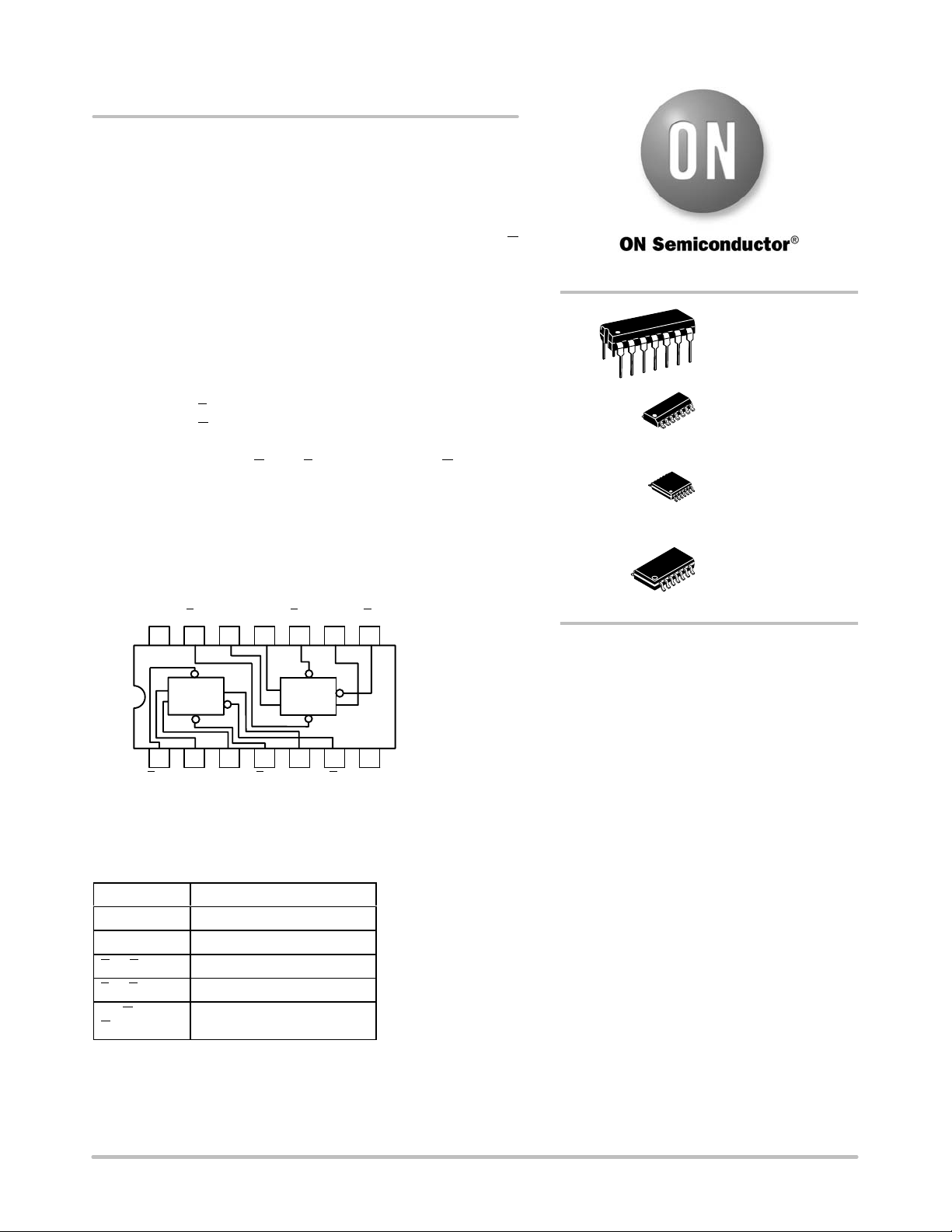
http://onsemi.com
PDIP−14
N SUFFIX
14
1
14
1
CASE 646
SOIC−14
D SUFFIX
CASE 751A
TSSOP−14
14
1
DT SUFFIX
CASE 948G
SOEIAJ−14
14
1
M SUFFIX
CASE 965
ORDERING INFORMATION
See detailed ordering and shipping information in the package
dimensions section on page 7 of this data sheet.
21 34567
C
D1D1
CP1SD1Q1Q
GND
1
Figure 1. Pinout: 14−Lead Packages Conductors
(Top View)
PIN ASSIGNMENT
PIN FUNCTION
D1, D
2
CP1, CP
CD1, C
SD1, S
2
D2
D2
Q1, Q1, Q2,
Q
2
© Semiconductor Components Industries, LLC, 2006
October, 2006 − Rev. 7
Data Inputs
Clock Pulse Inputs
Direct Clear Inputs
Direct Set Inputs
Outputs
1 Publication Order Number:
MC74AC74/D
Page 2
TRUTH TABLE (Each Half)
Inputs Outputs
S
D
L H X X H L
H L X X L H
L L X X H H
H H H H L
H H L L H
H H L X Q
NOTE: H = HIGH Voltage Level
C
D
CP D Q Q
0
L = LOW Voltage Level
X = Immaterial;
= LOW-to-HIGH Clock Transition
Q0(Q0) = Previous Q(Q) before LOW-to-HIGH
Transition of Clock
S
D
MC74AC74, MC74ACT74
Q
0
Q
S
D1
D
S
D2
D2CP
1
1
Q
2
CP
Q
1
C
D1
1
Q
2
CD
2
2
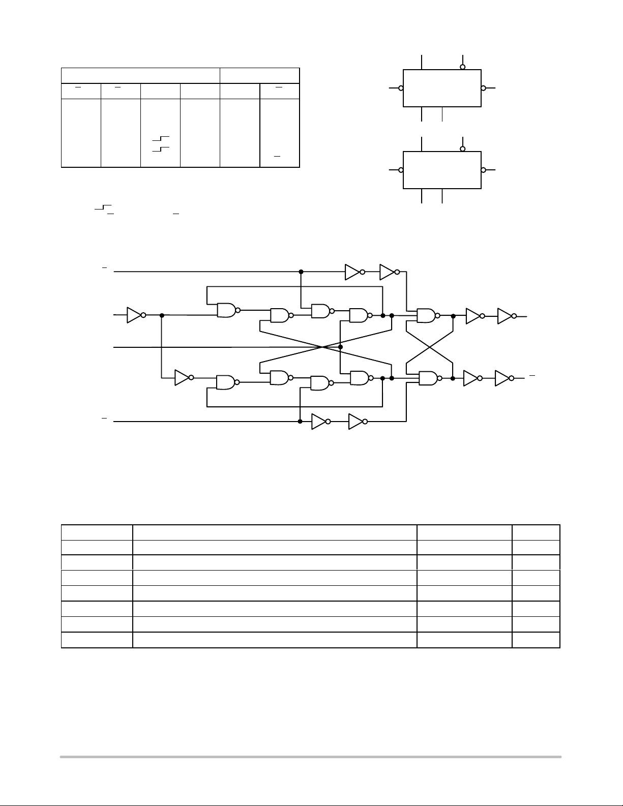
Figure 2. Logic Symbol
D
Q
CP
Q
C
D
NOTE: This diagram is provided only for the understanding of
logic operations and should not be used to estimate
propagation delays.
Figure 3. Logic Diagram
MAXIMUM RATINGS
Symbol Parameter Value Unit
V
CC
V
in
V
out
I
in
I
out
I
CC
T
stg
Stresses exceeding Maximum Ratings may damage the device. Maximum Ratings are stress ratings only. Functional operation above the
Recommended Operating Conditions is not implied. Extended exposure to stresses above the Recommended Operating Conditions may affect
device reliability.
DC Supply Voltage (Referenced to GND) −0.5 to +7.0 V
DC Input Voltage (Referenced to GND) −0.5 to VCC +0.5 V
DC Output Voltage (Referenced to GND) −0.5 to VCC +0.5 V
DC Input Current, per Pin ±20 mA
DC Output Sink/Source Current, per Pin ±50 mA
DC VCC or GND Current per Output Pin ±50 mA
Storage Temperature −65 to +150 °C
http://onsemi.com
2
Page 3
MC74AC74, MC74ACT74
RECOMMENDED OPERATING CONDITIONS
Symbol Parameter Min Typ Max Unit
V
CC
Vin, V
tr, t
f
tr, t
f
T
J
T
A
I
OH
I
OL
out
Supply Voltage
DC Input Voltage, Output Voltage (Ref. to GND) 0 − V
Input Rise and Fall Time (Note )
′AC Devices except Schmitt Inputs
Input Rise and Fall Time (Note )
′ACT Devices except Schmitt Inputs
Junction Temperature (PDIP) − − 140 °C
Operating Ambient Temperature Range −40 25 85 °C
Output Current − High − − −24 mA
Output Current − Low − − 24 mA
1. Vin from 30% to 70% VCC; see individual Data Sheets for devices that differ from the typical input rise and fall times.
2. Vin from 0.8 V to 2.0 V; see individual Data Sheets for devices that differ from the typical input rise and fall times.
DC CHARACTERISTICS
V
Symbol Parameter
V
IH
Minimum High Level
Input Voltage
V
IL
Maximum Low Level
Input Voltage
V
OH
Minimum High Level
Output Voltage
V
OL
Maximum Low Level
Output Voltage
I
IN
Maximum Input
Leakage Current
I
OLD
I
OHD
I
CC
†Minimum Dynamic
Output Current
Maximum Quiescent
Supply Current
*All outputs loaded; thresholds on input associated with output under test.
†Maximum test duration 2.0 ms, one output loaded at a time.
NOTE: IIN and ICC @ 3.0 V are guaranteed to be less than or equal to the respective limit @ 5.5 V VCC.
CC
(V)
3.0 1.5 2.1 2.1 V
4.5 2.25 3.15 3.15 V or VCC − 0.1 V
5.5 2.75 3.85 3.85
3.0 1.5 0.9 0.9 V
4.5 2.25 1.35 1.35 V or VCC − 0.1 V
5.5 2.75 1.65 1.65
3.0 2.99 2.9 2.9
4.5 4.49 4.4 4.4 V
5.5 5.49 5.4 5.4
3.0 − 2.56 2.46 −12 mA
4.5 − 3.86 3.76 I
5.5 − 4.86 4.76 −24 mA
3.0 0.002 0.1 0.1
4.5 0.001 0.1 0.1 V
5.5 0.001 0.1 0.1
3.0 − 0.36 0.44 12 mA
4.5 − 0.36 0.44 I
5.5 − 0.36 0.44 24 mA
5.5 − ±0.1 ±1.0
5.5 − − 75 mA V
5.5 − − −75 mA V
5.5 − 4.0 40
′AC 2.0 5.0 6.0
′ACT 4.5 5.0 5.5
CC
VCC @ 3.0 V − 150 −
VCC @ 4.5 V − 40 − ns/V
VCC @ 5.5 V − 25 −
VCC @ 4.5 V − 10 −
VCC @ 5.5 V − 8.0 −
74AC 74AC
TA =
TA = +25°C
−40°C to
Unit Conditions
+85°C
Typ Guaranteed Limits
= 0.1 V
OUT
= 0.1 V
OUT
I
= −50 mA
OUT
*VIN = VIL or V
V
OH
I
OUT
−24 mA
= 50 mA
*VIN = VIL or V
mA
mA
V
OL
VI = VCC, GND
OLD
OHD
VIN = VCC or GND
24 mA
= 1.65 V Max
= 3.85 V Min
V
V
ns/V
IH
IH
http://onsemi.com
3
Page 4
MC74AC74, MC74ACT74
AC CHARACTERISTICS (For Figures and Waveforms − See Section 3 of the ON Semiconductor FACT Data Book, DL138/D)
74AC 74AC
TA = −40°C
to +85°C
CL = 50 pF
TA = −40°C
to +85°C
CL = 50 pF
Unit
MHz 3−3
ns 3−6
ns 3−6
ns 3−6
ns 3−6
Unit
ns 3−9
ns 3−9
ns 3−6
ns 3−9
Symbol Parameter
f
t
t
t
t
max
PLH
PHL
PLH
PHL
Maximum Clock
Frequency
Propagation Delay
CDn or SDn to Qn or Q
Propagation Delay
CDn or S
to Qn or Q
Dn
Propagation Delay
CPn to Qn or Q
n
Propagation Delay
CPn to Qn or Q
n
n
n
*Voltage Range 3.3 V is 3.3 V ±0.3 V.
Voltage Range 5.0 V is 5.0 V ±0.5 V.
AC OPERATING REQUIREMENTS
Symbol Parameter
t
s
t
h
t
w
t
rec
*Voltage Range 3.3 V is 3.3 V ±0.3 V.
Voltage Range 5.0 V is 5.0 V ±0.5 V.
Set-up Time, HIGH or LOW 3.3 1.5 4.0 4.5
Dn to CP
n
Hold Time, HIGH or LOW 3.3 −2.0 0.5 0.5
Dn to CP
CPn or CDn or S
n
Dn
Pulse Width 5.0 2.5 4.5 5.0
Recovery TIme 3.3 −2.5 0 0
CDn or SDn to CP 5.0 −2.0 0 0
VCC*
(V)
TA = +25°C
CL = 50 pF
Min Typ Max Min Max
3.3 100 125 − 95 −
5.0 140 160 − 125 −
3.3 5.0 8.0 12.5 4.0 13.0
5.0 3.5 6.0 9.0 3.0 10.0
3.3 4.0 10.5 12.0 3.5 13.5
5.0 3.0 8.0 9.5 2.5 10.5
3.3 4.5 8.0 13.5 4.0 16.0
5.0 3.5 6.0 10.0 3.0 10.5
3.3 3.5 8.0 14.0 3.5 14.5
5.0 2.5 6.0 10.0 2.5 10.5
74AC 74AC
VCC*
(V)
TA = +25°C
CL = 50 pF
Typ Guaranteed Minimum
5.0 1.0 3.0 3.0
5.0 −1.5 0.5 0.5
3.3 3.0 5.5 7.0
Fig.
No.
Fig.
No.
http://onsemi.com
4
Page 5

MC74AC74, MC74ACT74
DC CHARACTERISTICS
V
CC
Symbol Parameter
V
IH
Minimum High Level
Input Voltage
V
IL
Maximum Low Level
Input Voltage
V
OH
Minimum High Level
Output Voltage
V
OL
Maximum Low Level
Output Voltage
I
IN
Maximum Input
Leakage Current
DI
I
OLD
I
OHD
I
CC
CCT
Additional Max. ICC/Input 5.5 0.6 − 1.5 mA VI = VCC − 2.1 V
†Minimum Dynamic
Output Current
Maximum Quiescent
Supply Current
*All outputs loaded; thresholds on input associated with output under test.
†Maximum test duration 2.0 ms, one output loaded at a time.
TA = +25°C
(V)
Typ Guaranteed Limits
4.5 1.5 2.0 2.0
5.5 1.5 2.0 2.0 or VCC − 0.1 V
4.5 1.5 0.8 0.8
5.5 1.5 0.8 0.8 or VCC − 0.1 V
4.5 4.49 4.4 4.4
5.5 5.49 5.4 5.4
4.5 − 3.86 3.76 V
5.5 − 4.86 4.76 −24 mA
4.5 0.001 0.1 0.1
5.5 0.001 0.1 0.1
4.5 − 0.36 0.44 V
5.5 − 0.36 0.44 24 mA
5.5 − ±0.1 ±1.0
5.5 − − 75 mA V
5.5 − − −75 mA V
5.5 − 4.0 40
74ACT 74ACT
TA =
−40°C to
+85°C
Unit Conditions
V
= 0.1 V
V
I
OUT
OUT
OUT
= 0.1 V
= −50 mA
V
V
V
*VIN = VIL or V
I
OH
I
V
OUT
−24 mA
= 50 mA
*VIN = VIL or V
24 mA
= 1.65 V Max
= 3.85 V Min
mA
mA
I
OL
VI = VCC, GND
OLD
OHD
VIN = VCC or GND
IH
IH
AC CHARACTERISTICS (For Figures and Waveforms − See Section 3 of the ON Semiconductor FACT Data Book, DL138/D)
74ACT 74ACT
TA = −40°C
to +85°C
CL = 50 pF
Unit
Symbol Parameter
f
t
t
t
t
max
PLH
PHL
PLH
PHL
Maximum Clock
Frequency
Propagation Delay
CDn or SDn to Qn or Q
Propagation Delay
CDn or S
to Qn or Q
Dn
Propagation Delay
CPn to Qn or Q
n
Propagation Delay
CPn to Qn or Q
n
n
n
*Voltage Range 5.0 V is 5.0 V ±0.5 V.
VCC*
(V)
TA = +25°C
CL = 50 pF
Min Typ Max Min Max
5.0 145 210 − 125 − MHz 3−3
5.0 3.0 5.5 9.5 2.5 10.5 ns 3−6
5.0 3.0 6.0 10.0 3.0 11.5 ns 3−6
5.0 4.0 7.5 11.0 4.0 13.0 ns 3−6
5.0 3.5 6.0 10.0 3.0 11.5 ns 3−6
Fig.
No.
http://onsemi.com
5
Page 6

AC OPERATING REQUIREMENTS
Symbol Parameter
t
s
t
h
t
w
t
rec
Set-up Time, HIGH or LOW
Dn to CP
n
Hold Time, HIGH or LOW
Dn to CP
CPn or CDn or S
n
Dn
Pulse Width
Recovery TIme
CDn or SDn to CP
*Voltage Range 5.0 V is 5.0 V ±0.5 V.
CAPACITANCE
Symbol Parameter
C
IN
C
PD
Input Capacitance 4.5 pF VCC = 5.0 V
Power Dissipation Capacitance 35 pF VCC = 5.0 V
MC74AC74, MC74ACT74
74ACT 74ACT
VCC*
(V)
5.0 1.0 3.0 3.5 ns 3−9
5.0 −0.5 1.0 1.0 ns 3−9
5.0 3.0 5.0 6.0 ns 3−6
5.0 −2.5 0 0 ns 3−9
TA = +25°C
CL = 50 pF
Typ Guaranteed Minimum
Value
Typ
TA = −40°C
to +85°C
Unit
CL = 50 pF
Unit Test Conditions
Fig.
No.
http://onsemi.com
6
Page 7

ORDERING INFORMATION
MC74AC74, MC74ACT74
Device Package Shipping
MC74AC74N PDIP−14
MC74AC74NG PDIP−14
MC74ACT74N PDIP−14
MC74ACT74NG PDIP−14
MC74AC74D SOIC−14
MC74AC74DG SOIC−14
MC74AC74DR2 SOIC−14
MC74AC74DR2G SOIC−14
MC74ACT74D SOIC−14
MC74ACT74DG SOIC−14
MC74ACT74DR2 SOIC−14
MC74ACT74DR2G SOIC−14
MC74AC74DT TSSOP−14* 96 Units/Rail
MC74AC74DTR2 TSSOP−14*
MC74AC74DTR2G TSSOP−14*
MC74ACT74DT TSSOP−14* 96 Units/Rail
MC74ACT74DTR2 TSSOP−14*
MC74ACT74DTR2G TSSOP−14*
MC74AC74MEL SOEIAJ−14
MC74AC74MELG SOEIAJ−14
MC74ACT74MEL SOEIAJ−14
MC74ACT74MELG
†For information on tape and reel specifications, including part orientation and tape sizes, please refer to our Tape and Reel Packaging
Specifications Brochure, BRD8011/D.
*This package is inherently Pb−Free.
(Pb−Free)
25 Units/Rail
(Pb−Free)
55 Units/Rail
(Pb−Free)
2500/Tape & Reel
(Pb−Free)
55 Units/Rail
(Pb−Free)
2500/Tape & Reel
(Pb−Free)
2500/Tape & Reel
2500/Tape & Reel
(Pb−Free)
2000/Tape & Reel
SOEIAJ−14
(Pb−Free)
†
http://onsemi.com
7
Page 8

MC74AC74, MC74ACT74
MARKING DIAGRAMS
PDIP−14 SOIC−14 TSSOP−14
MC74AC74N
AWLYYWWG
MC74ACT74N
AWLYYWWG
14
AC74G
AWLYWW
1
14
ACT74G
AWLYWW
1
A = Assembly Location
WL, L = Wafer Lot
YY, Y = Year
WW, W = Work Week
G or G = Pb−Free Package
(Note: Microdot may be in either location)
ALYWG
ACT
ALYWG
AC
74
74
SOEIAJ−14
74AC74
ALYWG
G
74ACT74
ALYWG
G
http://onsemi.com
8
Page 9

−T−
SEATING
PLANE
14 8
17
N
HG
MC74AC74, MC74ACT74
PACKAGE DIMENSIONS
PDIP−14
CASE 646−06
ISSUE P
NOTES:
1. DIMENSIONING AND TOLERANCING PER ANSI
Y14.5M, 1982.
2. CONTROLLING DIMENSION: INCH.
B
A
F
L
C
D
14 PL
0.13 (0.005)
K
J
M
M
3. DIMENSION L TO CENTER OF LEADS WHEN
FORMED PARALLEL.
4. DIMENSION B DOES NOT INCLUDE MOLD FLASH.
5. ROUNDED CORNERS OPTIONAL.
DIM MIN MAX MIN MAX
A 0.715 0.770 18.16 19.56
B 0.240 0.260 6.10 6.60
C 0.145 0.185 3.69 4.69
D 0.015 0.021 0.38 0.53
F 0.040 0.070 1.02 1.78
G 0.100 BSC 2.54 BSC
H 0.052 0.095 1.32 2.41
J 0.008 0.015 0.20 0.38
K 0.115 0.135 2.92 3.43
L
0.290 0.310 7.37 7.87
M −−− 10 −−− 10
N 0.015 0.039 0.38 1.01
MILLIMETERSINCHES
__
http://onsemi.com
9
Page 10

−T−
SEATING
PLANE
MC74AC74, MC74ACT74
SOIC−14
CASE 751A−03
ISSUE H
NOTES:
1. DIMENSIONING AND TOLERANCING PER
−A−
14
1
8
−B−
7
P 7 PL
0.25 (0.010) B
M
M
G
F
J
D 14 PL
0.25 (0.010) A
M
T
R X 45
C
K
S
B
S
_
M
SOLDERING FOOTPRINT*
7X
7.04
1
14X
0.58
14X
1.52
ANSI Y14.5M, 1982.
2. CONTROLLING DIMENSION: MILLIMETER.
3. DIMENSIONS A AND B DO NOT INCLUDE
MOLD PROTRUSION.
4. MAXIMUM MOLD PROTRUSION 0.15 (0.006)
PER SIDE.
5. DIMENSION D DOES NOT INCLUDE
DAMBAR PROTRUSION. ALLOWABLE
DAMBAR PROTRUSION SHALL BE 0.127
(0.005) TOTAL IN EXCESS OF THE D
DIMENSION AT MAXIMUM MATERIAL
CONDITION.
DIM MIN MAX MIN MAX
A 8.55 8.75 0.337 0.344
B 3.80 4.00 0.150 0.157
C 1.35 1.75 0.054 0.068
D 0.35 0.49 0.014 0.019
F 0.40 1.25 0.016 0.049
G 1.27 BSC 0.050 BSC
J 0.19 0.25 0.008 0.009
K 0.10 0.25 0.004 0.009
M 0 7 0 7
__ __
P 5.80 6.20 0.228 0.244
R 0.25 0.50 0.010 0.019
INCHESMILLIMETERS
1.27
PITCH
DIMENSIONS: MILLIMETERS
*For additional information on our Pb−Free strategy and soldering
details, please download the ON Semiconductor Soldering and
Mounting Techniques Reference Manual, SOLDERRM/D.
http://onsemi.com
10
Page 11

MC74AC74, MC74ACT74
PACKAGE DIMENSIONS
TSSOP−14
CASE 948G−01
ISSUE B
0.10 (0.004)
−T−
SEATING
PLANE
14X REFK
S
U
T
S
N
0.25 (0.010)
U0.15 (0.006) T
S
2X L/2
0.10 (0.004) V
14
M
8
M
L
PIN 1
IDENT.
1
S
U0.15 (0.006) T
A
−V−
B
N
−U−
F
7
DETAIL E
K
K1
J
J1
SECTION N−N
C
D
G
H
DETAIL E
NOTES:
1. DIMENSIONING AND TOLERANCING PER
ANSI Y14.5M, 1982.
2. CONTROLLING DIMENSION: MILLIMETER.
3. DIMENSION A DOES NOT INCLUDE MOLD
FLASH, PROTRUSIONS OR GATE BURRS.
MOLD FLASH OR GATE BURRS SHALL NOT
EXCEED 0.15 (0.006) PER SIDE.
4. DIMENSION B DOES NOT INCLUDE
INTERLEAD FLASH OR PROTRUSION.
INTERLEAD FLASH OR PROTRUSION SHALL
NOT EXCEED 0.25 (0.010) PER SIDE.
5. DIMENSION K DOES NOT INCLUDE DAMBAR
PROTRUSION. ALLOWABLE DAMBAR
PROTRUSION SHALL BE 0.08 (0.003) TOTAL
IN EXCESS OF THE K DIMENSION AT
MAXIMUM MATERIAL CONDITION.
6. TERMINAL NUMBERS ARE SHOWN FOR
REFERENCE ONLY.
7. DIMENSION A AND B ARE TO BE
DETERMINED AT DATUM PLANE −W−.
INCHESMILLIMETERS
−W−
DIM MIN MAX MIN MAX
A 4.90 5.10 0.193 0.200
B 4.30 4.50 0.169 0.177
C −−− 1.20 −−− 0.047
D 0.05 0.15 0.002 0.006
F 0.50 0.75 0.020 0.030
G 0.65 BSC 0.026 BSC
H 0.50 0.60 0.020 0.024
J 0.09 0.20 0.004 0.008
J1 0.09 0.16 0.004 0.006
K 0.19 0.30 0.007 0.012
K1 0.19 0.25 0.007 0.010
L 6.40 BSC 0.252 BSC
M 0 8 0 8
____
SOLDERING FOOTPRINT*
7.06
1
14X
0.36
14X
1.26
DIMENSIONS: MILLIMETERS
*For additional information on our Pb−Free strategy and soldering
details, please download the ON Semiconductor Soldering and
Mounting Techniques Reference Manual, SOLDERRM/D.
http://onsemi.com
11
0.65
PITCH
Page 12

14 8
1
Z
D
e
b
0.13 (0.005)
M
E
7
A
0.10 (0.004)
H
A
1
MC74AC74, MC74ACT74
SOEIAJ−14
CASE 965−01
ISSUE A
L
E
E
VIEW P
_
M
L
DETAIL P
NOTES:
1. DIMENSIONING AND TOLERANCING PER ANSI
Y14.5M, 1982.
2. CONTROLLING DIMENSION: MILLIMETER.
3. DIMENSIONS D AND E DO NOT INCLUDE MOLD
FLASH OR PROTRUSIONS AND ARE MEASURED
AT THE PARTING LINE. MOLD FLASH OR
Q
1
c
PROTRUSIONS SHALL NOT EXCEED 0.15 (0.006)
PER SIDE.
4. TERMINAL NUMBERS ARE SHOWN FOR
REFERENCE ONLY.
5. THE LEAD WIDTH DIMENSION (b) DOES NOT
INCLUDE DAMBAR PROTRUSION. ALLOWABLE
DAMBAR PROTRUSION SHALL BE 0.08 (0.003)
TOTAL IN EXCESS OF THE LEAD WIDTH
DIMENSION AT MAXIMUM MATERIAL CONDITION.
DAMBAR CANNOT BE LOCATED ON THE LOWER
RADIUS OR THE FOOT. MINIMUM SPACE
BETWEEN PROTRUSIONS AND ADJACENT LEAD
TO BE 0.46 ( 0.018).
MILLIMETERS
DIM MIN MAX MIN MAX
−−− 2.05 −−− 0.081
A
A
0.05 0.20 0.002 0.008
1
0.35 0.50 0.014 0.020
b
0.10 0.20 0.004 0.008
c
9.90 10.50 0.390 0.413
D
5.10 5.45 0.201 0.215
E
1.27 BSC 0.050 BSC
e
H
7.40 8.20 0.291 0.323
E
0.50 0.85 0.020 0.033
0.50
L
1.10 1.50 0.043 0.059
E
0
M
_
Q
0.70 0.90 0.028 0.035
1
−−− 1.42 −−− 0.056
Z
INCHES
10
_
10
0
_
_
ON Semiconductor and are registered trademarks of Semiconductor Components Industries, LLC (SCILLC). SCILLC reserves the right to make changes without further notice
to any products herein. SCILLC makes no warranty, representation or guarantee regarding the suitability of its products for any particular purpose, nor does SCILLC assume any liability
arising out of the application or use of any product or circuit, and specifically disclaims any and all liability, including without limitation special, consequential or incidental damages.
“Typical” parameters which may be provided in SCILLC data sheets and/or specifications can and do vary in different applications and actual performance may vary over time. All
operating parameters, including “Typicals” must be validated for each customer application by customer’s technical experts. SCILLC does not convey any license under its patent rights
nor the rights of others. SCILLC products are not designed, intended, or authorized for use as components in systems intended for surgical implant into the body, or other applications
intended to support or sustain life, or for any other application in which the failure of the SCILLC product could create a situation where personal injury or death may occur. Should
Buyer purchase or use SCILLC products for any such unintended or unauthorized application, Buyer shall indemnify and hold SCILLC and its officers, employees, subsidiaries, affiliates,
and distributors harmless against all claims, costs, damages, and expenses, and reasonable attorney fees arising out of, directly or indirectly, any claim of personal injury or death
associated with such unintended or unauthorized use, even if such claim alleges that SCILLC was negligent regarding the design or manufacture of the part. SCILLC is an Equal
Opportunity/Affirmative Action Employer. This literature is subject to all applicable copyright laws and is not for resale in any manner.
PUBLICATION ORDERING INFORMATION
LITERATURE FULFILLMENT:
Literature Distribution Center for ON Semiconductor
P.O. Box 5163, Denver, Colorado 80217 USA
Phone: 303−675−2175 or 800−344−3860 Toll Free USA/Canada
Fax: 303−675−2176 or 800−344−3867 Toll Free USA/Canada
Email: orderlit@onsemi.com
N. American Technical Support: 800−282−9855 Toll Free
USA/Canada
Europe, Middle East and Africa Technical Support:
Phone: 421 33 790 2910
Japan Customer Focus Center
Phone: 81−3−5773−3850
http://onsemi.com
ON Semiconductor Website: www.onsemi.com
Order Literature: http://www.onsemi.com/orderlit
For additional information, please contact your local
Sales Representative
MC74AC74/D
12
 Loading...