

Page 1
MC74AC573, MC74ACT573
Octal Buffer/Line Driver
with 3−State Outputs
The MC74AC573/74ACT573 is a high−speed octal latch with
buffered common Latch Enable (LE) and buffered common Output
Enable (OE
The MC74AC573/74ACT573 is functionally identical to the
MC74AC373/74ACT373 but has inputs and outputs on opposite sides.
) inputs.
http://onsemi.com
Features
• Inputs and Outputs on Opposite Sides of Package Allowing Easy
Interface with Microprocessors
• Useful as Input or Output Port for Microprocessors
• Functionally Identical to MC74AC373/74ACT373
• 3−State Outputs for Bus Interfacing
• Outputs Source/Sink 24 mA
• ′ACT573 Has TTL Compatible Inputs
• Pb−Free Packages are Available*
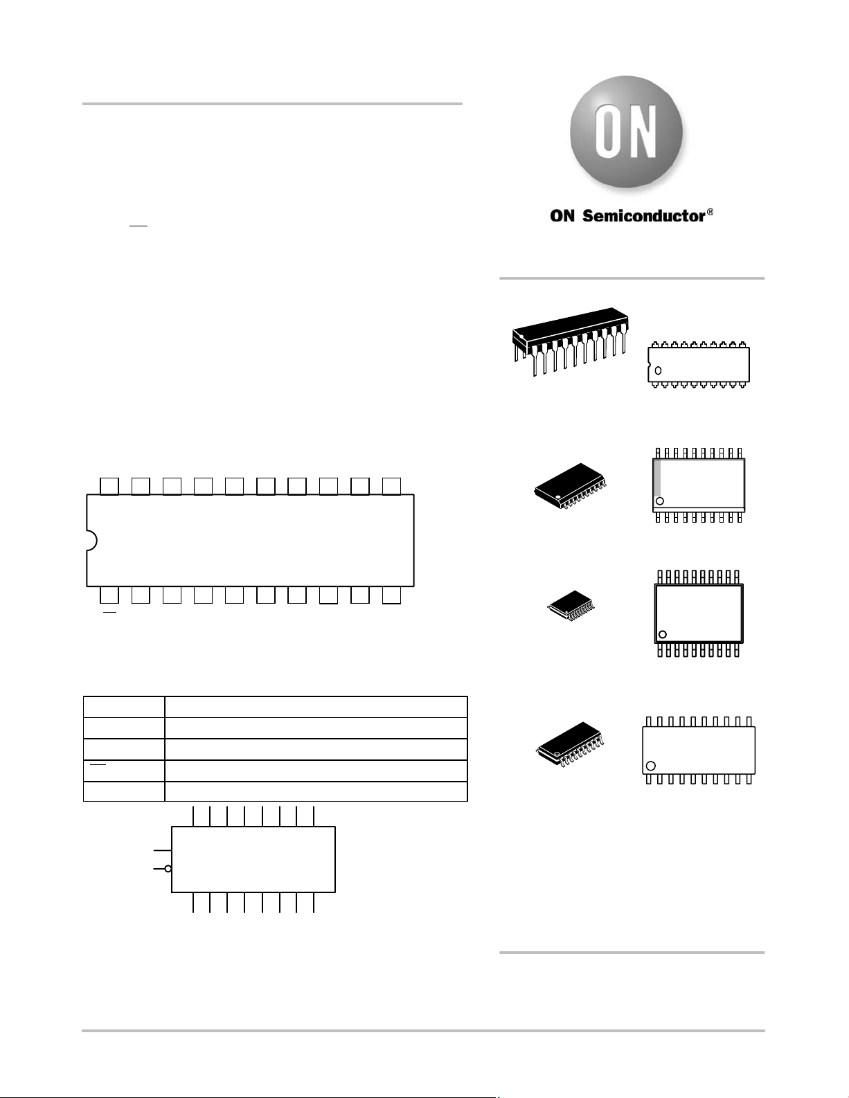
O
V
CC
0O1O2O3O4O5O6O7
1920 18 17 16 15 14
21 34567
OE
D0D1D2D3D4D5D6D7GND
13
8
Figure 1. Pinout 20−Lead Packages Conductors
(Top View)
PIN ASSIGNMENT
PIN FUNCTION
D0−D
7
LE Latch Enable Input
OE 3−State Output Enable Input
O0−O
7
Data Inputs
3−State Latch Outputs
D0D1D2D3D4D5D6D
LE
OE
O
O
1O2O3O4O5O6O7
0
7
Figure 2. Logic Symbol
*For additional information on our Pb−Free strategy and soldering details, please
download the ON Semiconductor Soldering and Mounting Techniques
Reference Manual, SOLDERRM/D.
LE
12
11
9
10
MARKING
DIAGRAM
20
1
PDIP−20
N SUFFIX
CASE 738
20
1
SO−20
DW SUFFIX
CASE 751D
20
1
TSSOP−20
DT SUFFIX
CASE 948E
20
1
EIAJ−20
M SUFFIX
CASE 967
xxx = AC or ACT
A = Assembly Location
WL, L = Wafer Lot
YY, Y = Year
WW, W = Work Week
G or G = Pb−Free Package
(Note: Microdot may be in either location)
MC74xxx573N
AWLYYWWG
xxx573
AWLYYWWG
xxx
573
ALYW G
G
74xxx573
AWLYWWG
ORDERING INFORMATION
See detailed ordering and shipping information in the package
dimensions section on page 8 of this data sheet.
© Semiconductor Components Industries, LLC, 2005
September, 2005 − Rev. 7
1 Publication Order Number:
MC74AC573/D
Page 2
MC74AC573, MC74ACT573
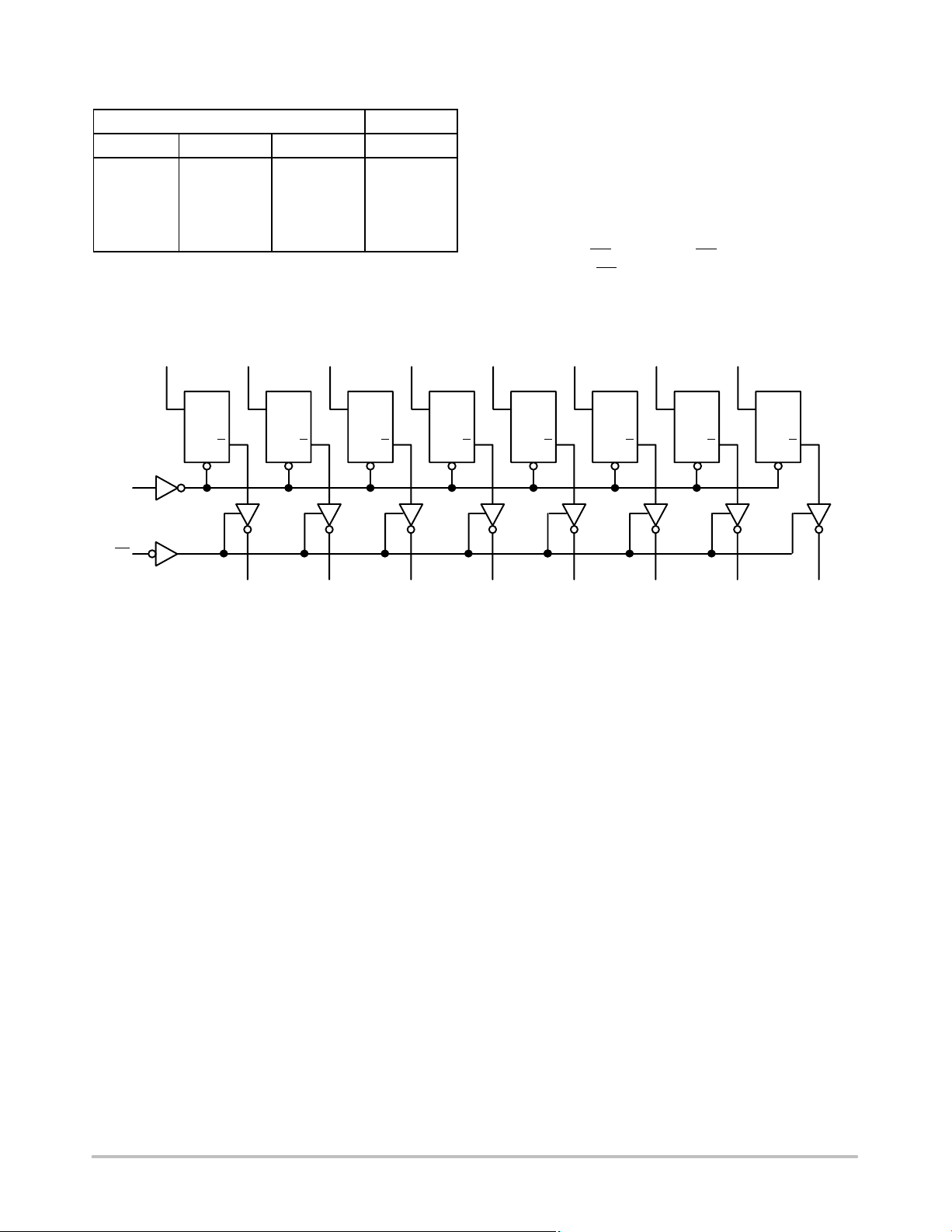
TRUTH TABLE
Inputs Outputs
OE LE D
L H H H
L H L L
L L X O
H X X Z
H = HIGH Voltage Level
L = LOW Voltage Level
Z = High Impedance
X = Immaterial
O
= Previous O0 before LOW−to−HIGH Transition of Clock
0
LE
D
1
D
Q
LE
D
0
D
LE
n
D
2
D
Q
LE
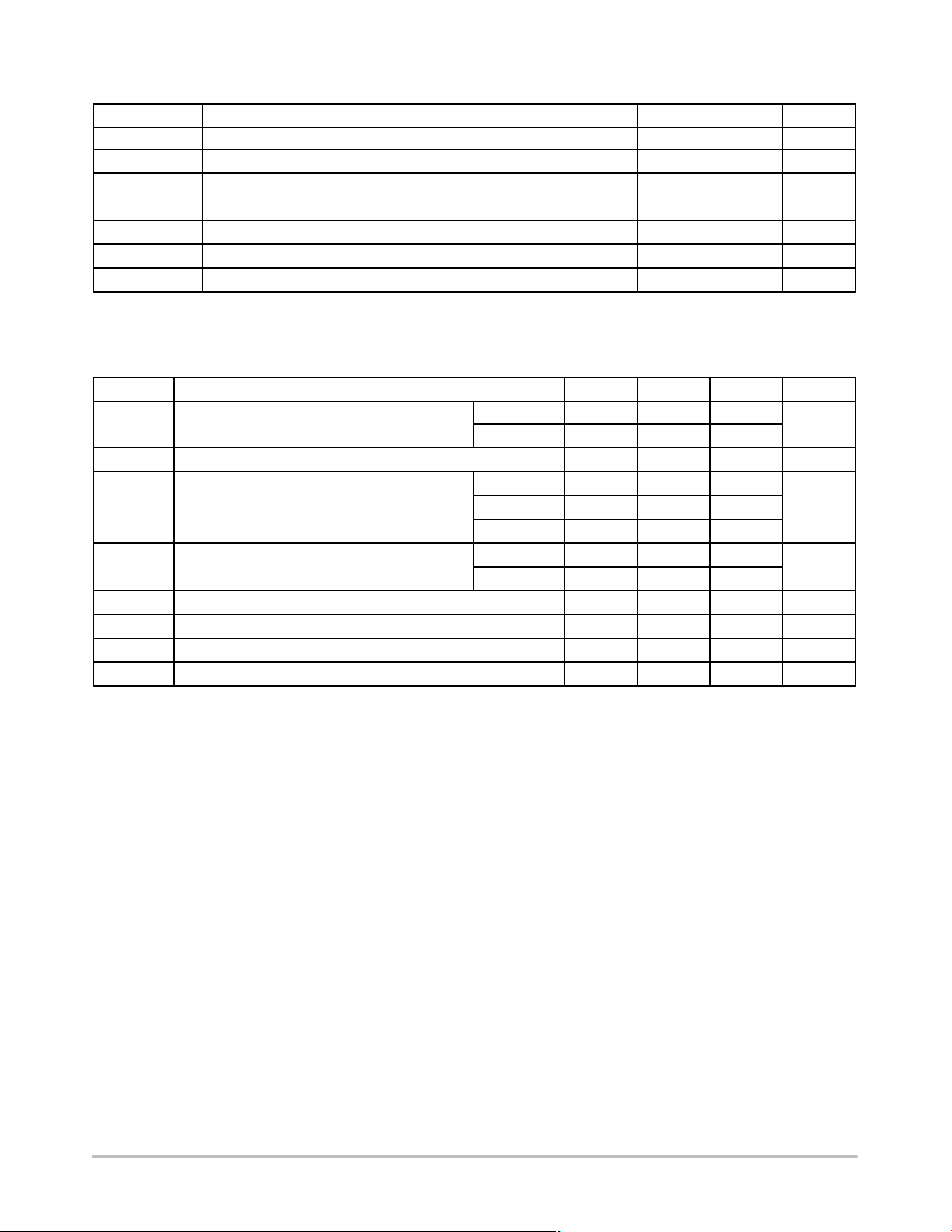
Functional Description
The MC74AC573/74ACT574 contains eight D−type
latches with 3−state output buffers. When the Latch Enable
O
n
(LE) input is HIGH, data on the D
inputs enters the latches.
n
In this condition the latches are transparent, i.e., a latch
output will change state each time its D input changes. When
LE is LOW the latches store the information that was present
0
on the D inputs a setup time preceding the HIGH−to−LOW
transition of LE. The 3−state buffers are controlled by the
Output Enable (OE
enabled. When OE
) input. When OE is LOW, the buffers are
is HIGH the buffers are in the high
impedance mode but this does not interfere with entering
new data into the latches.
D
3
D
Q
LE
D
4
D
Q
LE
D
5
D
Q
LE
D
6
D
Q
LE
D
7
D
Q
LE
Q
OE
O
0
NOTE: That this diagram is provided only for the understanding of logic
O
1
operations and should not be used to estimate propagation delays.
O
2
O
3
O
4
Figure 3. Logic Diagram
O
5
O
6
O
7
http://onsemi.com
2
Page 3
MC74AC573, MC74ACT573
MAXIMUM RATINGS
Symbol Parameter Value Unit
V
CC
V
IN
V
OUT
I
IN
I
OUT
I
CC
T
stg
Maximum ratings are those values beyond which device damage can occur. Maximum ratings applied to the device are individual stress limit
values (not normal operating conditions) and are not valid simultaneously . If these limits are exceeded, device functional operation is not implied,
damage may occur and reliability may be affected.
RECOMMENDED OPERATING CONDITIONS
Symbol Parameter Min Typ Max Unit
V
CC
VIN, V
OUT
tr, t
f
tr, t
f
T
J
T
A
I
OH
I
OL
1. VIN from 30% to 70% VCC; see individual Data Sheets for devices that differ from the typical input rise and fall times.
from 0.8 V to 2.0 V; see individual Data Sheets for devices that differ from the typical input rise and fall times.
2. V
IN
DC Supply Voltage (Referenced to GND) −0.5 to +7.0 V
DC Input Voltage (Referenced to GND) −0.5 to VCC +0.5 V
DC Output Voltage (Referenced to GND) −0.5 to VCC +0.5 V
DC Input Current, per Pin ±20 mA
DC Output Sink/Source Current, per Pin ±50 mA
DC VCC or GND Current per Output Pin ±50 mA
Storage Temperature −65 to +150 °C
Supply Voltage
DC Input Voltage, Output Voltage (Ref. to GND) 0 − V
′AC 2.0 5.0 6.0
′ACT 4.5 5.0 5.5
CC
V
V
VCC @ 3.0 V − 150 −
Input Rise and Fall Time (Note 1)
′AC Devices except Schmitt Inputs
VCC @ 4.5 V − 40 − ns/V
VCC @ 5.5 V − 25 −
Input Rise and Fall Time (Note 2)
′ACT Devices except Schmitt Inputs
VCC @ 4.5 V − 10 −
VCC @ 5.5 V − 8.0 −
ns/V
Junction Temperature (PDIP) − − 140 °C
Operating Ambient Temperature Range −40 25 85 °C
Output Current − High − − −24 mA
Output Current − Low − − 24 mA
http://onsemi.com
3
Page 4
MC74AC573, MC74ACT573
DC CHARACTERISTICS
74AC 74AC
V
CC
Symbol Parameter
(V)
TA = +25°C
Typ Guaranteed Limits
V
IH
Minimum High Level
Input Voltage
3.0 1.5 2.1 2.1 V
4.5 2.25 3.15 3.15 V or VCC − 0.1 V
5.5 2.75 3.85 3.85
V
IL
Maximum Low Level
Input Voltage
3.0 1.5 0.9 0.9 V
4.5 2.25 1.35 1.35 V or VCC − 0.1 V
5.5 2.75 1.65 1.65
V
OH
Minimum High Level
Output Voltage
3.0 2.99 2.9 2.9
4.5 4.49 4.4 4.4 V
5.5 5.49 5.4 5.4
3.0 − 2.56 2.46 −12 mA
4.5 − 3.86 3.76 I
5.5 − 4.86 4.76 −24 mA
V
OL
Maximum Low Level
Output Voltage
3.0 0.002 0.1 0.1
4.5 0.001 0.1 0.1 V
5.5 0.001 0.1 0.1
3.0 − 0.36 0.44 12 mA
4.5 − 0.36 0.44 I
5.5 − 0.36 0.44 24 mA
I
IN
I
OZ
Maximum Input
Leakage Current
Maximum
3−State
5.5 − ±0.1 ±1.0
5.5 − ±0.5 ±5.0
Current
I
OLD
I
OHD
I
CC
†Minimum Dynamic
Output Current
Maximum Quiescent
Supply Current
5.5 − − 75 mA V
5.5 − − −75 mA V
5.5 − 8.0 80
NOTE: IIN and ICC @ 3.0 V are guaranteed to be less than or equal to the respective limit @ 5.5 V VCC.
*All outputs loaded; thresholds on input associated with output under test.
†Maximum test duration 2.0 ms, one output loaded at a time.
TA =
−40°C to
+85°C
Unit Conditions
= 0.1 V
OUT
= 0.1 V
OUT
I
= −50 mA
OUT
*VIN = VIL or V
V
OH
I
OUT
−24 mA
= 50 mA
*VIN = VIL or V
mA
mA
V
OL
VI = VCC, GND
V
(OE) = VIL, V
I
VI = VCC, GND
24 mA
VO = VCC, GND
= 1.65 V Max
OLD
= 3.85 V Min
OHD
mA
VIN = VCC or GND
IH
IH
IH
http://onsemi.com
4
Page 5

MC74AC573, MC74ACT573
AC CHARACTERISTICS (For Figures and Waveforms − See Section 3)
Symbol Parameter
t
PLH
t
PHL
t
PLH
t
PHL
t
PZH
t
PZL
t
PHZ
t
PLZ
Propagation Delay
Dn to O
n
Propagation Delay
Dn to O
n
Propagation Delay
LE to O
n
Propagation Delay
LE to O
n
Output Enable Time
Output Enable Time
Output Disable Time
Output Disable Time
*Voltage Range 3.3 V is 3.3 V ±0.3 V.
Voltage Range 5.0 V is 5.0 V ±0.5 V.
VCC*
(V)
Min Typ Max Min Max
3.3 2.5 − 13.0 2.0 15.0
5.0 2.5 − 10.0 2.0 11.5
3.3 2.5 − 12.0 2.0 14.0
5.0 2.5 − 9.5 2.0 11.0
3.3 2.5 − 13.0 2.0 15.0
5.0 2.5 − 9.5 2.0 11.0
3.3 2.5 − 12.0 2.0 14.0
5.0 2.5 − 8.5 2.0 10.0
3.3 2.5 − 11.0 2.0 12.0
5.0 2.5 − 9.0 2.0 10.0
3.3 2.5 − 11.0 2.0 12.5
5.0 2.5 − 8.5 2.0 9.5
3.3 2.5 − 12.5 2.0 13.5
5.0 2.5 − 11.0 2.0 12.0
3.3 2.5 − 9.5 2.0 10.5
5.0 2.5 − 8.0 2.0 9.0
74AC 74AC
TA = +25°C
C
= 50 pF
L
TA = −40°C
C
to +85°C
= 50 pF
L
Unit
ns 3−5
ns 3−5
ns 3−6
ns 3−6
ns 3−7
ns 3−8
ns 3−7
ns 3−8
Fig.
No.
AC OPERATING REQUIREMENTS
Symbol Parameter
t
s
t
h
t
w
*Voltage Range 3.3 V is 3.3 V ±0.3 V.
Voltage Range 5.0 V is 5.0 V ±0.5 V.
Setup Time, HIGH or LOW 3.3 − 3.5 4.0
Dn to LE 5.0 − 3.0 3.5
Hold Time, HIGH or LOW 3.3 − 2.0 2.0
Dn to LE 5.0 − 2.0 2.0
LE Pulse Width, HIGH
74AC 74AC
VCC*
(V)
TA = +25°C
C
= 50 pF
L
TA = −40°C
to +85°C
C
= 50 pF
L
Typ Guaranteed Minimum
3.3 − 6.0 7.0
5.0 − 4.0 5.0
Unit
ns 3−9
ns 3−9
ns 3−6
Fig.
No.
http://onsemi.com
5
Page 6

MC74AC573, MC74ACT573
DC CHARACTERISTICS
74ACT 74ACT
V
CC
Symbol Parameter
V
IH
Minimum High Level
Input Voltage
V
IL
Maximum Low Level
Input Voltage
V
OH
Minimum High Level
Output Voltage
(V)
4.5 1.5 2.0 2.0
5.5 1.5 2.0 2.0 or VCC − 0.1 V
4.5 1.5 0.8 0.8
5.5 1.5 0.8 0.8 or VCC − 0.1 V
4.5 4.49 4.4 4.4
5.5 5.49 5.4 5.4
4.5 − 3.86 3.76 V
5.5 − 4.86 4.76 −24 mA
V
OL
Maximum Low Level
Output Voltage
4.5 0.001 0.1 0.1
5.5 0.001 0.1 0.1
4.5 − 0.36 0.44 V
5.5 − 0.36 0.44 24 mA
I
IN
DI
CCT
I
OZ
Maximum Input
Leakage Current
5.5 − ±0.1 ±1.0
Additional Max. ICC/Input 5.5 0.6 − 1.5 mA VI = VCC − 2.1 V
Maximum
3-State
5.5 − ±0.5 ±5.0
Current
I
OLD
I
OHD
I
CC
†Minimum Dynamic
Output Current
Maximum Quiescent
Supply Current
5.5 − − 75 mA V
5.5 − − −75 mA V
5.5 − 8.0 80
*All outputs loaded; thresholds on input associated with output under test.
†Maximum test duration 2.0 ms, one output loaded at a time.
AC CHARACTERISTICS (For Figures and Waveforms − See Section 3)
Symbol Parameter
t
PLH
t
PHL
t
PLH
t
PHL
t
PZH
t
PZL
t
PHZ
t
PLZ
*Voltage Range 5.0 V is 5.0 V ±0.5 V.
Propagation Delay
D
to O
n
n
Propagation Delay
D
to O
n
n
Propagation Delay
LE to O
n
Propagation Delay
LE to O
n
Output Enable Time 5.0 2.0 − 10 1.5 11 ns 3−7
Output Enable Time 5.0 1.5 − 9.5 1.5 10.5 ns 3−8
Output Disable Time 5.0 2.5 − 11 1.5 12.5 ns 3−7
Output Disable Time 5.0 1.5 − 8.5 1.0 9.5 ns 3−8
TA = +25°C
Typ Guaranteed Limits
VCC*
(V)
Min Typ Max Min Max
5.0 2.5 − 10.5 2.0 12 ns 3−5
5.0 2.5 − 10.5 2.0 12 ns 3−5
5.0 3.0 − 10.5 2.5 12 ns 3−6
5.0 2.5 − 9.5 2.0 10.5 ns 3−6
TA =
−40°C to
Unit Conditions
+85°C
74ACT 74ACT
TA = +25°C
C
= 50 pF
L
TA = −40°C
to +85°C
C
L
V
V
V
V
mA
mA
mA
= 50 pF
V
= 0.1 V
OUT
V
= 0.1 V
OUT
I
= −50 mA
OUT
*VIN = VIL or V
I
OH
I
= 50 mA
OUT
*VIN = VIL or V
I
OL
IH
−24 mA
IH
24 mA
VI = VCC, GND
V
(OE) = VIL, V
I
IH
VI = VCC, GND
VO = VCC, GND
= 1.65 V Max
OLD
= 3.85 V Min
OHD
VIN = VCC or GND
Unit
Fig.
No.
http://onsemi.com
6
Page 7

AC OPERATING REQUIREMENTS
Symbol Parameter
t
s
t
h
t
w
Setup Time, HIGH or LOW
to LE
D
n
Hold Time, HIGH or LOW
to LE
D
n
LE Pulse Width, HIGH 5.0 − 3.5 4.0 ns 3−6
*Voltage Range 5.0 V is 5.0 V ±0.5 V.
CAPACITANCE
Symbol Parameter
C
IN
C
PD
Input Capacitance 5.0 pF VCC = 5.0 V
Power Dissipation Capacitance 25 pF VCC = 5.0 V
MC74AC573, MC74ACT573
74ACT 74ACT
VCC*
(V)
5.0 − 3.0 3.5 ns 3−9
5.0 − 0 0 ns 3−9
TA = +25°C
C
= 50 pF
L
Typ Guaranteed Minimum
Value
Typ
TA = −40°C
to +85°C
= 50 pF
C
L
Unit
Unit Test Conditions
Fig.
No.
http://onsemi.com
7
Page 8

MC74AC573, MC74ACT573
ORDERING INFORMATION
Device Package Shipping
MC74AC573N PDIP−20 18 Units / Rail
MC74AC573NG PDIP−20
(Pb−Free)
MC74AC573DW SOIC−20 38 Units / Rail
MC74AC573DWG SOIC−20
(Pb−Free)
MC74AC573DWR2 SOIC−20 1000 Units / Tape & Reel
MC74AC573DWR2G SOIC−20
(Pb−Free)
MC74AC573DTR2 TSSOP−20* 2500 Units / Tape & Reel
MC74AC573DTR2G TSSOP−20* 2500 Units / Tape & Reel
MC74AC573MEL SOEIAJ−20 2000 Units / Tape & Reel
MC74AC573MELG SOEIAJ−20
(Pb−Free)
MC74ACT573N PDIP−20 18 Units / Rail
MC74ACT573NG PDIP−20
(Pb−Free)
MC74ACT573DW SOIC−20 38 Units / Rail
MC74ACT573DWG SOIC−20
(Pb−Free)
MC74ACT573DWR2 SOIC−20 1000 Units / Tape & Reel
MC74ACT573DWR2G SOIC−20
(Pb−Free)
MC74ACT573DTR2 TSSOP−20* 2500 Units / Tape & Reel
MC74ACT573DTR2G TSSOP−20* 2500 Units / Tape & Reel
†For information on tape and reel specifications,including part orientation and tape sizes, please refer to our Tape and Reel Packaging
Specifications Brochure, BRD8011/D.
*This package is inherently Pb−Free.
18 Units / Rail
38 Units / Rail
1000 Units / Tape & Reel
2000 Units / Tape & Reel
18 Units / Rail
38 Units / Rail
1000 Units / Tape & Reel
†
http://onsemi.com
8
Page 9

−T−
SEATING
PLANE
MC74AC573, MC74ACT573
PACKAGE DIMENSIONS
PDIP−20
N SUFFIX
20 PIN PLASTIC DIP PACKAGE
CASE 738−03
ISSUE E
−A−
20
11
B
1
10
C
L
K
M
E
FG
N
D
20 PL
0.25 (0.010) T
J
20 PL
0.25 (0.010) T
M
M
A
M
NOTES:
1. DIMENSIONING AND TOLERANCING PER ANSI
Y14.5M, 1982.
2. CONTROLLING DIMENSION: INCH.
3. DIMENSION L TO CENTER OF LEAD WHEN
FORMED PARALLEL.
4. DIMENSION B DOES NOT INCLUDE MOLD
FLASH.
DIM MIN MAX MIN MAX
A 25.66 27.171.010 1.070
B 6.10 6.600.240 0.260
C 3.81 4.570.150 0.180
D 0.39 0.550.015 0.022
E
F
G 2.54 BSC0.100 BSC
J 0.21 0.380.008 0.015
K 2.80 3.550.110 0.140
L 7.62 BSC0.300 BSC
M
B
M 0 15 0 15
N 0.51 1.010.020 0.040
MILLIMETERSINCHES
1.27 BSC0.050 BSC
1.27 1.770.050 0.070
____
H10X
M
B
M
0.25
SO−20
DW SUFFIX
20 PIN PLASTIC SOIC PACKAGE
CASE 751D−05
ISSUE G
D
20
1
B20X
M
SAS
T
0.25
18X
e
A
11
_
E
10
h X 45
B
B
A
SEATING
PLANE
A1
T
q
NOTES:
1. DIMENSIONS ARE IN MILLIMETERS.
2. INTERPRET DIMENSIONS AND TOLERANCES
PER ASME Y14.5M, 1994.
3. DIMENSIONS D AND E DO NOT INCLUDE MOLD
PROTRUSION.
4. MAXIMUM MOLD PROTRUSION 0.15 PER SIDE.
5. DIMENSION B DOES NOT INCLUDE DAMBAR
PROTRUSION. ALLOWABLE PROTRUSION SHALL
BE 0.13 TOTAL IN EXCESS OF B DIMENSION AT
MAXIMUM MATERIAL CONDITION.
MILLIMETERS
DIM MIN MAX
A 2.35 2.65
A1 0.10 0.25
B 0.35 0.49
C 0.23 0.32
D 12.65 12.95
E 7.40 7.60
e 1.27 BSC
H 10.05 10.55
L
C
h 0.25 0.75
L 0.50 0.90
q 0 7
__
http://onsemi.com
9
Page 10

MC74AC573, MC74ACT573
TSSOP−20
PACKAGE DIMENSIONS
DT SUFFIX
20 PIN PLASTIC TSSOP PACKAGE
CASE 948E−02
ISSUE B
20X REFK
S
U0.15 (0.006) T
0.10 (0.004) V
M
S
U
T
S
K
2X
L/2
L
PIN 1
IDENT
110
1120
B
JJ1
−U−
N
S
U0.15 (0.006) T
A
K1
SECTION N−N
0.25 (0.010)
M
−V−
N
F
DETAIL E
C
G
H
DETAIL E
0.100 (0.004)
−T−
SEATING
PLANE
D
NOTES:
1. DIMENSIONING AND TOLERANCING PER ANSI
Y14.5M, 1982.
2. CONTROLLING DIMENSION: MILLIMETER.
3. DIMENSION A DOES NOT INCLUDE MOLD
FLASH, PROTRUSIONS OR GATE BURRS. MOLD
FLASH OR GATE BURRS SHALL NOT EXCEED
0.15 (0.006) PER SIDE.
4. DIMENSION B DOES NOT INCLUDE
INTERLEAD FLASH OR PROTRUSION.
INTERLEAD FLASH OR PROTRUSION SHALL NOT
EXCEED 0.25 (0.010) PER SIDE.
5. DIMENSION K DOES NOT INCLUDE DAMBAR
PROTRUSION. ALLOWABLE DAMBAR
PROTRUSION SHALL BE 0.08 (0.003) TOTAL IN
EXCESS OF THE K DIMENSION AT MAXIMUM
MATERIAL CONDITION.
6. TERMINAL NUMBERS ARE SHOWN FOR
REFERENCE ONLY.
7. DIMENSION A AND B ARE TO BE
DETERMINED AT DATUM PLANE −W−.
INCHES
6.60 0.260
−W−
MILLIMETERS
DIMAMIN MAX MIN MAX
6.40 0.252
B 4.30 4.50 0.169 0.177
C 1.20 0.047
−−− −−−
D 0.05 0.15 0.002 0.006
F 0.50 0.75 0.020 0.030
G 0.65 BSC 0.026 BSC
H 0.27 0.37 0.011 0.015
J 0.09 0.20 0.004 0.008
J1 0.09 0.16 0.004 0.006
K 0.19 0.30 0.007 0.012
K1 0.19 0.25 0.007 0.010
L 6.40 BSC 0.252 BSC
M 0 8 0 8
____
http://onsemi.com
10
Page 11

MC74AC573, MC74ACT573
SOEIAJ−20
PACKAGE DIMENSIONS
M SUFFIX
20 PIN PLASTIC EIAJ PACKAGE
CASE 967−01
ISSUE O
20
110
Z
D
e
b
0.13 (0.005)
M
11
H
E
E
A
0.10 (0.004)
M
VIEW P
A
1
NOTES:
1. DIMENSIONING AND TOLERANCING PER ANSI
Y14.5M, 1982.
2. CONTROLLING DIMENSION: MILLIMETER.
3. DIMENSIONS D AND E DO NOT INCLUDE
L
E
Q
1
_
L
DETAIL P
MOLD FLASH OR PROTRUSIONS AND ARE
MEASURED AT THE PARTING LINE. MOLD FLASH
OR PROTRUSIONS SHALL NOT EXCEED 0.15
(0.006) PER SIDE.
4. TERMINAL NUMBERS ARE SHOWN FOR
REFERENCE ONLY.
5. THE LEAD WIDTH DIMENSION (b) DOES NOT
INCLUDE DAMBAR PROTRUSION. ALLOWABLE
DAMBAR PROTRUSION SHALL BE 0.08 (0.003)
TOTAL IN EXCESS OF THE LEAD WIDTH
DIMENSION AT MAXIMUM MATERIAL CONDITION.
DAMBAR CANNOT BE LOCATED ON THE LOWER
RADIUS OR THE FOOT. MINIMUM SPACE
BETWEEN PROTRUSIONS AND ADJACENT LEAD
TO BE 0.46 ( 0.018).
MILLIMETERS
c
DIM MIN MAX MIN MAX
−−− 2.05 −−− 0.081
A
A
0.05 0.20 0.002 0.008
1
0.35 0.50 0.014 0.020
b
0.18 0.27 0.007 0.011
c
12.35 12.80 0.486 0.504
D
5.10 5.45 0.201 0.215
E
1.27 BSC 0.050 BSC
e
H
7.40 8.20 0.291 0.323
E
0.50 0.85 0.020 0.033
L
L
1.10 1.50 0.043 0.059
E
M
Q
1
Z
10
0
_
0.70 0.90 0.028 0.035
−−− 0.81 −−− 0.032
0
_
INCHES
_
10
_
http://onsemi.com
11
Page 12

MC74AC573, MC74ACT573
ON Semiconductor and are registered trademarks of Semiconductor Components Industries, LLC (SCILLC). SCILLC reserves the right to make changes without further notice
to any products herein. SCILLC makes no warranty, representation or guarantee regarding the suitability of its products for any particular purpose, nor does SCILLC assume any liability
arising out of the application or use of any product or circuit, and specifically disclaims any and all liability, including without limitation special, consequential or incidental damages.
“Typical” parameters which may be provided in SCILLC data sheets and/or specifications can and do vary in different applications and actual performance may vary over time. All
operating parameters, including “Typicals” must be validated for each customer application by customer’s technical experts. SCILLC does not convey any license under its patent rights
nor the rights of others. SCILLC products are not designed, intended, or authorized for use as components in systems intended for surgical implant into the body, or other applications
intended to support or sustain life, or for any other application in which the failure of the SCILLC product could create a situation where personal injury or death may occur. Should
Buyer purchase or use SCILLC products for any such unintended or unauthorized application, Buyer shall indemnify and hold SCILLC and its officers, employees, subsidiaries, affiliates,
and distributors harmless against all claims, costs, damages, and expenses, and reasonable attorney fees arising out of, directly or indirectly, any claim of personal injury or death
associated with such unintended or unauthorized use, even if such claim alleges that SCILLC was negligent regarding the design or manufacture of the part. SCILLC is an Equal
Opportunity/Affirmative Action Employer. This literature is subject to all applicable copyright laws and is not for resale in any manner.
PUBLICATION ORDERING INFORMATION
LITERATURE FULFILLMENT:
Literature Distribution Center for ON Semiconductor
P.O. Box 61312, Phoenix, Arizona 85082−1312 USA
Phone: 480−829−7710 or 800−344−3860 Toll Free USA/Canada
Fax: 480−829−7709 or 800−344−3867 Toll Free USA/Canada
Email: orderlit@onsemi.com
N. American Technical Support: 800−282−9855 Toll Free
USA/Canada
Japan: ON Semiconductor, Japan Customer Focus Center
2−9−1 Kamimeguro, Meguro−ku, Tokyo, Japan 153−0051
Phone: 81−3−5773−3850
http://onsemi.com
ON Semiconductor Website: http://onsemi.com
Order Literature: http://www.onsemi.com/litorder
For additional information, please contact your
local Sales Representative.
MC74AC573/D
12
 Loading...