

Page 1
查询MC624供应商
MC642
PWM Fan Speed Controller
with Fault Detection
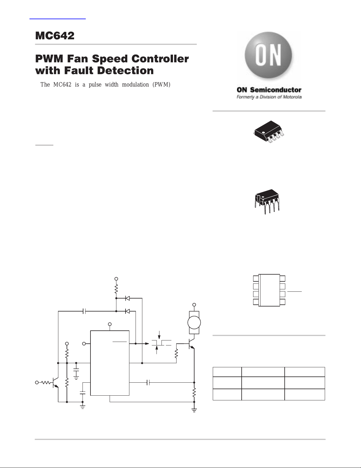
The MC642 is a pulse width modulation (PWM) fan speed
controller for use with DC motors. It provides temperature
proportional speed control. A thermistor connected to the V
furnishes the required control voltage of 1.25V to 2.65V for 0% to
100% PWM duty cycle. Minimum fan speed is set by a simple resistor
divider on the V
input. An integrated Start–Up Timer ensures
MIN
reliable motor start–up at turn–on, coming out of Shutdown Mode, or
following a transient fault. A stalled, open, or unconnected fan causes
the MC642 to trigger its start–up timer once. If the fault persists, the
FAULT
output goes low, and the device is latched in Shutdown Mode.
Features
• Shutdown Mode for Power Saving
• Supports Low Cost NTC/PTC Thermistors
• T emperature Proportional Speed for Acoustic Control /
Longer Fan Life
• Fan Voltage Independent of MC642 Supply Voltage
• Fault Detection Circuits Protect Against Fan Failure and
Aid System T esting
• Operating T emperature Range: 0°C to +85°C
Typical Applications
• Power Supplies
• Personal Computers
• UPS’s, Power Amplifiers, etc.
TYPICAL APPLICATION DIAGRAM
V
DD
D1
IN
input
+12 V
http://onsemi.com
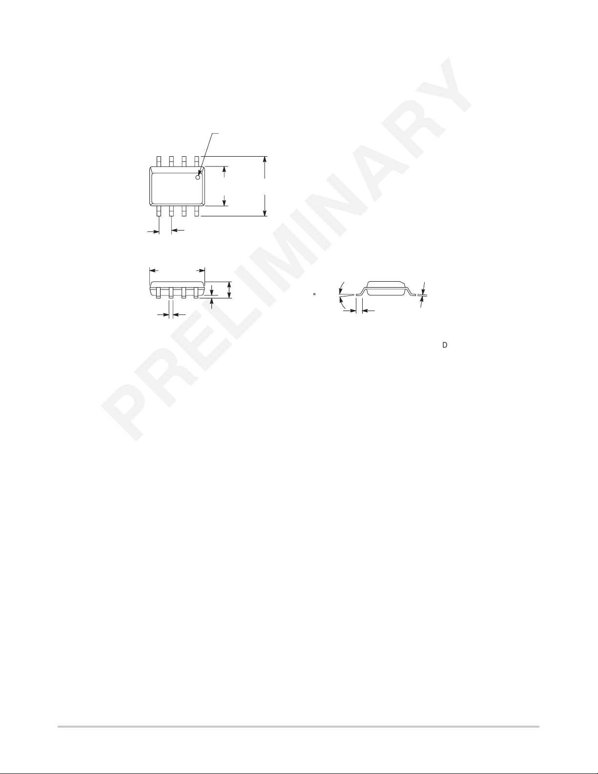
SO–8
D SUFFIX
PRELIMINARY INFORMATION
PRELIMINARY INFORMATION
CASE TBD
8–Pin DIP
P SUFFIX
CASE TBD
PIN CONFIGURATION
V
V
MIN
GND
1
IN
C
2
MC642D
F
MC642P
3
4
8
7
6
5
V
DD
V
OUT
FAULT
SENSE
+5 V
From
Temp
Sensor
V
16
8
V
DD
FAULT
in
MC642
V
min
3
C
2
(Optional)
Semiconductor Components Industries, LLC, 1999
February , 2000 – Rev. 0
+
SENSE
F
GND
4
D2
V
out
7
5
C
SENSE
MC642
Reset
1
0
Detected
Fault
FAN
Q1
R
BASE
MC642DR2 8–Pin SOIC 2500 Tape/Reel
R
SENSE
1 Publication Order Number:
MC642P 8–Pin Plastic DIP 50 Tape/Reel
ORDERING INFORMATION
Device Package Shipping
MC642/D
Page 2
V
Á
Á
Á
Á
Á
Á
Á
Á
Á
Á
Á
Á
Á
Á
Á
Á
Á
Á
MC642
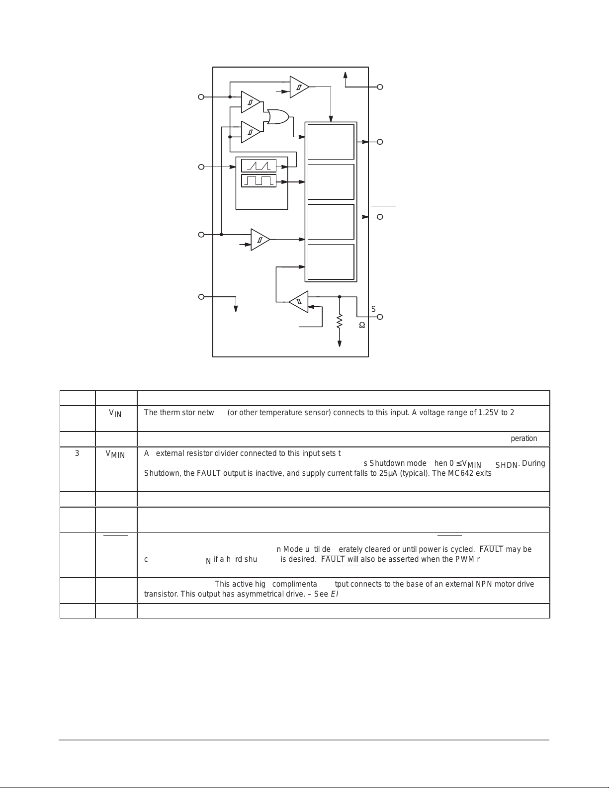
FUNCTIONAL BLOCK DIAGRAM
V
IN
C
MIN
GND
V
OTF
–
+
–
+
F
Clock
Generator
+
V
SHDN
–
MC642
70 mV (typ.)
+
–
SHDN
+
–
Control
Logic
3 X T
PWM
Timer
Start–Up
Timer
Missing
Pulse
Detector
OTF
10 k
W
V
DD
V
OUT
FAULT
SENSE
PIN DESCRIPTION
Pin No. Symbol Description
1
ÁÁ
2
3
ÁÁ
ÁÁ
4
5
6
ÁÁ
ÁÁ
7
ÁÁ
8
V
IN
Á
C
F
V
MIN
Á
Á
GND
SENSE
FAULT
Á
Á
V
OUT
Á
V
DD
The thermistor network (or other temperature sensor) connects to this input. A voltage range of 1.25V to 2.65V
(typical) on this pin drives an active duty cycle of 0% to 100% on the V
ББББББББББББББББББББББББББ
Positive terminal for the PWM ramp generator timing capacitor. The recommended CF is 1µF for 30Hz PWM operation.
An external resistor divider connected to this input sets the minimum fan speed by fixing the minimum PWM duty
cycle (1.25V to 2.65V = 0% to 100%, typical). The MC642 enters Shutdown mode when 0 ≤ V
ББББББББББББББББББББББББББ
Shutdown, the FAULT output is inactive, and supply current falls to 25µA (typical). The MC642 exits Shutdown
mode when V
ББББББББББББББББББББББББББ
MIN
≥ V
REL
. See
Applications
section for more details.
Ground Terminal
Pulses are detected at this pin as fan rotation chops the current through a sense resistor. The absence of pulses
indicates a fault.
Fault (open collector) output. This line goes low to indicate a fault condition. When FAULT goes low due to a fan
ББББББББББББББББББББББББББ
fault, the device is latched in Shutdown Mode until deliberately cleared or until power is cycled. FAULT
connected to V
ББББББББББББББББББББББББББ
cycle, however the device will not latch itself off unless FAULT
if a hard shutdown is desired. FAULT
MIN
will also be asserted when the PWM reaches 100% duty
PWM signal output. This active high complimentary output connects to the base of an external NPN motor drive
ББББББББББББББББББББББББББ
transistor. This output has asymmetrical drive. – See
Electrical Characteristics
Power Supply Input. May be independent of fan power supply. See
pin.
OUT
is tied to V
externally.
MIN
section.
Electrical Characteristics
≤ V
MIN
section.
SHDN
may be
. During
http://onsemi.com
2
Page 3
MC642
ABSOLUTE MAXIMUM RATINGS*
Parameter Value Unit
Package Power Dissipation (TA ≤ 70°C)
Plastic DIP
Small Outline (SOIC)
Derating Factors 8.0 mW/°C
Supply Voltage 6.0 V
Input Voltage, Any Pin (GND – 0.3) to (VCC + 0.3) V
Operating Temperature Range 0 to +85 °C
Maximum Chip Temperature 150 °C
Storage Temperature Range –65 to +150 °C
Lead Temperature (Soldering, 10 Seconds) +300 °C
* Maximum Ratings are those values beyond which damage to the device may occur.
ELECTRICAL CHARACTERISTICS (T
Symbol Characteristic Min Typ Max Unit
V
DD
I
DD
I
DD(SHDN)
I
IN
V
Output
OUT
t
R
t
F
t
(SHDN)
I
OL
I
OH
VIN, V
V
C(MAX)
V
C(SPAN)
V
SHDN
V
REL
Pulse–Width Modulator
F PWM Frequency (CF = 1.0µF) 26 30 34 Hz
Sense Input
V
TH(SENSE)
Fault Output
V
OL
t
MP
t
STARTUP
t
DIAG
1. Guaranteed by design, not tested.
MIN
, Inputs
, V
Supply Voltage 3.0 — 5.5 V
Supply Current, Operating
Pins 3, 5, 7 Open, CF = 1µF, VIN = V
Supply Current, Shutdown Mode
Pins 1, 5, 6, 7 Open, CF = 1µF, VIN = 0.35V
VIN, V
V
OUT
V
OUT
Pulse Width (On V
Sink Current at V
Source Current at V
Input Voltage at VIN or V
OTF
V
C(MAX)
Voltage Applied to V
Voltage Applied to V
SENSE Input Threshold Voltage with Respect to GND 50 70 90 mV
Output Low Voltage (IOH = 2.5mA) — — 0.3 Hz
Missing Pulse Detector Timeout — 32/F — Sec
Startup Time — 32/F — Sec
Diagnostic Timer Period — 3/F — Sec
Input Leakage (Note 1.)
MIN
Rise Time (IOH = 5.0mA) (Note 1.)
Fall Time (IOH = 1.0mA) (Note 1.)
, V
MIN
Specifications
HYST
OUT
DD
DD
C(MIN)
V
SHDN
VOL = 10% of V
VOH = 80% of V
– V
VDD = 5V
< TA < T
MIN
) to Clear Fault Mode
Output
Output
OUT
for 100% PWM Duty Cycle 2.5 2.65 2.8 V
MIN
to Guarantee Shutdown Mode — — VDD x 0.13 V
MIN
to Release Shutdown Mode
MIN
, VDD = 3.0V to 5.5V, unless otherwise noted.)
MAX
(CMAX)
(Note 1.)
— 0.5 1.0
— 25 —
–1.0 — 1.0 µA
— — 50 µsec
— — 50 µsec
30 — —
1.0 — —
5.0 — —
1.3 1.4 1.5 V
VDD x 0.19 — —
730
470
mW
mA
µA
µsec
mA
mA
V
http://onsemi.com
3
Page 4

MC642
DET AILED OPERATING DESCRIPTION
PWM
The PWM (Pulse Width Modulation) circuit consists of a
ramp generator and threshold detector. The frequency of the
PWM is determined by the value of the capacitor connected
to the C
input. A frequency of 30Hz is recommended (C
F
= 1µF). The PWM is also the timebase for the startup and
fault timer (see below). The PWM voltage control range is
1.25V to 2.65V (typical) for 0% to 100% output duty cycle.
V
Output
OUT
The V
pin is designed to drive a low–cost transistor or
OUT
MOSFET as the low side power switching element in the
system. V arious examples of driver circuits are shown in the
following pages. This output has asymmetric
complementary drive and is optimized for driving NPN
transistors or N–channel MOSFET’s. Since the system
relies on PWM rather than linear power control, the
dissipation in the power switch is kept to a minimum.
Generally , very small devices (TO–92 or SOT package) will
suffice. (See Output Drive Transistor Selection paragraph in
Applications Information section.)
Start–Up Timer
T o ensure reliable fan startup, the StartUp Timer turns the
V
output on for 32 cycles of the PWM whenever the fan
OUT
is started from the off–state. This occurs at power–up and
when coming out of shutdown mode. If the PWM frequency
is 30Hz (C
= 1µF), the resulting start–up time will be about
F
one second. If a Fault is detected (see below), the Diagnostic
Timer is triggered once, followed by the Startup–Up T imer .
If the fault persists, the device is shut down. See FAULT
Output below .
Shutdown Control (Optional)
When V
(pin 3) is pulled below V
MIN
, the MC642 will
SHDN
go into Shutdown mode. This can be accomplished by
driving V
with an open drain logic signal or using an
MIN
external transistor as shown in Figure 1. All functions are
suspended until the voltage on V
V
(0.85V @ VDD = 5.0V). Pulling V
REL
becomes higher than
MIN
below V
MIN
SHDN
will
always result in complete device shutdown and reset. The
FAULT output is unconditionally inactive in Shutdown
mode.
A small amount of hysteresis, typically one percent of V
(50mV at VDD = 5.0V), is designed into the V
threshold. The levels specified for V
SHDN
and V
DD
SHDN/VREL
in the
REL
Electrical Characteristics section include this hysteresis
plus adequate margin to account for normal variations in the
absolute value of the threshold and hysteresis.
CAUTION: Shutdown mode is unconditional. i.e., the
fan will not activate regardless of the voltage on V
The fan should not be shut down until all heat–producing
activity in the system is at a negligible level.)
F
SENSE Input
The SENSE input, pin 5, is connected to a low–value
current sensing resistor in the ground return leg of the fan
circuit. During normal fan operation commutation occurs as
each pole of the fan is energized. This commutation causes
brief interruptions in the fan current, which is seen as pulses
across the sense resistor. When the device is not in
Shutdown Mode and pulses are not appearing at the SENSE
input, a fault condition exists.
The short, rapid changes in fan current (high dI/dt) cause
corresponding dV/dt pulses across the sense resistor, R
The waveform on R
a logic–level pulse–train by C
is differentiated and converted to
SENSE
and the internal signal
SENSE
processing circuitry (See Figure 1). The presence and
frequency of this pulse–train is a direct indication of fan
operation. See the Applications Information section for
more details.
FAULT Output
The MC642 detects faults in two ways:
(1) Pulses appearing at SENSE due to the PWM turning on
are blanked and the remaining pulses are filtered by a
missing pulse detector. If consecutive pulses are not
detected for 32 PWM cycles (1 Sec if CF = 1µF), the
Diagnostic Timer is activated and V
OUT
continuously for three PWM cycles (100msec if CF = 1µF).
If a pulse is not detected within this window, the
Startup–Timer is triggered. This should clear a transient
fault condition. If the Missing Pulse Detector times out
again, the PWM is stopped and FAULT
goes low. When
FAULT is activated due to this condition, the device is
latched in Shutdown mode and will remain off indefinitely .
(Diodes D1, D2 and resistor R5 (See Figure 1) are provided
to ensure that fan restarting is the result of a fan fault, and not
an over–temperature fault. A CMOS logic OR gate may be
substituted for these components if available).
When F AUL T is activated due to this condition, the device
is latched in Shutdown mode and will remain off
indefinitely. Important: At this point, action must be
taken to restart the fan by momentarily pulling V
below V
, or by cycling system power. In either case
SHDN
the fan cannot be permitted to remain disabled due to a
fault condition, as severe system damage could result. If
the fan cannot be restarted, the system should be shut
down. The MC642 may be configured to continuously
attempt fan restarts if so desired.
. (Note:
IN
SENSE
is driven
MIN
.
http://onsemi.com
4
Page 5
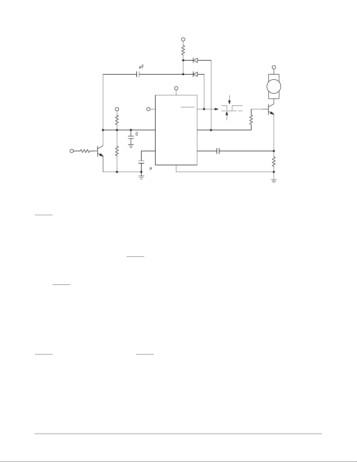
0.1 mF
MC642
V
DD
R5
10 k
D1
+12 V
From
System
Shutdown
Controller
+5 V
R1
(Optional)
* The parallel combination of R3 and R4 must be > 10 k.
R3
R4
From
Temp
Sensor
0.01
C
B
+
V
in
16
V
min
3
C
F
2
C
F
1 mF
Figure 1. T ypical Fan Control Application
Continuous restart mode is enabled by connecting the
FAULT
output to V
through a 0.1µF capacitor as shown
MIN
in Figure 1. When so connected, the MC642 automatically
attempts to restart the fan whenever a fault condition occurs.
When the fault output is driven low, the V
momentarily pulled below V
, initiating a reset and
SHDN
input is
MIN
clearing the fault condition. Normal fan startup is then
attempted as previously described. The F AUL T
output may
be connected to external logic (or the interrupt input of a
microcontroller) to shut down the MC642 if multiple fault
pulses are detected at approximately one second intervals.
(2) FAULT
is also asserted when the PWM control
voltage applied to VIN becomes greater than that needed to
drive 100% duty cycle (see Electrical Characteristics). This
indicates that the fan is at maximum drive and the potential
exists for system overheating. Either heat dissipation in the
system has gone beyond the cooling system’ s design limits
or some other fault exists such as fan bearing failure or an
airflow obstruction. This output may be treated as a System
Overheat warning and used to trigger system shutdown.
However in this case, the fan will continue to run even when
F AUL T
connected to V
is asserted. If a shutdown is desired, F AUL T may be
outside the device. This will latch the
MIN
MC642 in Shutdown Mode when any fault occurs.
8
DD
FAULT
SENSE
4
D2
V
out
7
5
MC642
Reset
1
0
Fault Detected
C
SENSE
R
BASE
FAN
Q1
R
SENSE
+5 V
V
MC642
GND
SYSTEM BEHAVIOR
The flowcharts describing the MC642’s behavioral
algorithm are shown in Figure 3. They can be summarized
as follows:
Power–Up
(1) Assuming the device is not being held in Shutdown
mode (V
> V
MIN
(2) Turn V
):
REL
output on for 32 cycles of the PWM
OUT
clock. This ensures that the fan will start from a dead stop.
(3) During this Start–up time, if a fan pulse is detected
then branch to Normal Operation; if none are received.
(4) Activate the 32–cycle Start–up Timer one more
time and look for fan pulses; if a fan pulse is detected,
proceed to Normal Operation; if none are received....
(5) Proceed to Fan Fault
(6) End
After this period elapses, the MC642 begins normal
operation.
http://onsemi.com
5
Page 6

+5 V*
MC642
R1
R2
Shutdown
(Optional)
NOTE: *See Cautions Regarding Latch–Up Considerations in the Applications Section.
R3
R4
0.01
C
B
NTC
16
3
0.01
C
B
2
+
C
F
1 mF
Figure 2. Typical Fan Control Application using NTC thermistor
Normal Operation
Normal Operation is an endless loop which may only be
exited by entering Shutdown mode or Fan Fault. The loop
can be thought of as executing at the frequency of the
oscillator and PWM.
(1) Reset the Missing Pulse Detector
(2) Is MC642 in Shutdown? If so...
a. V
duty–cycle goes to zero.
OUT
b. FAULT is disabled.
c. Exit the loop and wait for V
MIN
> V
REL
to
resume operation (indistinguishable from Power–Up).
(3) If an over–temperature fault occurs (VIN > V
then activate FAULT; release FAULT when VIN < V
(4) Drive V
of VIN and V
to a duty–cycle porportional to greater
OUT
on a cycle by cycle basis.
MIN
OTF
OTF
.
(5) If a fan pulse is detected, branch back to the start of
the loop.
(6) If the missing pulse detector times out ...
V
V
C
in
min
F
8
V
DD
MC642
SENSE
GND
4
FAULT
V
out
1 mF
C
B
7
5
C
SENSE
Thermal
Shutdown
R
BASE
+12 V
FAN
Q1
(7) Activate the 3–cycle Diagnostic Timer and look
for pulses; if a fan pulse is detected, branch back to the
start of the loop; if none are received...
(8) Activate the 32–cycle Startup Timer and look for
pulses; if a fan pulse is detected, branch back to the start of
the loop; if none are received...
(9) Quit Normal Operation and go to Fan Fault.
(10) End
Fan Fault
Fan Fault is essentially an infinite loop wherein the
MC642 is latched in Shutdown Mode. This mode can only
be released by a Reset, i.e., V
)
then above V
, or by power–cycling.
REL
being brought below V
MIN
(1) While in this state, F AULT is latched on (low), and
the V
output is disabled.
OUT
(2) A Reset sequence applied to the V
MIN
the loop to Power Up.
(3) End
R
SENSE
pin will exit
SDHN
,
http://onsemi.com
6
Page 7

Power–Up
MC642
Normal
Operation
Power–On
Reset
FAULT = 1
V< V
IN SHDN
NO
Initiate Start–
Up Timer
(1 Sec)
Fan Pulse
Detected?
YES
Normal
Operation
YES
NO
YES
Shutdown
V
= 0
OUT
Initiate Start–
Up Timer
(1 Sec)
Fan Pulse
Detected?
NO
Fan Fault
V> V
IN REL?
YES
NO
Clear
Missing Pulse
Detector
V< V
IN SHDN?
NO
YES
V> V
IN OTF?
NO
V
OUT
Proportional
T o Greater
or V
of V
IN MIN
YES NO
Fan Pulse
Detected?
YES
FAULT = 0
Shutdown
V
= 0
OUT
V> V
IN REL
YES
Power–Up
NO
Fan Fault
FAULT = Low,
V Disabled
OUT
V< V
IN SHDN?
YES
V> V
IN REL?
YES
Power–Up
NO
NO
NO
Cycling
Power?
YES
Figure 3. MC642 Behavioral Algorithm Flowchart
NO
M.P.D.
Expired?
Initiate
Diagnostic Timer
(100 mSec)
YES NO
Fan Pulse
Detected?
YES
YES
Initiate Start–
Up Timer
(1 Sec)
Fan Pulse
Detected?
NO
Fan Fault
http://onsemi.com
7
Page 8

APPLICATIONS INFORMATION
Designing with the MC642 involves the following:
(1) The temp sensor network must be configured to
deliver 1.25V to 2.65V on V
for 0% to 100% of the
IN
temperature range to be regulated.
(2) The minimum fan speed (V
) must be set.
MIN
(3) The output drive transistor and associated circuitry
must be selected.
(4) The Sense Network, R
SENSE
and C
SENSE
, must be
designed for maximum efficiency while delivering adequate
signal amplitude.
MC642
(5) If Shutdown capability is desired, the drive
requirements of the external signal or circuit must be
considered.
T emperature Sensor Design
The temperature signal connected to VIN must output a
voltage in the range of 1.25V to 2.65V (typical) for 0% to
100% of the temperature range of interest. The circuit of
Figure 4 is a convenient way to provide this signal.
V
DD
I
DIV
R1T1
I
DIV
R2
V
in
Figure 4. T emperature Sensing Circuit Figure 5. V
V
DD
FAN
R
VOH = 80% V
DD
+
V
R(BASE)
BASE
+
V
BE(SAT)
V
R(SENSE)
–
Q1
–
+
R
SENSE
–
V
OUT
SENSE
(0.1 m
R
BASE
C
SENSE
V
DD
R1
R2
GND
MIN
F Typ.)
I
IN
V
MIN
Circuit
V
FAN
DD
Q1
R
SENSE
GND
Figure 6. Circuit for Determining R
BASE
http://onsemi.com
GND
Figure 7. SENSE Network
8
Page 9

Figure 4 illustrates a simple temperature dependent
voltage divider circuit. T1 is a conventional NTC
thermistor, and R1 and R2 are standard resistors. The supply
voltage, V
, is divided between R2 and the parallel
DD
combination of T1 and R1. (For convenience, the parallel
combination of T1 and R1 will be referred to as R
TEMP
.) The
resistance of the thermistor at various temperatures is
obtained from the manufacturer’s specifications.
Thermistors are often referred to in terms of their resistance
at 25°C. A thermistor with a 25°C resistance on the order of
100kW will result in reasonable values for R1, R2, and I
DIV
In order to determine R1 and R2, we must specify the fan
duty–cycle, i.e. VIN, at any two temperatures. Equipped with
these two points on the system’s operating curve and the
thermistor data, we can write the defining equations:
VDD x R2
R
R
(t1) + R2
TEMP
VDD x R2
(t2) + R2
TEMP
Where t1 and t2 are the chosen temperatures and R
= V(t1)
= V(t2)
(1.)
TEMP
is
the parallel combination of the thermistor and R1. These
two equations permit solving for the two unknown
variables, R1 and R2. Note that resistor R1 is not absolutely
necessary, but it helps to linearize the response of the
network.
MC642
I
= 1e–4A =
DIV
R1 + R2 =
W e can further specify R1 and R2 by the condition that the
divider voltage is equal to our desired V
following equation:
.
V
MIN
Solving for the relationship between R1 and R2 results in
the following equation:
R1 = R2 x
In the case of this example, R1 = (1.762) R2. Substituting
this relationship back into Equation 4 yields the resistor
values:
R2 = 18.1kW, and
R1 = 31.9k
R1 + R2
5.0V
1e–4A
=VDD x
5.0V
VDD – V
, therefore
= 50,000W = 50k
R1
R1 + R2
MIN
V
MIN
W
. This yields the
MIN
(4.)
W
(5.)
(6.)
Minimum Fan Speed
A voltage divider on V
sets the minimum PWM duty
MIN
cycle and, thus, the minimum fan speed. As with the V
input, 1.25V to 2.65V corresponds to 0% to 100% duty
cycle. Assuming that fan speed is linearly related to
duty–cycle, the minimum speed voltage is given by the
equation:
V
MIN
Minimum Speed
=
Full Speed
x (1.4V) + 1.25V (2.)
For example, if 2500 RPM equates to 100% fan speed, and
a minimum speed of 1000 RPM is desired, then the V
MIN
voltage is:
V
MIN
The V
1000
=
2500
voltage may be set using a simple resistor
MIN
x (1.4V) + 1.25V = 1.81V (3.)
divider as shown in Figure 5. Per the Electrical
Characteristics, the leakage current at the V
pin is no
MIN
more than 1µA. It would be very conservative to design for
a divider current, I
, of 100µA. If VDD = 5.0V then...
DIV
In this case, the standard values of 32kW and 18kW are
very close to the calculated values and would be more than
IN
adequate.
One boundary condition which may impact the selection
of the minimum fan speed is the irregular activation of the
Diagnostic Timer due to the MC642 “missing” fan
commutation pulses at low speeds. Typically, this only
occurs at very low duty–cycles (25% or less). It is a natural
consequence of low PWM duty–cycles. Recall that the
SENSE function detects commutation of the fan as
disturbances in the current through R
occur when the fan is energized, i.e., V
low duty–cycles, the V
output is “off” most of the time.
OUT
. These can only
SENSE
is “on”. At very
OUT
The fan may be rotating normally, but the commutation
events are occuring during the PWM’s off–time.
The phase relationship between the fan’s commutation
and the PWM edges tends to “walk around” as the system
operates. At certain points, the MC642 may fail to capture
a pulse within the 32–cycle Missing Pulse Detector window.
When this happens, the 3–cycle Diagnostic Timer will be
activated, the V
output will be active continuously for
OUT
three cycles and, if the fan is operating normally, a pulse will
be detected. If all is well, the system will return to normal
operation. There is no harm in this behavior, but it may be
http://onsemi.com
9
Page 10

MC642
audible to the user as the fan will accelerate briefly when the
Diagnostic Timer fires. For this reason, it is recommended
that V
SENSE Network (R
be set no lower than 1.8V.
MIN
and C
SENSE
The network comprised of R
SENSE
SENSE
and C
)
SENSE
allow the
MC642 to detect commutation of the fan motor. This
network can be thought of as a differentiator and threshold
detector. The function of R
into a voltage. C
serves to AC–couple this voltage
SENSE
is to convert the fan current
SENSE
signal and provide a ground–referenced input to the SENSE
pin. Designing a proper SENSE Network is simply a matter
of scaling R
to provide the necessary amount of gain,
SENSE
i.e., the current–to–voltage conversion ratio. A 0.1µF
ceramic capacitor is recommended for C
SENSE
. Smaller
values require larger sense resistors, and higher value
capacitors are bulkier and more expensive. Using a 0.1µF
results in reasonable values for R
. Figure 7 illustrates
SENSE
a typical SENSE Network. Figure 8 shows the waveforms
observed using a typical SENSE Network.
T able 1 lists the recommended values of R
SENSE
according
to the nominal operating current of the fan. Note that the
current draw specified by the fan manufacturer may not be
the fan’s nominal operating current, but may be a worst–case
rating for near–stall conditions. The values in the table refer
to actual average operating current. If the fan current falls
between two of the values listed, use the higher resistor
value. The end result of employing T able 1 is that the signal
developed across the sense resistor is approximately 450mV
in amplitude.
Table 1. R
SENSE
vs. Fan Current
Nominal Fan Current (mA)
50 9.1
100 4.7
150 3.0
200 2.4
250 2.0
300 1.8
350 1.5
400 1.3
450 1.2
500 1.0
R
SENSE
(
W)
V
OUT
Figure 8. SENSE Waveforms
V
DD
FAN
R
R
BASE
a) Single Bipolar Transistor b) Darlington Transistor Pair c) N–Channel MOSFET
GND
Q1
R
SENSE
V
OUT
BASE
Q1
V
DD
FAN
GND
Q2
R
SENSE
V
OUT
V
DD
FAN
GND
Q1
R
SENSE
Figure 9. Output Drive Transistor Circuit Topologies
http://onsemi.com
10
Page 11

MC642
Output Drive Transistor Selection
The MC642 is designed to drive an external transistor for
modulating power to the fan. This is shown as “Q1” in
Figures 2, 6, 7, 9, 10, and 11. The V
pin has a minimum
OUT
source current of 5mA and a minimum sink current of 1mA
at V
= 5.0V . Bipolar transistors or MOSFET’ s may be used
DD
as the power switching element as shown below. When high
current gain is needed to drive larger fans, two transistors
may be used in a Darlington configuration. These circuit
topologies are shown in Figure 9: (a) shows a single NPN
transistor used as the switching element; (b) Illustrates the
Darlington pair; and (c) shows an N–channel MOSFET.
One major advantage of the MC642’s PWM control
scheme versus linear speed control is that the dissipation in
the pass element is kept very low. Generally, low–cost
devices in very small packages such as TO–92 or SOT, can
be used effectively. For fans with nominal operating
currents of no more than 200mA, a single transistor usually
suffices. Above 200mA, the Darlington or MOSFET
solution is recommended. For the fan sensing function to
work correctly it is imperative that the pass transistor be
fully saturated when “on”. The minimum gain (h
) of the
FE
transistor in question must be adequate to fully saturate the
transistor when passing the full fan current while being
driven within the 5mA IOH of the V
OUT
output.
Table 2 gives examples of some commonly available
transistors. This table is a guide only. There are many
transistor types which might work as well as those listed.
The only critical issues when choosing a device to use as Q1
are: (1) the breakdown voltage, V
, must be large
CE(BR)
enough to stand off the highest voltage applied to the fan
(NOTE: this may be when the fan is off!); (2) the gain (hFE)
must be high enough for the device to remain fully saturated
while conducting the maximum expected fan current and
being driven with no more than 5mA of base/gate drive at
maximum temperature; (3) rated fan current draw must be
within the transistor’s current handling capability; and (4)
power dissipation must be kept within the limits of the
chosen device.
Table 2. Transistors for Q1
Device V
MPS2222 1.3 100 30 150 800
MPS2222A 1.2 100 40 150 800
2N4400 0.95 50 40 150 820
2N4401 0.95 100 40 150 820
MPS6601 1.2 50 25 500 780
MPS6602 1.2 50 40 500 780
BE(SAT)
MIN hFEV
BR(CEO)IC
R
BASE
(W)
A base–current limiting resistor is required with bipolar
transistors. This is shown in Figure 6. The correct value for
this resistor can be determined as follows: (see Figure 6).
V
RSENSE
V
RBASE
I
BASE
VOH = V
= I
= R
= I
SENSE
FAN
BASE
FAN
X R
/ h
+ V
SENSE
X I
BASE
FE
BE(SAT)
+ V
RBASE
(7.)
VOH is specified as 80% of VDD in the Electrical
Characteristics table; V
datasheet. It is now possible to solve for R
R
BASE
=
VOH – V
BE(SAT)
is given in the transistor
BE(SAT)
BASE
– V
RSENSE
I
RBASE
.
(8.)
Some applications require the fan to be powered from the
negative 12V supply to keep motor noise out of the positive
voltage power supplies. As shown in Figure 10, Zener diode
D2 offsets the –12V power supply voltage holding transistor
Q1 OFF when V
is LOW. When V
OUT
is HIGH, the
OUT
voltage at the anode of D2 increases by VOH, causing Q1 to
turn ON. Operation is otherwise the same as the case of fan
operation +12V.
Latch–up Considerations
As with any CMOS IC, the potential exists for latch–up if
signals are applied to the device which are outside the power
supply range. This is of particular concern during power–up
if the external circuitry, such as the sensor network, V
MIN
divider, shutdown circuit, or fan, are powered by a supply
different from that of the MC642. Care should be taken to
ensure that the MC642’s VDD supply powers–up first. If
possible, the networks attached to VIN and V
should
MIN
connect to the VDD supply at the same physical location as
the IC itself. Even if the IC and any external networks are
powered by the same supply, physical separation of the
connecting points can result in enough parasitic capacitance
and/or inductance in the power supply connections to delay
one power supply “routing” versus another.
Power Supply Routing and Bypassing
Noise present on the VIN and V
inputs may cause
MIN
erroneous operation of the F AULT output. As a result, these
inputs should be bypassed with a 0.01µF capacitor mounted
as close to the package as possible. This is particularly true
of V
, which usually is driven from a high impedance
IN
source (such as a thermistor). In addition, the VDD input
should be bypassed with a 1µF capacitor . Grounds should be
kept as short as possible. To keep fan noise off the MC642
ground pin, individual ground returns for the MC642 and the
low side of the fan current sense resistor should be used.
http://onsemi.com
11
Page 12

V
MC642
5 V
DD
FAN
MC642
V
out
GND
Figure 10. Powering Fan From –12V Supply
Design Example (Figure 11)
Step 1. Circulate R1 and R2 based on using an NTC
having a resistance of 4.6kW at T
1.1kW at T
R1 = 75k
R2 = 1k
.
MAX
W
W
Step 2. Set minimum fan speed
V
= 1.8V
MIN
12 V
Zener
MIN
D2
and
R2
2.2 k
Q1
R4
10 k
–12 V
R3
2.2
W
Limit the divider current to 100µA from
which R5 = 33k and R6 = 18k
Step 3. Design the output circuit
Maximum fan motor current = 250mA. Q1
beta is chosen at 100 from which R7 = 1.5k
W
W
Fan
Shutdown
+5 V
R8
10 k
(Optional)
R1
R2
Q2
NTC
10 k
@ 25°C
0.01 mF
C
B
+5 V
R5
33 k
R6
+5 V
W
1 mF
+
C
B
8
V
CC
V
in
16
MC642
V
min
3
0.01
C
B
C
F
2
+
C1
1 mF
Figure 11. Design Example
4
GND
FAULT
V
out
SENSE
+12 V
FAN
System
Fault
7
5
C
SENSE
0.1 mF
R7
1.5 k
Q1
R
2.2 W
SENSE
http://onsemi.com
12
Page 13

MC642
MC642 as a Microcontroller Peripheral
(Figure 12)
In a system containing a microcontroller or other host
intelligence, the MC642 can be effectively managed as a
CPU peripheral. Routine fan control functions can be
performed by the MC642 without processor intervention.
The micro–controller receives temperature data from one or
more points throughout the system. It calculates a fan
operating speed based on an algorithm specifically designed
for the application at hand. The processor controls fan speed
using complementary port bits I/01 through I/03. Resistors
R1 through R6 (5% tolerance) form a crude 3–bit DAC that
+5 V
Open
Drain
Output
CMOS
Outputs
from One or More Sensors
Analog or Digital Temperature Data
CMOS
Microcontroller
(RESET) (Optional)
I/O
0
(MSB)
I/O
1
I/O
2
I/O
3
(LSB)
+5 V
R1
110 k
R2
240 k
R3
360 k
18 k
R5
1.5 k
R4
+5 V
R6
1 k
R7
33 k
R8
18 k
translates the 3–bit code from the processor’s outputs into a
1.6V DC control signal. (A monolithic DAC or digital pot
may be used instead of the circuit shown.)
With V
set to 1.8V, the MC642 has a minimum
MIN
operating speed of approximately 40% of full rated speed
when the processor’s output code is 000. Output codes 001
to 111 operate the fan from roughly 40% to 100% of full
speed. An open drain output from the processor can be used
to reset the MC642 following detection of a fault condition.
The FAULT
output can be connected to the processor’s
interrupt input, or to an I/O pin for polled operation.
+12 V
C
B
0.01 mF
+
1 mF
C
B
0.01 mF
+5 V
V
in
1
C
F
2
V
min
3
GND
4
MC642
FAULT
SENSE
V
DD
8
V
out
7
6
5
C
B
1 mF
+
R9
1.5 k
+5 V
R10
10 k
0.1 mF
+
FAN
–
2N2222A
R11
2.2 W
GND
INT
Figure 12. Design Example
http://onsemi.com
13
Page 14

MC642
P ACKAGE DIMENSIONS
8–Pin DIP
PLASTIC PACKAGE
CASE TBD
ISSUE TBD
PIN 1
.260 (6.60)
.240 (6.10)
.045 (1.14)
.030 (0.76)
.200 (5.08)
.140 (3.56)
.150 (3.81)
.115 (2.92)
.400 (10.16)
.348 (8.84)
.110 (2.79)
.090 (2.29)
.070 (1.78)
.045 (1.14)
.022 (0.56)
.015 (0.38)
.040 (1.02)
.020 (0.51)
.015 (0.38)
.008 (0.20)
.310 (7.87)
.290 (7.37)
3 MIN.°
.400 (10.16)
.310 (7.87)
Dimensions: inches (mm)
http://onsemi.com
14
Page 15
MC642
P ACKAGE DIMENSIONS
8–Pin SOIC
PLASTIC PACKAGE
CASE TBD
ISSUE TBD
PIN 1 indicated by dot and/or beveled edge
.050 (1.27) TYP.
.197 (5.00)
.189 (4.80)
.018 (0.46)
.014 (0.36)
.157 (3.99)
.150 (3.81)
.010 (0.25)
.004 (0.10)
.244 (6.20)
.228 (5.79)
.069 (1.75)
.053 (1.35)
_
8 MAX.
.050 (1.27)
.016 (0.40)
.010 (0.25)
.007 (0.18)
Dimensions: inches (mm)
http://onsemi.com
15
Page 16

MC642
ON Semiconductor and are trademarks of Semiconductor Components Industries, LLC (SCILLC). SCILLC reserves the right to make changes
without further notice to any products herein. SCILLC makes no warranty , representation or guarantee regarding the suitability of its products for any particular
purpose, nor does SCILLC assume any liability arising out of the application or use of any product or circuit, and specifically disclaims any and all liability ,
including without limitation special, consequential or incidental damages. “Typical” parameters which may be provided in SCILLC data sheets and/or
specifications can and do vary in different applications and actual performance may vary over time. All operating parameters, including “Typicals” must be
validated for each customer application by customer’s technical experts. SCILLC does not convey any license under its patent rights nor the rights of others.
SCILLC products are not designed, intended, or authorized for use as components in systems intended for surgical implant into the body, or other applications
intended to support or sustain life, or for any other application in which the failure of the SCILLC product could create a situation where personal injury or
death may occur. Should Buyer purchase or use SCILLC products for any such unintended or unauthorized application, Buyer shall indemnify and hold
SCILLC and its officers, employees, subsidiaries, affiliates, and distributors harmless against all claims, costs, damages, and expenses, and reasonable
attorney fees arising out of, directly or indirectly , any claim of personal injury or death associated with such unintended or unauthorized use, even if such claim
alleges that SCILLC was negligent regarding the design or manufacture of the part. SCILLC is an Equal Opportunity/Affirmative Action Employer .
PUBLICATION ORDERING INFORMATION
NORTH AMERICA Literature Fulfillment:
Literature Distribution Center for ON Semiconductor
P.O. Box 5163, Denver, Colorado 80217 USA
Phone: 303–675–2175 or 800–344–3860 Toll Free USA/Canada
Fax: 303–675–2176 or 800–344–3867 Toll Free USA/Canada
Email: ONlit@hibbertco.com
Fax Response Line: 303–675–2167 or 800–344–3810 T oll Free USA/Canada
N. American Technical Support: 800–282–9855 Toll Free USA/Canada
EUROPE: LDC for ON Semiconductor – European Support
German Phone: (+1) 303–308–7140 (M–F 1:00pm to 5:00pm Munich Time)
Email: ONlit–german@hibbertco.com
French Phone: (+1) 303–308–7141 (M–F 1:00pm to 5:00pm Toulouse T ime)
Email: ONlit–french@hibbertco.com
English Phone: (+1) 303–308–7142 (M–F 12:00pm to 5:00pm UK Time)
Email: ONlit@hibbertco.com
EUROPEAN TOLL–FREE ACCESS*: 00–800–4422–3781
*Available from Germany, France, Italy, England, Ireland
CENTRAL/SOUTH AMERICA:
Spanish Phone: 303–308–7143 (Mon–Fri 8:00am to 5:00pm MST)
Email: ONlit–spanish@hibbertco.com
ASIA/PACIFIC : LDC for ON Semiconductor – Asia Support
Phone: 303–675–2121 (T ue–Fri 9:00am to 1:00pm, Hong Kong T ime)
T oll Free from Hong Kong & Singapore:
001–800–4422–3781
Email: ONlit–asia@hibbertco.com
JAPAN: ON Semiconductor, Japan Customer Focus Center
4–32–1 Nishi–Gotanda, Shinagawa–ku, T okyo, Japan 141–8549
Phone: 81–3–5740–2745
Email: r14525@onsemi.com
ON Semiconductor Website: http://onsemi.com
For additional information, please contact your local
Sales Representative.
http://onsemi.com
16
MC642/D
 Loading...