

Page 1
MC34262, MC33262
Power Factor Controllers
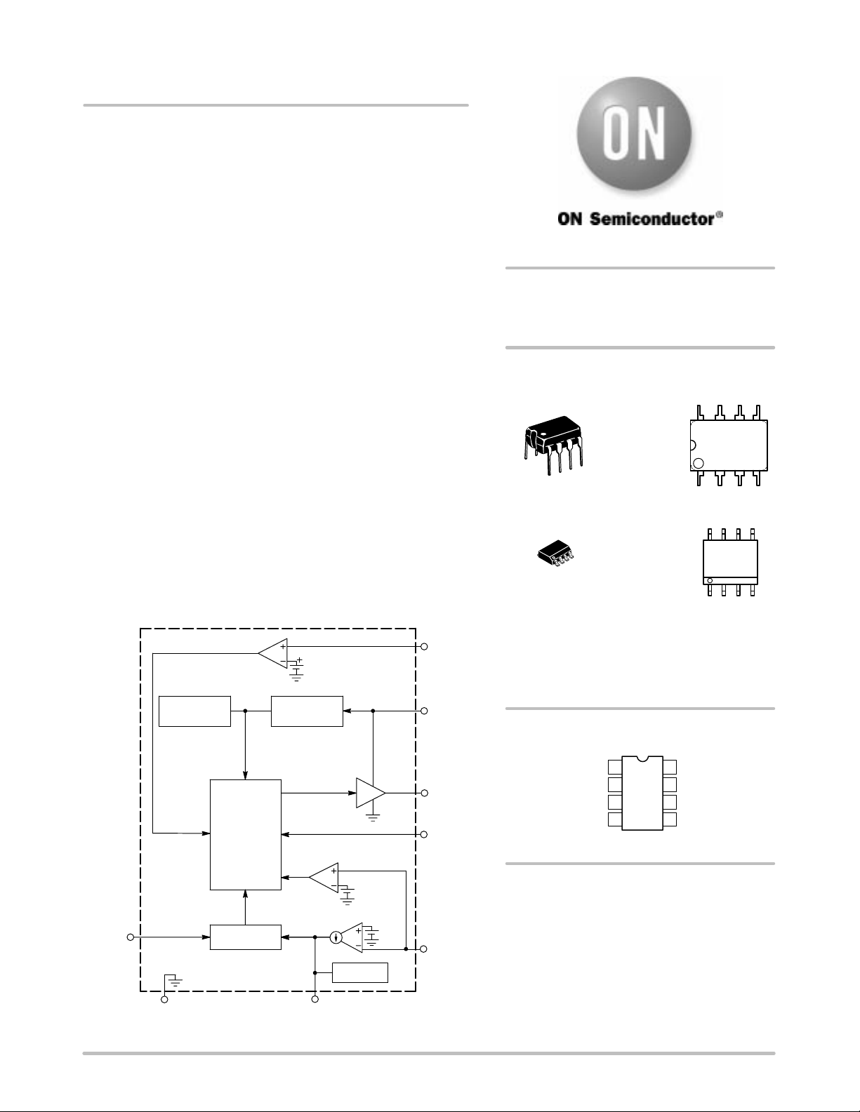
The MC34262/MC33262 are active power factor controllers
specifically designed for use as a preconverter in electronic ballast
and in off−line power converter applications. These integrated
circuits feature an internal startup timer for stand−alone applications,
a one quadrant multiplier for near unity power factor, zero current
detector to ensure critical conduction operation, transconductance
error amplifier, quickstart circuit for enhanced startup, trimmed
internal bandgap reference, current sensing comparator, and a totem
pole output ideally suited for driving a power MOSFET.
Also included are protective features consisting of an overvoltage
comparator to eliminate runaway output voltage due to load removal,
input undervoltage lockout with hysteresis, cycle−by−cycle current
limiting, multiplier output clamp that limits maximum peak switch
current, an RS latch for single pulse metering, and a drive output high
state clamp for MOSFET gate protection. These devices are
available in dual−in−line and surface mount plastic packages.
Features
• Overvoltage Comparator Eliminates Runaway Output Voltage
• Internal Startup Timer
• One Quadrant Multiplier
• Zero Current Detector
• Trimmed 2% Internal Bandgap Reference
• Totem Pole Output with High State Clamp
• Undervoltage Lockout with 6.0 V of Hysteresis
• Low Startup and Operating Current
• Supersedes Functionality of SG3561 and TDA4817
• Pb−Free Packages are Available
Zero Current Detector
2.5V
Reference
Undervoltage
Lockout
Zero Current
Detect Input
5
V
CC
8
http://onsemi.com
POWER FACTOR
CONTROLLERS
MARKING
DIAGRAMS
8
PDIP−8
P SUFFIX
8
1
8
1
CASE 626
SOIC−8
D SUFFIX
CASE 751
x = 3 or 4
A = Assembly Location
WL, L = Wafer Lot
YY, Y = Year
WW, W = Work W eek
PIN CONNECTIONS
MC3x262P
AWL
YYWW
1
8
3x262
ALYW
1
Multiplier,
Latch,
PWM,
Timer,
&
Logic
Multiplier
Input
3
6
GND
Multiplier
Compensation
Figure 1. Simplified Block Diagram
Semiconductor Components Industries, LLC, 2004
July, 2004 − Rev. 7
Error Amp
2
Overvoltage
Comparator
+
1.08 V
Quickstart
Voltage Feedback
Drive Output
7
Current Sense
Input
4
ref
+
V
ref
Voltage
Feedback
1
Input
1 Publication Order Number:
Compensation
Multiplier Input
Current Sense
ORDERING INFORMATION
See detailed ordering and shipping information in the package
dimensions section on page 17 of this data sheet.
Input
Input
1
2
3
4
(Top View)
V
8
CC
7
Drive Output
GN
6
D
Zero Current
5
Detect Input
MC34262/D
Page 2
MC34262, MC33262
MAXIMUM RATINGS
Rating Symbol Value Unit
Total Power Supply and Zener Current (ICC + IZ) 30 mA
Output Current, Source or Sink (Note 1) I
Current Sense, Multiplier, and Voltage Feedback Inputs V
Zero Current Detect Input
O
in
I
in
High State Forward Current
Low State Reverse Current
Power Dissipation and Thermal Characteristics
P Suffix, Plastic Package, Case 626
Maximum Power Dissipation @ TA = 70°C
Thermal Resistance, Junction−to−Air
P
D
R
JA
D Suffix, Plastic Package, Case 751
Maximum Power Dissipation @ TA = 70°C
Thermal Resistance, Junction−to−Air
Operating Junction Temperature T
Operating Ambient Temperature (Note 3)
P
D
R
JA
J
T
A
MC34262
MC33262
Storage Temperature T
stg
Maximum ratings are those values beyond which device damage can occur. Maximum ratings applied to the device are individual stress limit values
(not normal operating conditions) and are not valid simultaneously. If these limits are exceeded, device functional operation is not implied, damage
may occur and reliability may be affected.
500 mA
−1.0 to +10 V
mA
50
−10
800
100
450
178
mW
°C/W
mW
°C/W
+150 °C
°C
0 to + 85
− 40 to +105
− 65 to +150 °C
ELECTRICAL CHARACTERISTICS (V
= 12 V (Note 2), for typical values TA = 25°C, for min/max values T
CC
ambient temperature range that applies (Note 3), unless otherwise noted.)
Characteristic Symbol Min Typ Max Unit
ERROR AMPLIFIER
Voltage Feedback Input Threshold
TA = 25°C
TA = T
low
to T
(VCC = 12 V to 28 V)
high
Line Regulation (VCC = 12 V to 28 V , TA = 25°C) Reg
Input Bias Current (VFB = 0 V) I
Transconductance (TA = 25°C) g
Output Current
Source (VFB = 2.3 V)
Sink (VFB = 2.7 V)
Output Voltage Swing
High State (VFB = 2.3 V)
Low State (VFB = 2.7 V)
OVERVOLTAGE COMPARA TOR
Voltage Feedback Input Threshold V
MULTIPLIER
Input Bias Current, Pin 3 (V
= 0 V) I
FB
Input Threshold, Pin 2 V
1. Maximum package power dissipation limits must be observed.
2. Adjust VCC above the startup threshold before setting to 12 V .
3. T
=0°C for MC34262 T
low
= −40°C for MC33262 = +105°C for MC33262.
= +85°C for MC34262
high
V
I
V
OH(ea)
V
OL(ea)
FB(OV)
th(M)
FB
IB
O
IB
is the operating
A
V
line
2.465
2.44
− 1.0 10 mV
2.5
−
2.535
2.54
− − 0.1 − 0.5 A
m
80 100 130 mho
A
−
−
10
10
−
−
V
5.8
−
1.065 V
FB
6.4
1.7
1.08 V
FB
−
2.4
1.095 V
FB
V
− − 0.1 − 0.5 A
1.05 V
OL(EA)
1.2 V
OL(EA)
− V
http://onsemi.com
2
Page 3
MC34262, MC33262
ELECTRICAL CHARACTERISTICS (continued) (V
= 12 V (Note 5), for typical values TA = 25°C, for min/max values T
CC
operating ambient temperature range that applies (Note 6), unless otherwise noted.)
Characteristic Symbol Min Typ Max Unit
MULTIPLIER
Dynamic Input Voltage Range
Multiplier Input (Pin 3)
Compensation (Pin 2)
Multiplier Gain (V
Pin 3
= 0.5 V , V
Pin 2
= V
+ 1.0 V) (Note 7) K 0.43 0.65 0.87 1/V
th(M)
V
V
Pin 3
Pin 2
ZERO CURRENT DETECTOR
Input Threshold Voltage (Vin Increasing) V
Hysteresis (Vin Decreasing) V
th
H
Input Clamp Voltage
High State (I
Low State (I
= + 3.0 mA)
DET
= − 3.0 mA)
DET
V
IH
V
IL
CURRENT SENSE COMPARATOR
Input Bias Current (V
Input Offset V oltage (V
Maximum Current Sense Input Threshold (Note 8) V
Delay to Output t
= 0 V) I
Pin 4
Pin 2
= 1.1 V , V
= 0 V) V
Pin 3
IB
IO
th(max)
PHL(in/out)
DRIVE OUTPUT
Output Voltage (VCC = 12 V)
Low State (I
Low State (I
High State (I
High State (I
Output Voltage (VCC = 30 V)
High State (I
Output Voltage Rise T ime (CL = 1.0 nF) t
Output Voltage Fall T ime (CL = 1.0 nF) t
Output Voltage with UVLO Activated
(VCC = 7.0 V , I
= 20 mA)
Sink
= 200 mA)
Sink
= 20 mA)
Source
= 200 mA)
Source
= 20 mA, CL = 15 pF)
Source
= 1.0 mA)
Sink
V
V
V
O(max)
V
O(UVLO)
OL
OH
r
f
RESTART TIMER
Restart Time Delay t
DLY
UNDERVOLTAGE LOCKOUT
Startup Threshold (VCC Increasing) V
Minimum Operating Voltage After T urn−On (VCC Decreasing) V
Hysteresis V
th(on)
Shutdown
H
TOTAL DEVICE
Power Supply Current
I
CC
Startup (VCC = 7.0 V)
Operating
Dynamic Operating (50 kHz, CL = 1.0 nF)
Power Supply Zener Voltage (ICC = 25 mA) V
Z
4. Maximum package power dissipation limits must be observed.
5. Adjust VCC above the startup threshold before setting to 12 V .
6. T
=0°C for MC34262 T
low
= −40°C for MC33262 = +105°C for MC33262.
7. K
Pin 4 Threshold
V
Pin 3(VPin2
V
th(M )
)
8. This parameter is measured with VFB = 0 V , and V
= +85°C for MC34262
high
= 3.0 V .
Pin 3
V
(V
th(M)
0 to 2.5
th(M)
+ 1.0)
to
V
(V
th(M)
0 to 3.5
th(M)
+ 1.5)
to
−
−
1.33 1.6 1.87 V
100 200 300 mV
6.1
0.3
6.7
0.7
−
1.0
− − 0.15 −1.0 A
− 9.0 25 mV
1.3 1.5 1.8 V
− 200 400 ns
−
−
9.8
7.8
0.3
2.4
10.3
8.4
0.8
3.3
−
−
14 16 18
− 50 120 ns
− 50 120 ns
− 0.1 0.5 V
200 620 − s
11.5 13 14.5 V
7.0 8.0 9.0 V
3.8 5.0 6.2 V
−
−
−
0.25
6.5
9.0
0.4
12
20
30 36 − V
A
is the
V
V
V
V
mA
http://onsemi.com
3
Page 4
MC34262, MC33262
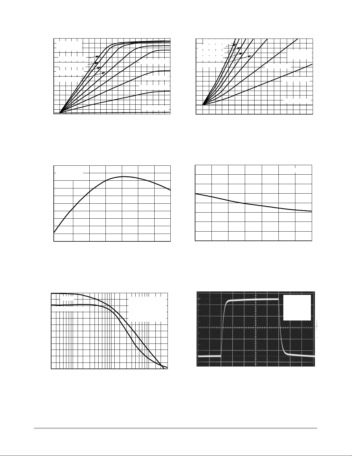
0 V/DIV
1.6 0.08
VCC = 12 V
1.4
T
= 25°C
A
1.2
V
= 3.75 V
1.0
0.8
0.6
Pin 2
V
= 3.5 V
Pin 2
V
= 3.25 V
Pin 2
V
= 3.0 V
Pin 2
V
V
Pin 2
V
Pin 2
Pin 2
= 2.75 V
= 2.5 V
= 2.25 V
0.4
0.2
, CURRENT SENSE PIN 4 THRESHOLD (V)
0
CS
1.4−0.2 3.80.6 2.2 3.0
V
Pin 2
= 2.0 V
VM, MULTIPLIER PIN 3 INPUT VOLTAGE (V)
Figure 2. Current Sense Input Threshold
versus Multiplier Input
4.0
VCC = 12 V
Pins 1 to 2
0
−4.0
−8.0
V
= 3.75 V
Pin 2
V
= 3.5 V
Pin 2
0.07
V
= 3.25 V
Pin 2
0.06
V
= 3.0 V
Pin 2
V
= 2.75 V
Pin 2
0.05
0.04
0.03
0.02
0.01
, CURRENT SENSE PIN 4 THRESHOLD (V)
0
CS
V
−0.12
−0.06 0.06 0.12 0.18 0.240
VM, MULTIPLIER PIN 3 INPUT VOLTAGE (V)
Figure 3. Current Sense Input Threshold
versus Multiplier Input, Expanded View
)
FB
110
109
108
VCC = 12 V
T
= 25°C
A
V
= 2.5 V
Pin 2
V
= 2.25 V
Pin 2
V
= 2.0 V
Pin 2
VCC = 12 V
−12
−16
, VOLTAGE FEEDBACK THRESHOLD CHANGE (mV) V
−55
FB
V
−25 0 25 50 75 100 125
T
, AMBIENT TEMPERATURE (°C)
A
Figure 4. Voltage Feedback Input Threshold
Change versus Temperature
120
100
, TRANSCONDUCTANCE (mho)
m
g
Phase
VCC = 12 V
VO = 2.5 V to 3.5 V
Transconductance
RL = 100 k to 3.0 V
CL = 2.0 pF
80
T
= 25°C
A
60
40
20
0
3.0 k 10 k 30 k 100 k 300 k 1.0 M 3.0 M
f, FREQUENCY (Hz)
107
, OVERVOLTAGE INPUT THRESHOLD (%V
106
FB(OV)
−55
V
Figure 5. Overvoltage Comparator Input
0
4.00 V
30
60
3.25 V
90
120
150
2.50 V
, EXCESS PHASE (DEGREES)
180
−25 0 25 50 75 100
T
, AMBIENT TEMPERATURE (°C)
A
Threshold versus Temperature
VCC = 12 V
RL = 100 k
CL = 2.0 pF
T
= 25°C
A
5.0 s/DIV
125
Figure 6. Error Amp Transconductance and
Phase versus Frequency
http://onsemi.com
Figure 7. Error Amp Transient Response
4
Page 5
MC34262, MC33262
0
5.0 V/DIV100 mA/DIV
1.80
VCC = 12 V
1.76
1.72
Voltage
Current
1.68
, QUICKSTART CHARGE VOLTAGE (V)
chg
V
1.64
−55 −25 0 25 50 75 100 125
T
, AMBIENT TEMPERATURE (°C)
A
Figure 8. Quickstart Charge Current
versus Temperature
1.7
Upper Threshold
(Vin, Increasing)
1.6
VCC = 12 V
900
800
700
600
500
800
VCC = 12 V
700
600
500
, RESTART TIME DELAY (s)
DLY
t
, QUICKSTART CHARGE CURRENT (A)
chg
I
400
−55
−25 0 25 50 75 100 125
T
, AMBIENT TEMPERATURE (°C)
A
Figure 9. Restart Timer Delay
versus Temperature
−2.0
−4.0
0
Source Saturation
(Load to Ground)
V
CC
VCC = 12 V
80 s Pulsed Load
120 Hz Rate
, THRESHOLD VOLTAGE (V)
th
V
90%
10%
1.5
1.4
Lower Threshold
(Vin, Decreasing)
1.3
−55
−25 0 25 50 75 100 125
T
, AMBIENT TEMPERATURE (°C)
A
Figure 10. Zero Current Detector Input
Threshold Voltage versus Temperature
VCC = 12 V
CL = 1.0 nF
T
= 25°C
A
−6.0
4.0
Sink Saturation
2.0
, OUTPUT SATURATION VOLTAGE (V)
sat
V
0
0 80 160 240 32
(Load to VCC)
GND
IO, OUTPUT LOAD CURRENT (mA)
Figure 11. Output Saturation Voltage
versus Load Current
, OUTPUT VOLTAGE
O
VCC = 12 V
CL = 15 pF
T
= 25°C
A
100 ns/DIV
CC
I
100 ns/DIV
Figure 12. Drive Output Waveform Figure 13. Drive Output Cross Conduction
http://onsemi.com
5
, SUPPLY CURRENT V
Page 6
MC34262, MC33262
16
12
8.0
VFB = 0 V
, SUPPLY CURRENT (mA)
4.0
CC
I
0
0 10203040
VCC, SUPPLY VOLTAGE (V)
Current Sense = 0 V
Multiplier = 0 V
CL = 1.0 nF
f = 50 kHz
T
= 25°C
A
Figure 14. Supply Current
versus Supply Voltage
FUNCTIONAL DESCRIPTION
Introduction
With the goal of exceeding the requirements of
legislation on line−current harmonic content, there is an
ever increasing demand for an economical method of
obtaining a unity power factor. This data sheet describes a
monolithic control IC that was specifically designed for
power factor control with minimal external components. It
offers the designer a simple, cost−effective solution to
obtain the benefits of active power factor correction.
Most electronic ballasts and switching power supplies
use a bridge rectifier and a bulk storage capacitor to derive
raw dc voltage from the utility ac line, Figure 15.
14
13
12
11
10
, SUPPLY VOLTAGE (V)
9.0
CC
V
8.0
7.0
−55 −25 0 25 50 75 100 125
Startup Threshold
(VCC Increasing)
Minimum Operating Threshold
(VCC Decreasing)
T
, AMBIENT TEMPERATURE (°C)
A
Figure 15. Undervoltage Lockout Thresholds
versus Temperature
frequency switching converter for the power processing,
with the boost converter being the most popular topology,
Figure 17. Since active input circuits operate at a frequency
much higher than that of the ac line, they are smaller,
lighter in weight, and more efficient than a passive circuit
that yields similar results. With proper control of the
preconverter, almost any complex load can be made to
appear resistive to the ac line, thus significantly reducing
the harmonic current content.
V
pk
Rectifiers Converter
AC
Line
+
Bulk
Storage
Capacitor
Load
Figure 16. Uncorrected Power Factor Circuit
This simple rectifying circuit draws power from the line
when the instantaneous ac voltage exceeds the capacitor
voltage. This occurs near the line voltage peak and results
in a high charge current spike, Figure 16. Since power is
only taken near the line voltage peaks, the resulting spikes
of current are extremely nonsinusoidal with a high content
of harmonics. This results in a poor power factor condition
where the apparent input power is much higher than the real
power. Power factor ratios of 0.5 to 0.7 are common.
Power factor correction can be achieved with the use of
either a passive or an active input circuit. Passive circuits
usually contain a combination of large capacitors,
inductors, and rectifiers that operate at the ac line
frequency. Active circuits incorporate some form of a high
Rectified
DC
0
AC Line
Voltage
0
AC Line
Current
Line Sag
Figure 17. Uncorrected Power Factor
Input Waveforms
The MC34262, MC33262 are high performance, critical
conduction, current−mode power factor controllers
specifically designed for use in off−line active
preconverters. These devices provide the necessary
features required to significantly enhance poor power
factor loads by keeping the ac line current sinusoidal and
in phase with the line voltage.
http://onsemi.com
6
Page 7

MC34262, MC33262
Operating Description
The MC34262, MC33262 contain many of the building
blocks and protection features that are employed in modern
high performance current mode power supply controllers.
There are, however, two areas where there is a major
difference when compared to popular devices such as the
Rectifiers PFC Preconverter
AC
Line
Figure 18. Active Power Factor Correction Preconverter
Error Amplifier
+
High
Frequency
Bypass
Capacitor
An Error Amplifier with access to the inverting input and
output is provided. The amplifier is a transconductance
type, meaning that it has high output impedance with
controlled voltage−to−current gain. The amplifier features
a typical gm of 100 mhos (Figure 5). The noninverting
input is internally biased at 2.5 V ± 2.0% and is not pinned
out. The output voltage of the power factor converter is
typically divided down and monitored by the inverting
input. The maximum input bias current is − 0.5 A, which
can cause an output voltage error that is equal to the product
of the input bias current and the value of the upper divider
resistor R2. The Error Amp output is internally connected
to the Multiplier and is pinned out (Pin 2) for external loop
compensation. T ypically, the bandwidth is set below 20 Hz,
so that the amplifier’s output voltage is relatively constant
over a given ac line cycle. In effect, the error amp monitors
the average output voltage of the converter over several
line cycles. The Error Amp output stage was designed to
have a relatively constant transconductance over
temperature. This allows the designer to define the
compensated bandwidth over the intended operating
temperature range. The output stage can sink and source
10 A of current and is capable of swinging from 1.7 V to
6.4 V, assuring that the Multiplier can be driven over its
entire dynamic range.
A key feature to using a transconductance type amplifier,
is that the input is allowed to move independently with
respect to the output, since the compensation capacitor is
connected to ground. This allows dual usage of of the
Voltage Feedback Input pin by the Error Amplifier and by
the Overvoltage Comparator.
Overvoltage Comparator
An Overvoltage Comparator is incorporated to eliminate
the possibility of runaway output voltage. This condition
UC3842 series. Referring to the block diagram in
Figure 19, note that a multiplier has been added to the
current sense loop and that this device does not contain an
oscillator. The reasons for these differences will become
apparent in the following discussion. A description of each
of the functional blocks is given below.
Converter
Bulk
+
MC34362
Storage
Capacitor
can occur during initial startup, sudden load removal, or
during output arcing and is the result of the low bandwidth
that must be used in the Error Amplifier control loop. The
Overvoltage Comparator monitors the peak output voltage
of the converter, and when exceeded, immediately
terminates MOSFET switching. The comparator threshold
is internally set to 1.08 V
. In order to prevent false
ref
tripping during normal operation, the value of the output
filter capacitor C3 must be large enough to keep the
peak−to−peak ripple less than 16% of the average dc
output. The Overvoltage Comparator input to Drive Output
turn−off propagation delay is typically 400 ns. A
comparison of startup overshoot without and with the
Overvoltage Comparator circuit is shown in Figure 23.
Multiplier
A single quadrant, two input multiplier is the critical
element that enables this device to control power factor.
The ac full wave rectified haversines are monitored at Pin 3
with respect to ground while the Error Amp output at Pin 2
is monitored with respect to the Voltage Feedback Input
threshold. The Multiplier is designed to have an extremely
linear transfer curve over a wide dynamic range, 0 V to
3.2 V for Pin 3, and 2.0 V to 3.75 V for Pin 2, Figure 1. The
Multiplier output controls the Current Sense Comparator
threshold as the ac voltage traverses sinusoidally from zero
to peak line, Figure 18. This has the effect of forcing the
MOSFET on−time to track the input line voltage, resulting
in a fixed Drive Output on−time, thus making the
preconverter load appear to be resistive to the ac line. An
approximation of the Current Sense Comparator threshold
can be calculated from the following equation. This
equation is accurate only under the given test condition
stated in the electrical table.
VCS, Pin 4 Threshold ≈ 0.65 (V
Pin 2
− V
th(M)
Load
) V
Pin 3
http://onsemi.com
7
Page 8

MC34262, MC33262
A significant reduction in line current distortion can be
attained by forcing the preconverter to switch as the ac line
voltage crosses through zero. The forced switching is
achieved by adding a controlled amount of offset to the
Multiplier and Current Sense Comparator circuits. The
equation shown below accounts for the built−in offsets and
is accurate to within ten percent. Let V
VCS, Pin 4 Threshold = 0.544 (V
+ 0.0417 (V
Zero Current Detector
Pin 2
Pin 2
− V
th(M)
th(M)
− V
)
th(M)
= 1.991 V
) V
Pin 3
The MC34262 operates as a critical conduction current
mode controller, whereby output switch conduction is
initiated by the Zero Current Detector and terminated when
the peak inductor current reaches the threshold level
established by the Multiplier output. The Zero Current
Detector initiates the next on−time by setting the RS Latch
at the instant the inductor current reaches zero. This critical
conduction mode of operation has two significant benefits.
First, since the MOSFET cannot turn−on until the inductor
current reaches zero, the output rectifier reverse recovery
time becomes less critical, allowing the use of an
inexpensive rectifier. Second, since there are no deadtime
gaps between cycles, the ac line current is continuous, thus
limiting the peak switch to twice the average input current.
The Zero Current Detector indirectly senses the inductor
current by monitoring when the auxiliary winding voltage
falls below 1.4 V. To prevent false tripping, 200 mV of
hysteresis is provided. Figure 9 shows that the thresholds
are well−defined over temperature. The Zero Current
Detector input is internally protected by two clamps. The
upper 6.7 V clamp prevents input overvoltage breakdown
while the lower 0.7 V clamp prevents substrate injection.
Current limit protection of the lower clamp transistor is
provided in the event that the input pin is accidentally
shorted to ground. The Zero Current Detector input to
Drive Output turn−on propagation delay is typically 320 ns.
Peak
Inductor Current
0
On
MOSFET
Q1
Off
Figure 19. Inductor Current and MOSFET
Gate Voltage Waveforms
Average
Current Sense Comparator and RS Latch
The Current Sense Comparator RS Latch configuration
used ensures that only a single pulse appears at the Drive
Output during a given cycle. The inductor current is
converted to a voltage by inserting a ground−referenced
sense resistor R7 in series with the source of output switch
Q1. This voltage is monitored by the Current Sense Input
and compared to a level derived from the Multiplier output.
The peak inductor current under normal operating
conditions is controlled by the threshold voltage of Pin 4
where:
I
L(pk
Pin 4 Threshold
) =
R
7
Abnormal operating conditions occur during
preconverter startup at extremely high line or if output
voltage sensing is lost. Under these conditions, the
Multiplier output and Current Sense threshold will be
internally clamped to 1.5 V. Therefore, the maximum peak
switch current is limited to:
I
pk(max)
1.5 V
=
R
7
An internal RC filter has been included to attenuate any
high frequency noise that may be present on the current
waveform. This filter helps reduce the ac line current
distortion especially near the zero crossings. With the
component values shown in Figure 20, the Current Sense
Comparator threshold, at the peak of the haversine varies
from 1.1 V at 90 Vac to 100 mV at 268 Vac. The Current
Sense Input to Drive Output turn−off propagation delay is
typically less than 200 ns.
Timer
A watchdog timer function was added to the IC to
eliminate the need for an external oscillator when used in
stand−alone applications. The Timer provides a means to
automatically start or restart the preconverter if the Drive
Output has been off for more than 620 s after the inductor
current reaches zero. The restart time delay versus
temperature is shown in Figure 8.
Undervoltage Lockout and Quickstart
An Undervoltage Lockout comparator has been
incorporated to guarantee that the IC is fully functional
before enabling the output stage. The positive power
supply terminal (VCC) is monitored by the UVLO
comparator with the upper threshold set at 13 V and the
lower threshold at 8.0 V. In the stand−by mode, with V
CC
at 7.0 V, the required supply current is less than 0.4 mA.
This large hysteresis and low startup current allow the
implementation of efficient bootstrap startup techniques,
making these devices ideally suited for wide input range
off−line preconverter applications. An internal 36 V
clamp has been added from VCC to ground to protect the IC
and capacitor C4 from an overvoltage condition. This
feature is desirable if external circuitry is used to delay the
startup of the preconverter. The supply current, startup, and
operating voltage characteristics are shown in Figures 13
and 14.
http://onsemi.com
8
Page 9

MC34262, MC33262
A Quickstart circuit has been incorporated to optimize
converter startup. During initial startup, compensation
capacitor C1 will be discharged, holding the error amp
output below the Multiplier threshold. This will prevent
Drive Output switching and delay bootstrapping of
capacitor C4 by diode D6. If Pin 2 does not reach the
multiplier threshold before C4 discharges below the lower
UVLO threshold, the converter will “hiccup” and
experience a significant startup delay. The Quickstart
circuit is designed to precharge C1 to 1.7 V, Figure 7. This
level is slightly below the Pin 2 Multiplier threshold,
allowing immediate Drive Output switching and bootstrap
operation when C4 crosses the upper UVLO threshold.
Drive Output
The MC34262/MC33262 contain a single totem−pole
output stage specifically designed for direct drive of power
APPLICATIONS INFORMATION
The application circuits shown in Figures 19, 20 and 21
reveal that few external components are required for a
complete power factor preconverter. Each circuit is a peak
detecting current−mode boost converter that operates in
critical conduction mode with a fixed on−time and variable
off−time. A major benefit of critical conduction operation
is that the current loop is inherently stable, thus eliminating
the need for ramp compensation. The application in
Figure 19 operates over an input voltage range of 90 Vac to
138 Vac and provides an output power of 80 W (230 V at
350 mA) with an associated power factor of approximately
MOSFETs. The Drive Output is capable of up to ±500 mA
peak current with a typical rise and fall time of 50 ns with
a 1.0 nF load. Additional internal circuitry has been added
to keep the Drive Output in a sinking mode whenever the
Undervoltage Lockout is active. This characteristic
eliminates the need for an external gate pull−down resistor.
The totem−pole output has been optimized to minimize
cross−conduction current during high speed operation. The
addition of two 10 resistors, one in series with the source
output transistor and one in series with the sink output
transistor, helps to reduce the cross−conduction current and
radiated noise by limiting the output rise and fall time. A
16 V clamp has been incorporated into the output stage to
limit the high state VOH. This prevents rupture of the
MOSFET gate when V
exceeds 20 V.
CC
0.998 at nominal line. Figures 20 and 21 are universal input
preconverter examples that operate over a continuous input
voltage range of 90 Vac to 268 Vac. Figure 20 provides an
output power of 175 W (400 V at 440 mA) while Figure 21
provides 450 W (400 V at 1.125 A). Both circuits have an
observed worst−case power factor of approximately 0.989.
The input current and voltage waveforms of Figure 20 are
shown in Figure 22 with operation at 115 Vac and 230 Vac.
The data for each of the applications was generated with the
test set−up shown in Figure 24.
http://onsemi.com
9
Page 10

MC34262, MC33262
T able 1. Design Equations
Notes Calculation
Calculate the maximum required output power. Required Converter Output Power PO = V
Calculated at the minimum required ac line voltage
for output regulation. Let the efficiency = 0.92 for
low line operation.
Let the switching cycle t = 40 s for universal input
(85 to 265 Vac) operation and 20 s for fixed input
(92 to 138 Vac, or 184 to 276 Vac) operation.
In theory the on−time ton is constant. In practice t
tends to increase at the ac line zero crossings due
to the charge on capacitor C5. Let Vac = Vac
ton and t
The off−time t
voltage and approaches zero at the ac line zero
crossings. Theta () represents the angle of the ac
line voltage.
The minimum switching frequency occurs at the peak
of the ac line voltage. As the ac line voltage traverses
from peak to zero, t
increase in switching frequency.
Set the current sense threshold VCS to 1.0 V for
universal input (85 Vac to 265 Vac) operation and
to 0.5 V for fixed input (92 Vac to 138 Vac, or
184 Vac to 276 Vac) operation. Note that VCS must
be <1.4 V.
Set the multiplier input voltage VM to 3.0 V at high
line. Empirically adjust VM for the lowest distortion
over the ac line voltage range while guaranteeing
startup at minimum line.
The IIB R1 error term can be minimized with a divider
current in excess of 50 A.
The calculated peak−to−peak ripple must be less than
16% of the average dc output voltage to prevent false
tripping of the Overvoltage Comparator. Refer to the
Overvoltage Comparator text. ESR is the equivalent
series resistance of C3.
The bandwidth is typically set to 20 Hz. When operating
at high ac line, the value of C1 may need to be
increased. (See Figure 25)
The following converter characteristics must be chosen:
calculations.
off
is greatest at the peak of the ac line
off
approaches zero producing an
off
VO − Desired output voltage
IO − Desired output current
VO − Converter output peak−to−peak ripple voltage
on
for initial
(LL)
Vac − AC RMS line voltage
Vac
− AC RMS low line voltage
(LL)
Peak Inductor Current
Inductance
Switch On−Time
Switch Off−Time
Switching Frequency
Peak Switch Current
Multiplier Input Voltage
Converter Output Voltage
Converter Output
Peak to Peak
Ripple Voltage
Error Amplifier Bandwidth
LP =
VO = V
V
t
off
O(pp)
Formula
I
=
L(pk)
V
O
t
2
ton =
=
2 Vac Sin
f =
R7 =
VM =
ref
= I
O
BW =
− Vac
2 VO P
ton + t
Vac
R
R
R
2
R
1
I
O
O
22 P
Vac
(LL)
(LL)
O
2 PO L
Vac
t
on
V
O
1
off
V
CS
I
L(pk)
2
5
+ 1
3
+ 1
1
2fac C
gm
2 C
1
O
Vac
P
2
− IIB R
3
(LL)
− 1
2
+ ESR
2
2
2
http://onsemi.com
10
Page 11

92 to
138 Vac
RFI
Filter
MC34262, MC33262
C
1
5
D
D
4
2
Zero Current
D
D
3
1
Detector
+
1.2V
+
1.6V/
36V
6.7V
1.4V
UVLO
+
16V
Drive
Output
Delay
2.5V
Reference
Timer
R
RS
Latch
13V/
8.0V
10
10
100k
R
1N4934
6
D
8
5
7
6
+
100
C
4
22k
T
R
4
MUR130
MTP
8N50E
Q
1
V
D
O
5
230V/
+
0.35A
220
C
3
0.01
C
2.2M
R
5
Current Sense
Comparator
1.5V
Overvoltage
Comparator
+
1.08 V
10A
7.5k
3
R
2
3
Multiplier
20k
10pF
ref
Error Amp
+
4
V
ref
1
Quickstart
6
2
0.68
C
1
0.1
R
1.0M
R
2
7
11k
R
1
Figure 20. 80 W Power Factor Controller
Power Factor Controller Test Data
AC Line Input DC Output
Current Harmonic Distortion (% I
V
rms
P
PF I
in
fund
THD 2357V
90 85.9 0.999 0.93 2.6 0.08 1.6 0.84 0.95 4.0 230.7 0.350 80.8 94.0
100 85.3 0.999 0.85 2.3 0.13 1.0 1.2 0.73 4.0 230.7 0.350 80.8 94.7
110 85.1 0.998 0.77 2.2 0.10 0.58 1.5 0.59 4.0 230.7 0.350 80.8 94.9
120 84.7 0.998 0.71 3.0 0.09 0.73 1.9 0.58 4.1 230.7 0.350 80.8 95.3
130 84.4 0.997 0.65 3.9 0.12 1.7 2.2 0.61 4.1 230.7 0.350 80.8 95.7
138 84.1 0.996 0.62 4.6 0.16 2.4 2.3 0.60 4.1 230.7 0.350 80.8 96.0
This data was taken with the test set−up shown in Figure 24.
= Coilcraft N2881−A
T
Primary: 62 turns of # 22 AWG
Secondary: 5 turns of # 22 AWG
Core: Coilcraft PT2510, EE 25
Gap: 0.072″ total for a primary inductance (LP) of 320 H
Heatsink
= AAVID Engineering Inc. 590302B03600, or 593002B03400
fund
)
O(pp)
V
O
I
O
P
O
(%)
http://onsemi.com
11
Page 12

90 to
268 Vac
RFI
Filter
D
D
0.01
C
MC34262, MC33262
C
1
5
D
4
2
36V
6.7V
+
1.6V/
1.2V
+
Zero Current
D
3
1
Detector
1.4V
2.5V
UVLO
Reference
Timer R
Delay
16V
Drive
Output
RS
Latch
1.3M
R
5
12k
R
2
3
Current Sense
Comparator
3
Multiplier
1.5V
Overvoltage
Comparator
+
1.08 V
10A
ref
Error Amp
Quickstart
+
+
13V/
8.0V
10
10
20k
10pF
V
100k
1N4934
R
6
D
8
5
7
4
6
+
100
C
4
22k
T
R
4
MUR460
MTP
14N50E
Q
1
V
D
O
5
400V/
+
330
0.44A
C
3
1.6M
R
2
0.1
R
7
ref
1
10k
R
1
6
2
0.68
C
1
Figure 21. 175 W Universal Input Power Factor Controller
Power Factor Controller Test Data
AC Line Input DC Output
Current Harmonic Distortion (% I
V
rms
P
PF I
in
fund
THD 2357V
90 193.3 0.991 2.15 2.8 0.18 2.6 0.55 1.0 3.3 402.1 0.44 176.9 91.5
120 190.1 0.998 1.59 1.6 0.10 1.4 0.23 0.72 3.3 402.1 0.44 176.9 93.1
138 188.2 0.999 1.36 1.2 0.12 1.3 0.65 0.80 3.3 402.1 0.44 176.9 94.0
180 184.9 0.998 1.03 2.0 0.10 0.49 1.2 0.82 3.4 402.1 0.44 176.9 95.7
240 182.0 0.993 0.76 4.4 0.09 1.6 2.3 0.51 3.4 402.1 0.44 176.9 97.2
268 180.9 0.989 0.69 5.9 0.10 2.3 2.9 0.46 3.4 402.1 0.44 176.9 97.8
This data was taken with the test set−up shown in Figure 24.
= Coilcraft N2880−A
T
Primary: 78 turns of # 16 AWG
Secondary: 6 turns of # 18 AWG
Core: Coilcraft PT4215, EE 42−15
Gap: 0.104″ total for a primary inductance (LP) of 870 H
Heatsink
= AAVID Engineering Inc. 590302B03600
fund
)
O(pp)
V
I
O
O
P
O
(%)
http://onsemi.com
12
Page 13

90 to
268 Vac
RFI
Filter
D
D
0.01
C
MC34262, MC33262
C
2
5
D
4
2
Zero Current
D
3
1
Detector
+
1.2V
+
1.6V/
36V
6.7V
1.4V
2.5V
Reference
Timer R
Delay
UVLO
+
16V
Drive
Output
RS
Latch
1.3M
R
5
12k
R
2
3
Current Sense
Comparator
3
Multiplier
1.5V
Overvoltage
Comparator
+
1.08 V
10A
ref
Error Amp
+
Quickstart
13V/
8.0V
10
10
20k
10pF
V
ref
100k
R
1N4934
6
D
+
100
C
22k
R
0.001
6
4
T
4
330
MUR460
MTW
20N50E
Q
1
V
D
O
5
400V/
+
1.125A
330
C
3
1.6M
R
2
0.05
R
7
8
5
7
4
1
10k
R
1
6
2
0.68
C
1
Figure 22. 450 W Universal Input Power Factor Controller
Power Factor Controller Test Data
AC Line Input
Current Harmonic Distortion (% I
V
rms
P
PF I
in
fund
THD 2357V
90 489.5 0.990 5.53 2.2 0.10 1.5 0.25 0.83 8.8 395.5 1.14 450.9 92.1
120 475.1 0.998 3.94 2.5 0.12 0.29 0.62 0.52 8.8 395.5 1.14 450.9 94.9
138 470.6 0.998 3.38 2.1 0.06 0.70 1.1 0.41 8.8 395.5 1.14 450.9 95.8
180 463.4 0.998 2.57 4.1 0.21 2.0 1.6 0.71 8.9 395.5 1.14 450.9 97.3
240 460.1 0.996 1.91 4.8 0.14 4.3 2.2 0.63 8.9 395.5 1.14 450.9 98.0
268 459.1 0.995 1.72 5.8 0.10 5.0 2.5 0.61 8.9 395.5 1.14 450.9 98.2
This data was taken with the test set−up shown in Figure 24.
= Coilcraft P3657−A
T
Primary: 38 turns Litz wire, 1300 strands of #48 AWG, Kerrigan−Lewis, Chicago, IL
Secondary: 3 turns of # 20 AWG
Core: Coilcraft PT4220, EE 42−20
Gap: 0.180″ total for a primary inductance (LP) of 190 H
Heatsink
= AAVID Engineering Inc. 604953B04000 Extrusion
fund
)
O(pp)
DC Output
V
O
I
P
O
O
(%)
http://onsemi.com
13
Page 14

MC34262, MC33262
Input = 115 VAC, Output = 175 W Input = 230 VAC, Output = 175 W
Voltage = 100 V/DIV
500 V
400 V
0 V
26%
Current = 1.0 A/DIV
Voltage = 100 V/DIV
2.0 ms/DIV 2.0 ms/DIV
Figure 23. Power Factor Corrected Input Waveforms
(Figure 20 Circuit)
Without Overvoltage Comparator
432 V
400 V
80 V/DIV
0 V
Current = 1.0 A/DIV
With Overvoltage Comparator
8%
80 V/DIV
200 ms/DIV200 ms/DIV
Figure 24. Output Voltage Startup Overshoot
(Figure 20 Circuit)
2X Step−Up
Line
115 Vac
Input
Neutral
Earth
Isolation
Transformer
Autoformer
AC POWER ANALYZER
PM 1000
OI
HIHI
ArmsVrmsPFVAW
53210
HARMFREQ
AinstAcfVcf
11
1397
LO
LO
VA
Voltech
0.1
RFI Test Filter
T
0.005
1.0
0.005
Figure 25. Power Factor Test Set−Up
An RFI filter is required for best performance when connecting the preconverter directly to the ac line. The filter attenuates
the level of high frequency switching that appears on the ac line current waveform. Figures 19 and 20 work well with
commercially available two stage filters such as the Delta Electronics 03DPCG5. Shown above is a single stage test filter
that can easily be constructed with four ac line rated capacitors and a common−mode transformer. Coilcraft CMT3−28−2
was used to test Figures 19 and 20. It has a minimum inductance of 28 mH and a maximum current rating of 2.0 A. Coilcraft
CMT4−17−9 was used to test Figure 21. It has a minimum inductance of 17 mH and a maximum current rating of 9.0 A. Circuit
conversion efficiency (%) was calculated without the power loss of the RFI filter.
0 to 270 Vac
Output to Power
Factor
Controller Circuit
http://onsemi.com
14
Page 15

MC34262, MC33262
Error Amp
10A
6
2
C
1
+
R
2
1
R
1
Figure 26. Error Amp Compensation
The Error Amp output is a high impedance node and is susceptible to noise pickup. To minimize pickup, compensation
capacitor C1 must be connected as close to Pin 2 as possible with a short, heavy ground returning directly to Pin 6. When
operating at high ac line, the voltage at Pin 2 may approach the lower threshold of the Multiplier, ≈ 2.0 V. If there is
excessive ripple on Pin 2, the Multiplier will be driven into cut−of f causing circuit instability, high distortion and poor power
factor . This problem can be eliminated by increasing the value of C1.
7
7
22k
10pF
Current
Sense
Comparator
4
R
C
Figure 27. Current Waveform Spike Suppression
A narrow turn−on spike is usually present on the leading edge of
the current waveform and can cause circuit instability. The
MC34262 provides an internal RC filter with a time constant of
220 ns. An additional external RC filter may be required in
universal input applications that are above 200 W. It is
suggested t h a t t h e e x t e r n a l filter be placed directly at the Current
Sense Input and have a time constant that approximates the
spike duration.
22k
R
7
Current
Sense
Comparator
10pF
4
D
1
R
7
Figure 28. Negative Current Waveform
Spike Suppression
A negative turn−off spike can be observed on the trailing edge of
the current waveform. This spike is due to the parasitic
inductance of resistor R7, and if it is excessive, it can cause
circuit instability. The addition of Schottky diode D1 can
effectively clamp the negative spike. The addition of the external
RC filter shown in Figure 26 may provide sufficient spike
attenuation.
http://onsemi.com
15
Page 16

MC34262, MC33262
(Top View)
4.5″
(Bottom View)
NOTE: Use 2 oz. copper laminate for optimum circuit performance.
Figure 29. Printed Circuit Board and Component Layout
(Circuits of Figures 20 and 21)
http://onsemi.com
16
3.0″
Page 17

MC34262, MC33262
DEVICE ORDERING INFORMATION
Device Operating Temperature Range Package Shipping
MC34262D SOIC−8 98 Units / Rail
MC34262DG
°
MC34262DR2
MC34262DR2G SOIC−8
MC34262P PDIP−8 50 Units / Rail
MC34262PG
MC33262D SOIC−8 98 Units / Rail
MC33262DG SOIC−8
MC33262DR2 SOIC−8 2500 / Tape & Reel
MC33262DR2G
MC33262P PDIP−8 50 Units / Rail
MC33262PG PDIP−8
†For information on tape and reel specifications, including part orientation and tape sizes, please refer to our Tape and Reel Packaging
Specifications Brochure, BRD8011/D.
TA = 0°C to +85°C
TA = 0°C to +85°C
TA = −40°C to +105°C
°
SOIC−8
(Pb−Free)
SOIC−8 2500 / Tape & Reel
(Pb−Free)
PDIP−8
(Pb−Free)
(Pb−Free)
SOIC−8
(Pb−Free)
(Pb−Free)
98 Units / Rail
2500 / Tape & Reel
50 Units / Rail
98 Units / Rail
2500 / Tape & Reel
50 Units / Rail
†
http://onsemi.com
17
Page 18

NOTE 2
−T−
SEATING
PLANE
H
58
−B−
14
F
−A−
C
N
D
G
0.13 (0.005) B
MC34262, MC33262
PACKAGE DIMENSIONS
PDIP−8
P SUFFIX
PLASTIC PACKAGE
CASE 626−05
ISSUE L
K
M
M
A
T
M
NOTES:
1. DIMENSION L TO CENTER OF LEAD WHEN
FORMED PARALLEL.
2. PACKAGE CONTOUR OPTIONAL (ROUND OR
SQUARE CORNERS).
3. DIMENSIONING AND TOLERANCING PER ANSI
Y14.5M, 1982.
DIM MIN MAX MIN MAX
A 9.40 10.16 0.370 0.400
B 6.10 6.60 0.240 0.260
C 3.94 4.45 0.155 0.175
D 0.38 0.51 0.015 0.020
L
J
F 1.02 1.78 0.040 0.070
G 2.54 BSC 0.100 BSC
H 0.76 1.27 0.030 0.050
J 0.20 0.30 0.008 0.012
K 2.92 3.43 0.115 0.135
L 7.62 BSC 0.300 BSC
M −−− 10 −−− 10
N 0.76 1.01 0.030 0.040
INCHESMILLIMETERS
M
http://onsemi.com
18
Page 19

MC34262, MC33262
PACKAGE DIMENSIONS
SOIC−8
D SUFFIX
PLASTIC PACKAGE
CASE 751−07
ISSUE AB
−Y−
−Z−
−X−
A
58
B
1
S
0.25 (0.010)
4
M
M
Y
K
G
N
C
SEATING
PLANE
0.10 (0.004)
H
D
0.25 (0.010) Z
M
Y
SXS
X 45
M
J
NOTES:
1. DIMENSIONING AND TOLERANCING PER
ANSI Y14.5M, 1982.
2. CONTROLLING DIMENSION: MILLIMETER.
3. DIMENSION A AND B DO NOT INCLUDE
MOLD PROTRUSION.
4. MAXIMUM MOLD PROTRUSION 0.15 (0.006)
PER SIDE.
5. DIMENSION D DOES NOT INCLUDE DAMBAR
PROTRUSION. ALLOWABLE DAMBAR
PROTRUSION SHALL BE 0.127 (0.005) TOTAL
IN EXCESS OF THE D DIMENSION AT
MAXIMUM MATERIAL CONDITION.
6. 751−01 THRU 751−06 ARE OBSOLETE. NEW
STANDARD IS 751−07.
MILLIMETERS
DIMAMIN MAX MIN MAX
4.80 5.00 0.189 0.197
B 3.80 4.00 0.150 0.157
C 1.35 1.75 0.053 0.069
D 0.33 0.51 0.013 0.020
G 1.27 BSC 0.050 BSC
H 0.10 0.25 0.004 0.010
J 0.19 0.25 0.007 0.010
K 0.40 1.27 0.016 0.050
M 0 8 0 8
N 0.25 0.50 0.010 0.020
S 5.80 6.20 0.228 0.244
INCHES
SOLDERING FOOTPRINT*
1.52
0.060
7.0
0.275
0.6
0.024
4.0
0.155
1.270
0.050
SCALE 6:1
inches
mm
*For additional information on our Pb−Free strategy and soldering
details, please download the ON Semiconductor Soldering and
Mounting Techniques Reference Manual, SOLDERRM/D.
http://onsemi.com
19
Page 20

MC34262, MC33262
The products described herein (MC34262, MC33262), may be covered by the following U.S. patent: 5,073,850. There may be other patents
pending.
ON Semiconductor and are registered trademarks of Semiconductor Components Industries, LLC (SCILLC). SCILLC reserves the right to make changes without further notice
to any products herein. SCILLC makes no warranty, representation or guarantee regarding the suitability of its products for any particular purpose, nor does SCILLC assume any
liability arising out of the application or use of any product or circuit, and specifically disclaims any and all liability, including without limitation special, consequential or incidental
damages. “Typical” parameters which may be provided in SCILLC data sheets and/or specifications can and do vary in different applications and actual performance may vary over
time. All operating parameters, including “Typicals” must be validated for each customer application by customer’s technical experts. SCILLC does not convey any license under
its patent rights nor the rights of others. SCILLC products are not designed, intended, or authorized for use as components in systems intended for surgical implant into the body,
or other applications intended to support or sustain life, or for any other application in which the failure of the SCILLC product could create a situation where personal injury or death
may occur. Should Buyer purchase or use SCILLC products for any such unintended or unauthorized application, Buyer shall indemnify and hold SCILLC and its officers, employees,
subsidiaries, affiliates, and distributors harmless against all claims, costs, damages, and expenses, and reasonable attorney fees arising out of, directly or indirectly, any claim of
personal injury or death associated with such unintended or unauthorized use, even if such claim alleges that SCILLC was negligent regarding the design or manufacture of the part.
SCILLC is an Equal Opportunity/Affirmative Action Employer. This literature is subject to all applicable copyright laws and is not for resale in any manner.
PUBLICATION ORDERING INFORMATION
LITERATURE FULFILLMENT:
Literature Distribution Center for ON Semiconductor
P.O. Box 61312, Phoenix, Arizona 85082−1312 USA
Phone: 480−829−7710 or 800−344−3860 Toll Free USA/Canada
Fax: 480−829−7709 or 800−344−3867 Toll Free USA/Canada
Email: orderlit@onsemi.com
N. American Technical Support: 800−282−9855 Toll Free
USA/Canada
Japan: ON Semiconductor, Japan Customer Focus Center
2−9−1 Kamimeguro, Meguro−ku, Tokyo, Japan 153−0051
Phone: 81−3−5773−3850
http://onsemi.com
ON Semiconductor Website: http://onsemi.com
Order Literature: http://www.onsemi.com/litorder
For additional information, please contact your
local Sales Representative.
MC34262/D
20
 Loading...