

Page 1
查询MC100210供应商
MC33178, MC33179
Low Power, Low Noise
Operational Amplifiers
The MC33178/9 series is a family of high quality monolithic
amplifiers employing Bipolar technology with innovative high
performance concepts for quality audio and data signal processing
applications. This device family incorporates the use of high
frequency PNP input transistors to produce amplifiers exhibiting low
input offset voltage, noise and distortion. In addition, the amplifier
provides high output current drive capability while consuming only
420 mA of drain current per amplifier. The NPN output stage used,
exhibits no deadband crossover distortion, large output voltage swing,
excellent phase and gain margins, low open−loop high frequency
output impedance, symmetrical source and sink AC frequency
performance.
The MC33178/9 family offers both dual and quad amplifier
versions in several package options.
Features
• 600 W Output Drive Capability
• Large Output Voltage Swing
• Low Offset Voltage: 0.15 mV (Mean)
• Low T.C. of Input Offset Voltage: 2.0 mV/°C
• Low Total Harmonic Distortion: 0.0024%
(@ 1.0 kHz w/600 W Load)
• High Gain Bandwidth: 5.0 MHz
• High Slew Rate: 2.0 V/ms
• Dual Supply Operation: ±2.0 V to ±18 V
• ESD Clamps on the Inputs Increase Ruggedness without Affecting
Device Performance
• Pb−Free Packages are Available
V
CC
http://onsemi.com
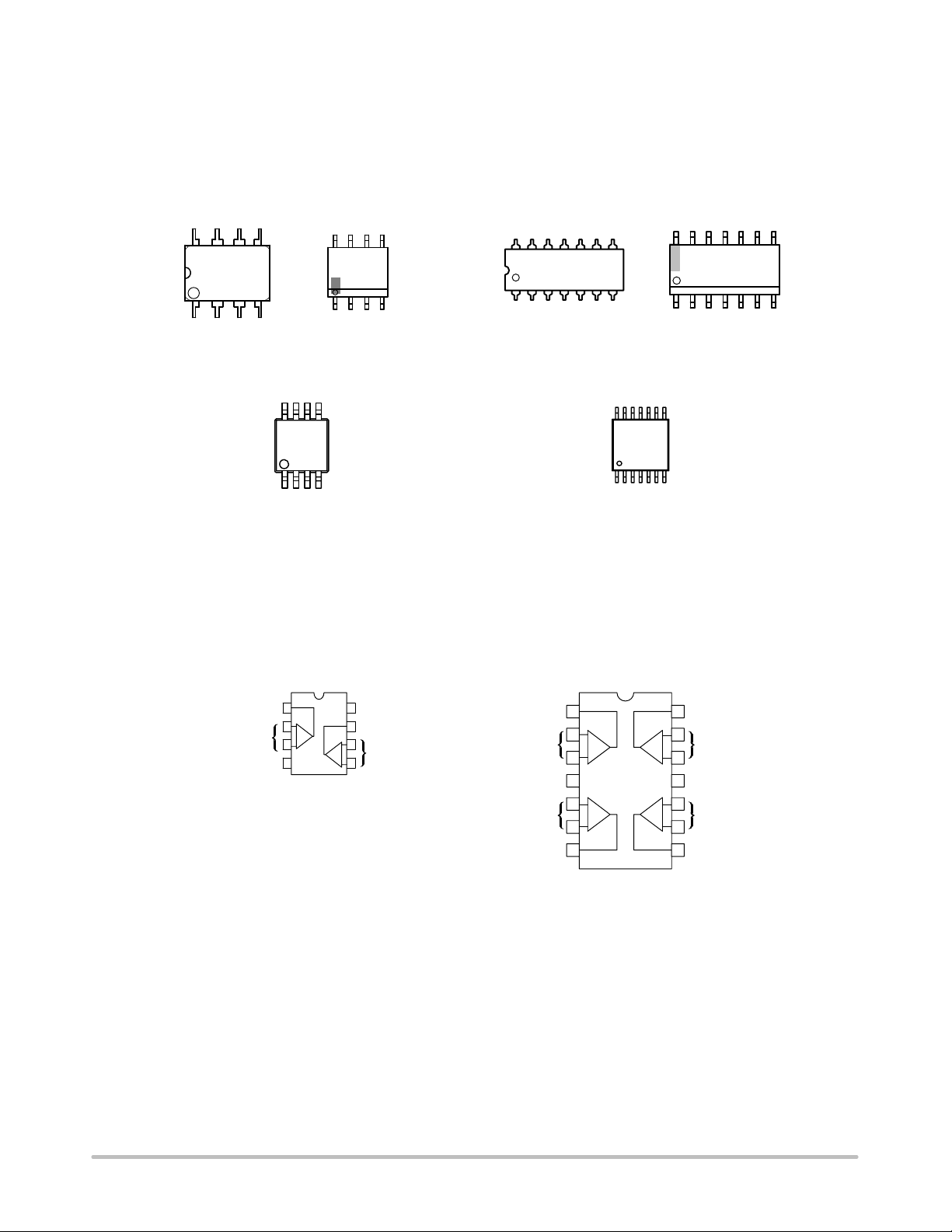
DUAL
8
1
8
1
8
1
QUAD
14
1
14
1
PDIP−8
P SUFFIX
CASE 626
SOIC−8
D SUFFIX
CASE 751
Micro8
DM SUFFIX
CASE 846A
PDIP−14
P SUFFIX
CASE 646
SOIC−14
D SUFFIX
CASE 751A
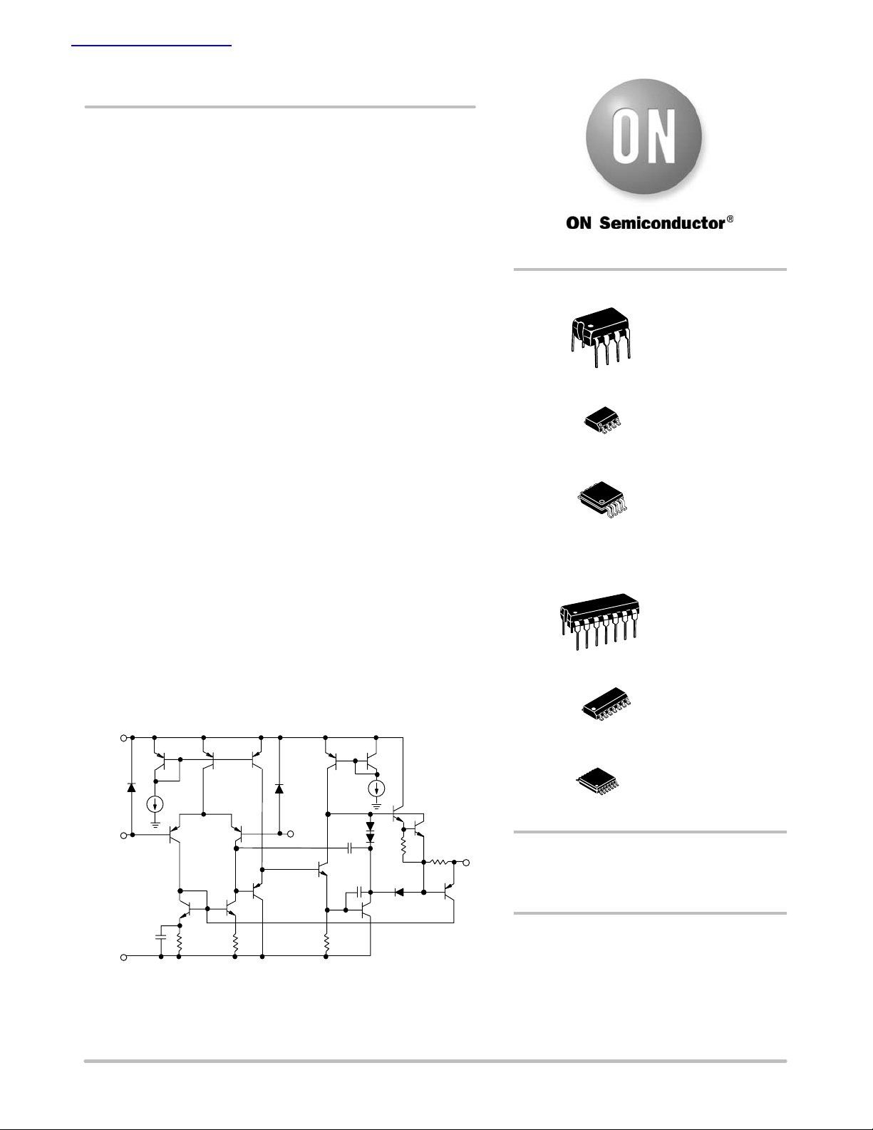
I
ref
Vin −
V
EE
Figure 1. Representative Schematic Diagram
(Each Amplifier)
© Semiconductor Components Industries, LLC, 2005
October, 2005 − Rev. 6
Vin +
I
ref
C
C
V
C
M
1 Publication Order Number:
O
14
1
ORDERING INFORMATION
See detailed ordering and shipping information in the package
dimensions section on page 2 of this data sheet.
DEVICE MARKING INFORMATION
See general marking information in the device marking
section on page 4 of this data sheet.
TSSOP−14
DTB SUFFIX
CASE 948G
MC33178/D
Page 2
MC33178, MC33179
MAXIMUM RATINGS
Rating Symbol Value Unit
Supply Voltage (VCC to V
EE)
Input Differential Voltage Range V
Input Voltage Range V
Output Short Circuit Duration (Note 2) t
Maximum Junction Temperature T
Storage Temperature Range T
Maximum Power Dissipation P
Operating Temperature Range T
Maximum ratings are those values beyond which device damage can occur. Maximum ratings applied to the device are individual stress limit
values (not normal operating conditions) and are not valid simultaneously. If these limits are exceeded, device functional operation is not implied,
damage may occur and reliability may be affected.
1. Either or both input voltages should not exceed VCC or VEE.
2. Power dissipation must be considered to ensure maximum junction temperature (TJ) is not exceeded. (See power dissipation performance
characteristic, Figure 2.)
V
IDR
IR
SC
stg
A
S
+36 V
Note 1 V
Note 1 V
Indefinite sec
J
+150 °C
−60 to +150 °C
D
Note 2 mW
−40 to +85 °C
ORDERING INFORMATION
Device Package Shipping
MC33178D SOIC−8 98 Units / Rail
MC33178DG SOIC−8
(Pb−Free)
98 Units / Rail
MC33178DR2 SOIC−8 2500 / Tape & Reel
MC33178DR2G SOIC−8
(Pb−Free)
2500 / Tape & Reel
MC33178P PDIP−8 1000 Units / Rail
MC33178PG PDIP−8
(Pb−Free)
1000 Units / Rail
MC33178DMR2 Micro8 4000 / Tape & Reel
MC33178DMR2G Micro8
(Pb−Free)
4000 / Tape & Reel
MC33179D SOIC−14 55 Units / Rail
MC33179DG SOIC−14
(Pb−Free)
55 Units / Rail
MC33179DR2 SOIC−14 2500 / Tape & Reel
MC33179DR2G SOIC−14
(Pb−Free)
2500 / Tape & Reel
MC33179P PDIP−14 500 Units / Rail
MC33179PG PDIP−14
(Pb−Free)
MC33179DTBR2G TSSOP−14
(Pb−Free)
500 Units / Rail
2500 / Tape & Reel
†For information on tape and reel specifications, including part orientation and tape sizes, please refer to our Tape and Reel Packaging
Specifications Brochure, BRD8011/D.
†
http://onsemi.com
2
Page 3
MC33178, MC33179
MARKING DIAGRAMS
DUAL QUAD
PDIP−8
CASE 626
8
MC33178P
AWL
YYWWG
1
8
1
Micro8
CASE 846A
8
3178
AYWG
G
1
SOIC−8
CASE 751
33178
ALYW
G
A = Assembly Location
WL, L = Wafer Lot
YY, Y = Year
WW, W = Work Week
G, G = Pb−Free Package
(Note: Microdot may be in either location)
PIN CONNECTIONS
PDIP−14
CASE 646
14
MC33179P
AWLYYWWG
1
SOIC−14
CASE 751A
14
MC33179DG
AWLYWW
1
TSSOP−14
CASE 948G
14
MC33
179
ALYW
1
DUAL
CASE 626/751/846A
Output 1
1
2
Inputs 1
−
+
3
4
V
EE
(Top View)
−
+
8
V
CC
7
Output 2
6
5
Inputs 2
CASE 646/751A/948G
Output 1
Inputs 1
Inputs 2
Output 2
1
2
3
4
V
CC
5
−−
6
78
QUAD
14
Output 4
−−
1
++
++
23
13
4
Inputs 4
12
11
V
EE
10
Inputs 3
9
Output 3
(Top View)
http://onsemi.com
3
Page 4
MC33178, MC33179
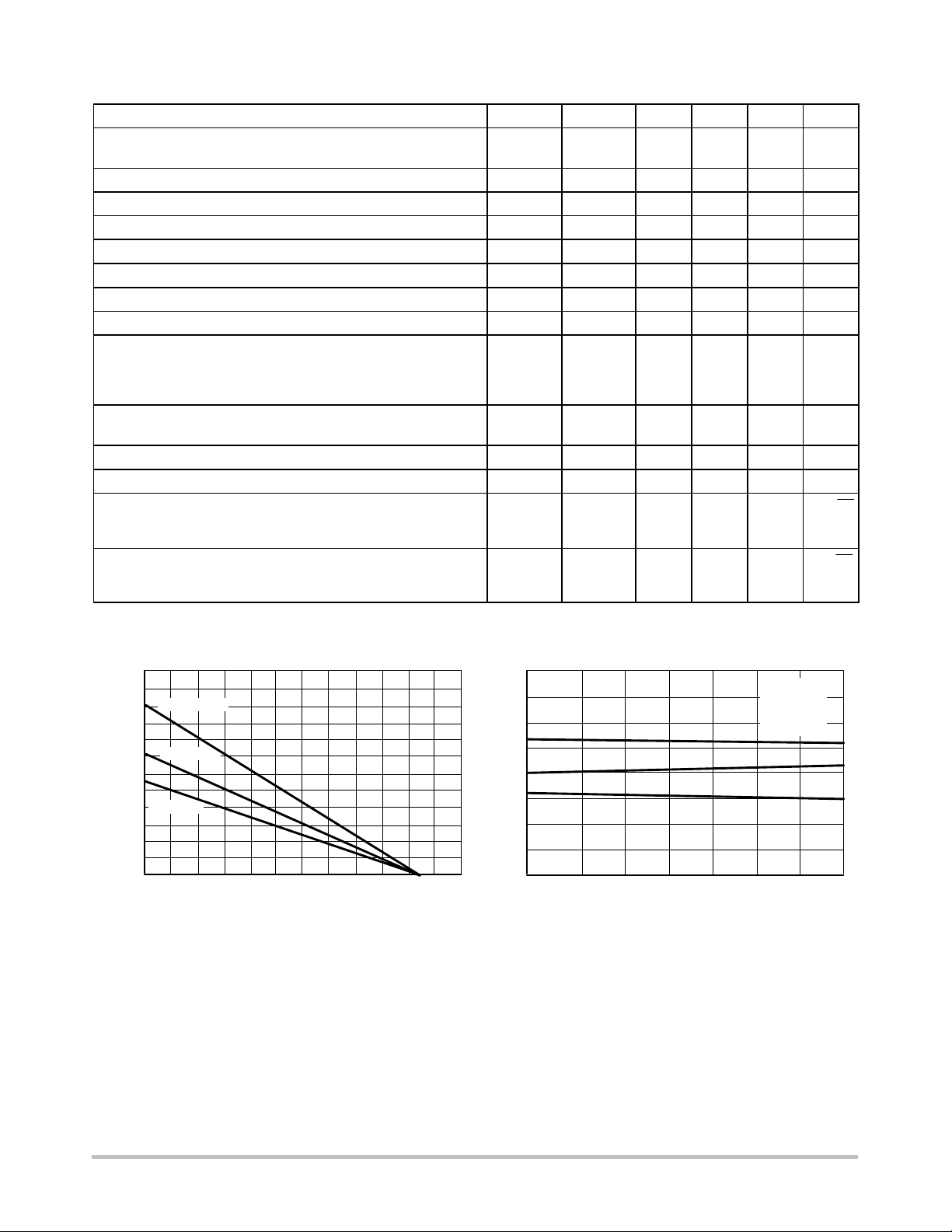
DC ELECTRICAL CHARACTERISTICS (V
Characteristics
Input Offset Voltage (RS = 50 W, VCM = 0 V, VO = 0 V)
= +15 V, VEE = −15 V, TA = 25°C, unless otherwise noted.)
CC
Figure Symbol Min Typ Max Unit
3 |VIO|
(VCC = +2.5 V, VEE = −2.5 V to VCC = +15 V, VEE = −15 V)
TA = +25°C
T
= −40° to +85°C
A
Average Temperature Coefficient of Input Offset Voltage
−
−
3
DVIO/DT
0.15
−
3.0
4.0
(RS = 50 W, VCM = 0 V, VO = 0 V)
TA = −40° to +85°C
Input Bias Current (VCM = 0 V, VO = 0 V)
TA = +25°C
TA = −40° to +85°C
Input Offset Current (VCM = 0 V, VO = 0 V)
TA = +25°C
TA = −40° to +85°C
Common Mode Input Voltage Range
(DVIO = 5.0 mV, VO = 0 V)
Large Signal Voltage Gain (VO = −10 V to +10 V, RL = 600 W)
TA = +25°C
TA = −40° to +85°C
Output Voltage Swing (VID = ±1.0 V)
4, 5 I
6 V
7, 8 A
9, 10, 11
IB
|IIO|
ICR
VOL
− 2.0 −
−
−
−
−
−13
−
50
25
100
−
5.0
−
−14
+14
200
−
500
600
50
60
−
+13
−
−
(VCC = +15 V, VEE = −15 V)
RL = 300 W
RL = 300 W
RL = 600 W
RL = 600 W
RL = 2.0 kW
RL = 2.0 kW
VO+
VO−
VO+
VO−
VO+
VO−
−
−
+12
−
+13
−
+12
−12
+13.6
−13
+14
−13.8
−
−
−
−12
−
−13
(VCC = +2.5 V, VEE = −2.5 V)
RL = 600 W
RL = 600 W
VO+
VO−
1.1
−
1.6
−1.6
−
−1.1
Common Mode Rejection (Vin = ±13 V) 12 CMR 80 110 − dB
Power Supply Rejection
VCC/VEE = +15 V/ −15 V, +5.0 V/ −15 V, +15 V/ −5.0 V
Output Short Circuit Current (VID = ±1.0 V, Output to Ground)
Source (VCC = 2.5 V to 15 V)
Sink (VEE = −2.5 V to −15 V)
Power Supply Current (VO = 0 V)
13 PSR
14, 15 I
16 I
SC
80 110 −
+50
−50
D
+80
−100
−
−
(VCC = 2.5 V, VEE = −2.5 V to VCC = +15 V, VEE = −15 V)
MC33178 (Dual)
TA = +25°C
TA = −40° to +85°C
−
−
−
−
1.4
1.6
MC33179 (Quad)
TA = +25°C
TA = −40° to +85°C
−
−
1.7
−
2.4
2.6
mV
mV/°C
nA
nA
V
kV/V
V
dB
mA
mA
http://onsemi.com
4
Page 5
MC33178, MC33179
AC ELECTRICAL CHARACTERISTICS (V
Characteristics
Slew Rate
(Vin = −10 V to +10 V, RL = 2.0 kW, CL = 100 pF, AV = +1.0 V)
= +15 V, VEE = −15 V, TA = 25°C, unless otherwise noted.)
CC
Figure Symbol Min Typ Max Unit
17, 32 SR
1.2 2.0 −
V/ms
Gain Bandwidth Product (f = 100 kHz) 18 GBW 2.5 5.0 − MHz
AC Voltage Gain (RL = 600 W, VO = 0 V, f = 20 kHz)
Unity Gain Bandwidth (Open−Loop) (RL = 600 W, CL = 0 pF)
Gain Margin (RL = 600 W, CL = 0 pF)
Phase Margin (RL = 600 W, CL = 0 pF)
19, 20 A
21, 23, 24 A
22, 23, 24
VO
BW − 3.0 − MHz
m
f
m
− 50 − dB
− 15 − dB
− 60 − Deg
Channel Separation (f = 100 Hz to 20 kHz) 25 CS − −120 − dB
Power Bandwidth (VO = 20 V
= 600 W, THD ≤ 1.0%)
pp, RL
Total Harmonic Distortion (RL = 600 W,, VO = 2.0 Vpp, AV = +1.0 V)
26 THD
BW
(f = 1.0 kHz)
(f = 10 kHz)
(f = 20 kHz)
Open Loop Output Impedance
27 |ZO|
(VO = 0 V, f = 3.0 MHz, AV = 10 V)
Differential Input Resistance (VCM = 0 V) R
Differential Input Capacitance (VCM = 0 V) C
Equivalent Input Noise Voltage (RS = 100 W,)
28 e
f = 10 Hz
f = 1.0 kHz
Equivalent Input Noise Current
29 i
f = 10 Hz
f = 1.0 kHz
p
in
in
n
n
− 32 − kHz
−
0.0024
−
0.014
−
0.024
−
−
−
− 150 −
− 200 −
− 10 − pF
nV/ Hz√
−
−
8.0
7.5
−
−
pA/ Hz√
−
−
0.33
0.15
−
−
%
W
kW
2400
2000
MC33178P/9P
1600
MC33179D
1200
800
MC33178D
400
D
0
P(MAX), MAXIMUM POWER DISSIPATION (mW)
−60 −40 −20 0 20 40 60 80 100 120 180160140
TA, AMBIENT TEMPERATURE (°C)
Figure 2. Maximum Power Dissipation
versus Temperature
4.0
3.0
2.0
Unit 1
VCC = +15 V
VEE = −15 V
RS = 10 W
VCM = 0 V
1.0
0
Unit 2
Unit 3
−1.0
−2.0
−3.0
IO
V, INPUT OFFSET VOLTAGE (mV)
−4.0
−55 −25 0 25 50 75 100 125
TA, AMBIENT TEMPERATURE (°C)
Figure 3. Input Offset Voltage versus
Temperature for 3 Typical Units
http://onsemi.com
5
Page 6

MC33178, MC33179
5
160
140
120
100
80
VCC = +15 V
60
VEE = −15 V
40
IB
I, INPUT BIAS CURRENT (nA)
TA = 25°C
20
0
−15 −10 −5.0 0 5.0 10 15
VCM, COMMON MODE VOLTAGE (V)
Figure 4. Input Bias Current
versus Common Mode Voltage
V
CC
VCC −0.5 V
VCC −1.0 V
VCC −1.5 V
VCC −2.0 V
VEE +1.0 V
VEE +0.5 V
, INPUT COMMON MODE VOLTAGE RANGE (V)
V
V
ICR
EE
−55 −25 0 25 50 75 100 125
TA, AMBIENT TEMPERATURE (°C)
VCC = +5.0 V to +18 V
VEE = −5.0 V to −18 V
DVIO = 5.0 mV
Figure 6. Input Common Mode Voltage
Range versus Temperature
120
VCC = +15 V
110
VEE = −15 V
VCM = 0 V
100
90
80
IB
70
I, INPUT BIAS CURRENT (nA)
60
−55 −25 0 25 50 75 100 125
TA, AMBIENT TEMPERATURE (°C)
Figure 5. Input Bias Current
versus Temperature
250
200
150
VCC = +15 V
100
VEE = −15 V
f = 10 Hz
DVO = 10 V to +10 V
50
, OPEN LOOP VOLTAGE GAIN (kV/V)
VOL
A
RL = 600 W
0
−55 −25 0 25 50 75 100 12
TA, AMBIENT TEMPERATURE (°C)
Figure 7. Open Loop Voltage Gain
versus Temperature
50
40
30
20
10
0
−10
−20
1A) Phase (RL = 600 W)
−30
2A) Phase (RL = 600 W, CL = 300 pF)
VOL
1B) Gain (RL = 600 W)
−40
A , OPEN LOOP VOLTAGE GAIN (dB)
2B) Gain (RL = 600 W, CL = 300 pF)
−50
2 345678910 20
f, FREQUENCY (Hz)
VCC = +15 V
VEE = −15 V
VO = 0 V
TA = 25°C
1A
1B
2B
2A
Figure 8. Voltage Gain and Phase
versus Frequency
80
100
120
140
160
180
200
220
240
260
280
φ
40
35
pp
30
25
20
15
10
, OUTPUT VOLTAGE (V )
, EXCESS PHASE (DEGREES)
O
V
5.0
0
http://onsemi.com
6
TA = 25°C
RL = 10 kW
RL = 600 W
0 5.0 10 15 20
VCC, |V
SUPPLY VOLTAGE (V)
EE|,
Figure 9. Output Voltage Swing
versus Supply Voltage
Page 7

VCC −1.0 V
VCC −2.0 V
VEE +2.0 V
VEE +1.0 V
, OUTPUT SATURATION VOLTAGE (V)
sat
V
MC33178, MC33179
V
CC
TA = +125°C
TA = −55°C
Sink
TA = −55°C
TA = +125°C
V
EE
0 5.0 10 15 20
IL, LOAD CURRENT (±mA)
Figure 10. Output Saturation Voltage
versus Load Current
Source
VCC = +5.0 V to +18 V
VEE = −5.0 V to −18 V
28
24
pp
20
16
VCC = +15 V
12
VEE = −15 V
8.0
, OUTPUT VOLTAGE (V )
O
4.0
V
RL = 600 W
AV = +1.0 V
THD = ≤1.0%
TA = 25°C
0
1.0 k 10 k 100 k 1.0 M
f, FREQUENCY (Hz)
Figure 11. Output Voltage
versus Frequency
120
100
VCC = +15 V
VEE = −15 V
VCM = 0 V
80
DVCM = ±1.5 V
TA = −55° to +125°C
60
−
A
DV
40
CM
20
CMR = 20 Log
CMR, COMMON MODE REJECTION (dB)
0
DM
+
DV
DV
DV
O
CM
x A
DM
O
10 100 1.0 k 10 k 100 k 1.0 M
f, FREQUENCY (Hz)
Figure 12. Common Mode Rejection
versus Frequency Over Temperature
100
Source
80
Sink
60
40
20
VCC = +15 V
VEE = −15 V
VID = ±1.0 V
120
TA = −55° to +125°C
100
+PSR
VCC = +15 V
VEE = −15 V
DVCC = ±1.5 V
PSR, POWER SUPPLY REJECTION (dB)
80
60
40
20
0
−
A
DM
+
PSR = 20 Log
V
CC
V
EE
DVO/A
DV
DV
−PSR
O
DM
CC
10 100 1.0 k 10 k 100 k 1.0 M
f, FREQUENCY (Hz)
Figure 13. Power Supply Rejection
versus Frequency Over Temperature
100
90
Sink
80
Source
70
60
VCC = +15 V
VEE = −15 V
VID = ±1.0 V
RL < 10 W
0
SC
I, OUTPUT SHORT CIRCUIT CURRENT (mA)
−15 −9.0 −3.0 0 3.0 9.0 15
VO, OUTPUT VOLTAGE (V)
Figure 14. Output Short Circuit Current
versus Output Voltage
50
SC
I, OUTPUT SHORT CIRCUIT CURRENT (mA)
−55 −25 0 25 50 75 100 125
http://onsemi.com
7
TA, AMBIENT TEMPERATURE (°C)
Figure 15. Output Short Circuit Current
versus Temperature
Page 8

MC33178, MC33179
O
G
G
625
μ
500
375
250
TA = +125°C
TA = +25°C
TA = −55°C
125
CC
I , SUPPLY CURRENT/AMPLIFIER ( A)
0
0 2.0 4.0 6.0 8.0 10 12 14 16 18
V
|VEE| , SUPPLY VOLTAGE (V)
CC,
Figure 16. Supply Current versus Supply
Voltage with No Load
10
8.0
6.0
4.0
VCC = +15 V
VEE = −15 V
f = 100 kHz
2.0
GBW, GAIN BANDWIDTH PRODUCT (MHz)
0
RL = 600 W
CL = 0 pF
−55 −25 0 25 50 75 100 125
TA, AMBIENT TEMPERATURE (°C)
Figure 18. Gain Bandwidth Product
versus Temperature
1.15
1.10
VCC = +15 V
VEE = −15 V
1.05
DV
= 20 V
in
pp
1.00
0.95
0.90
0.85
SR, SLEW RATE (NORMALIZED)
0.80
0.75
−55 −25 0 25 50 75 100 125
DV
−
+
in
600 W
TA, AMBIENT TEMPERATURE (°C)
Figure 17. Normalized Slew Rate
versus Temperature
50
40
30
Phase
20
10
Gain
0
−10
−20
V
A , VOLTAGE GAIN (dB)
−30
VCC = +15 V
VEE = −15 V
RL = 600 W
TA = 25°C
CL = 0 pF
−40
−50
100 k
1.0 M 10 M 100 M
f, FREQUENCY (Hz)
Figure 19. Voltage Gain and Phase
versus Frequency
V
O
100 pF
80
100
120
140
160
180
200
220
240
, EXCESS PHASE (DEGREES)
φ
260
280
50
40
30
20
AIN (dB)
10
E
0
LTA
−10
−20
1A) Phase VCC =18 V, VEE = −18 V
V
A, V
2A) Phase VCC 1.5 V, VEE = −1.5 V
−30
1B) Gain VCC = 18 V, VEE = −18 V
−40
2B) Gain VCC = 1.5 V, VEE = −1.5 V
−50
100 k
Figure 20. Voltage Gain and Phase
1B
2B
1.0 M 10 M 100 M
f, FREQUENCY (Hz)
versus Frequency
1A
2A
TA = 25°C
RL = ∞
CL = 0 pF
80
100
120
140
160
180
200
, PHASE (DEGREES)
220
φ
240
260
280
15
CL = 10 pF
12
C
= 100 pF
L
9.0
CL = 300 pF
6.0
VCC = +15 V
VEE = −15 V
3.0
RL = 600 W
m
A , OPEN LOOP GAIN MARGIN (dB)
0
−55 −25 0 25 50 75 100 125
TA, AMBIENT TEMPERATURE (°C)
Figure 21. Open Loop Gain Margin
versus Temperature
http://onsemi.com
8
Page 9

MC33178, MC33179
60
50
40
30
20
, PHASE MARGIN (DEGREES)
m
10
φ
0
−55 −25 0 25 50 75 100 125
VCC = +15 V
VEE = −15 V
RL = 600 W
CL = 10 pF
C
= 100 pF
L
CL = 300 pF
TA, AMBIENT TEMPERATURE (°C)
Figure 22. Phase Margin
versus Temperature
18
15
Phase Margin
VCC = +15 V
VEE = −15 V
VO = 0 V
12
Gain Margin
9.0
6.0
3.0
m
A, OPEN LOOP GAIN MARGIN (dB)
0
10 100 1.0 k
−
V
in
+
600 W
V
O
C
L
CL, OUTPUT LOAD CAPACITANCE (pF)
Figure 24. Open Loop Gain Margin and Phase
Margin versus Output Load Capacitance
12
10
V
CC
VEE = −15 V
8.0
R
T
VO = 0 V
6.0
TA = 25°C
4.0
m
A, GAIN MARGIN (dB)
V
2.0
in
0
100 1.0 k 10 k 100 k
60
50
150
140
40
130
30
20
10
φ
0
120
, PHASE MARGIN (DEGREES)
110
m
CS, CHANNEL SEPARATION (dB)
100
100 1.0 k 10 k 100 k 1.0 M
= +15 V
= R1+R
R
R
2
1
−
+
2
V
O
Gain Margin
Phase Margin
RT, DIFFERENTIAL SOURCE RESISTANCE (W)
Figure 23. Phase Margin and Gain Margin
versus Differential Source Resistance
Drive Channel
VCC = +15 V
CEE = −15 V
RL = 600 W
TA = 25°C
f, FREQUENCY (Hz)
Figure 25. Channel Separation
versus Frequency
60
50
40
30
20
, PHASE MARGIN (DEGREES)
m
10
φ
0
10
VCC = +15 V V
VEE = −15 V TA = 25°C
RL = 600 W
= 2.0 V
O
pp
AV = 1000
1.0
AV = 100
0.1
AV = 10
THD, TOTAL HARMONIC DISTORTION (%)
0.01
10 100 1.0 k 10 k 100 k
AV = 1.0
f, FREQUENCY (Hz)
Figure 26. Total Harmonic Distortion
versus Frequency
500
Ω
400
300
200
O
100
|Z|, OUTPUT IMPEDANCE ()
0
http://onsemi.com
9
1. AV = 1.0
2. AV = 10
3. AV = 100
4. AV = 1000
3
21
VCC = +15 V
VEE = −15 V
VO = 0 V
TA = 25°C
4
1.0 k 10 k 100 k 1.0 M 10 M
f, FREQUENCY (Hz)
Figure 27. Output Impedance
versus Frequency
Page 10

MC33178, MC33179
20
18
nV/ Hz√
16
14
Input Noise Voltage Test
+
−
12
10
8.0
6.0
4.0
2.0
n
e, INPUT REFERRED NOISE VOLTAGE ()
VCC = +15 V
VEE = −15 V
TA = 25°C
0
10 100 1.0 k 10 k 10 k
f, FREQUENCY (Hz)
Figure 28. Input Referred Noise Voltage
versus Frequency
100
90
VCC = +15 V
VEE = −15 V
80
TA = 25°C
70
60
R
50
40
= 600 W
L
RL = 2.0 kW
30
20
PERCENT OVERSHOOT (%)
10
0
10 100 1.0 k 10 k
CL, LOAD CAPACITANCE (pF)
Figure 30. Percent Overshoot versus
Load Capacitance
Circuit
0.5
pA/ Hz√
V
O
0.4
Input Noise Current Test Circuit
+
R
S
−
V
O
0.3
0.2
0.1
VCC = +15 V
VEE = −15 V
(RS = 10 kW)
TA = 25°C
0
10 100 1.0 k 10 k 100 k
n
i, INPUT REFERRED NOISE CURRENT ()
f, FREQUENCY (Hz)
Figure 29. Input Referred Noise Current
versus Frequency
VCC = +15 V
VEE = −15 V
AV = +1.0
RL = 600 W
CL = 100 pF
TA = 25°C
, OUTPUT VOLTAGE (5.0 V/DIV)
O
t, TIME (2.0 ms/DIV)
Figure 31. Non−inverting Amplifier Slew Rate
VCC = +15 V
VEE = −15 V
AV = +1.0
RL = 600 W
CL = 100 pF
TA = 25°C
, OUTPUT VOLTAGE (50 mV/DIV)
O
V
t, TIME (2.0 ns/DIV)
VCC = +15 V
VEE = −15 V
AV = +1.0
RL = 600 W
CL = 100 pF
TA = 25°C
, OUTPUT VOLTAGE (5.0 V/DIV) V
O
V
t, TIME (5.0 ms/DIV)
Figure 32. Small Signal Transient Response Figure 33. Large Signal Transient Response
http://onsemi.com
10
Page 11

10 k
MC33178, MC33179
To
Receiver
From
Microphone
120 k
2.0 k A2
−
+
V
R
A1
−
+
10 k
1.0 mF
200 k
820
−
+
0.05 mF
10 k
A3
300
10 k
V
R
Figure 34. Telephone Line Interface Circuit
10 k
1N4678
Tip
Phone Line
Ring
APPLICATION INFORMATION
This unique device uses a boosted output stage to combine
a high output current with a drain current lower than similar
bipolar input op amps. Its 60° phase margin and 15 dB gain
margin ensure stability with up to 1000 pF of load
capacitance (see Figure 24). The ability to drive a minimum
600 W load makes it particularly suitable for telecom
applications. Note that in the sample circuit in Figure 34
both A2 and A3 are driving equivalent loads of
approximately 600 W.
The low input offset voltage and moderately high slew
rate and gain bandwidth product make it attractive for a
variety of other applications. For example, although it i s not
single supply (the common mode input range does not
include ground), it is specified at +5.0 V with a typical
common mode rejection of 110 dB. This makes it an
excellent choice for use with digital circuits. The high
common mode rejection, which is stable over temperature,
coupled with a low noise figure and low distortion, is an
ideal op amp for audio circuits.
The output stage of the op amp is current limited and
therefore has a certain amount of protection in the event of
a short circuit. However, because of its high current output,
it is especially important not to allow the device to exceed
the maximum junction temperature, particularly with the
MC33179 (quad op amp). Shorting more than one amplifier
could easily exceed the junction temperature to the extent of
causing permanent damage.
Stability
As usual with most high frequency amplifiers, proper lead
dress, component placement, and PC board layout should be
exercised for optimum frequency performance. For
example, long unshielded input or output leads may result in
unwanted input/output coupling. In order to preserve the
relatively low input capacitance associated with these
amplifiers, resistors connected to the inputs should be
immediately adjacent to the input pin to minimize additional
stray input capacitance. This not only minimizes the input
pole frequency for optimum frequency response, but also
minimizes extraneous “pick up” at this node. Supplying
decoupling with adequate capacitance immediately adjacent
to the supply pin is also important, particularly over
temperature, since many types of decoupling capacitors
exhibit great impedance changes over temperature.
Additional stability problems c an be c aused b y h igh load
capacitances and/or a high source resistance. Simple
compensation schemes can be used to alleviate these
effects.
http://onsemi.com
11
Page 12

MC33178, MC33179
1)
If a high source of resistance is used (R1 > 1.0 kW), a
compensation capacitor equal to or greater than the input
capacitance of the op amp (10 pF) placed across the
feedback resistor (see Figure 35) can be used to neutralize
that pole and prevent outer loop oscillation. Since the closed
loop transient response will be a function of that
capacitance, it is important to choose the optimum value for
that capacitor. This can be determined by the following
Equation:
CC+ (1) [R1ńR2])2 CL(ZOńR2)
(
where: ZO is the output impedance of the op amp.
R2
C
C
−
R1
+
Z
L
For moderately high capacitive loads (500 pF < C
< 1500 pF) the addition of a compensation resistor on the
order of 2 0 W between the output and the feedback loop will
help to decrease miller loop oscillation (see Figure 36). For
high capacitive loads (CL > 1500 pF), a combined
compensation scheme should be used (see Figure 37). Both
the compensation resistor and the compensation capacitor
affect the transient response and can be calculated for
optimum performance. The value of CC can be calculated
using Equation 1. The Equation to calculate RC is as follows:
(2)
C
L
R1
RC+ ZO R1ńR2
R2
−
+
R
C
L
Figure 35. Compensation for
High Source Impedance
R1
Figure 36. Compensation Circuit for
R2
C
C
−
+
R
C
Figure 37. Compensation Circuit for
High Capacitive Loads
Moderate Capacitive Loads
C
L
http://onsemi.com
12
Page 13

NOTE 2
−T−
SEATING
PLANE
H
58
−B−
14
F
−A−
C
N
D
G
0.13 (0.005) B
MC33178, MC33179
PACKAGE DIMENSIONS
PDIP−8
P SUFFIX
CASE 626−05
ISSUE L
NOTES:
1. DIMENSION L TO CENTER OF LEAD WHEN
FORMED PARALLEL.
2. PACKAGE CONTOUR OPTIONAL (ROUND OR
SQUARE CORNERS).
3. DIMENSIONING AND TOLERANCING PER ANSI
Y14.5M, 1982.
DIM MIN MAX MIN MAX
A 9.40 10.16 0.370 0.400
B 6.10 6.60 0.240 0.260
C 3.94 4.45 0.155 0.175
D 0.38 0.51 0.015 0.020
L
J
K
M
M
A
T
M
M
F 1.02 1.78 0.040 0.070
G 2.54 BSC 0.100 BSC
H 0.76 1.27 0.030 0.050
J 0.20 0.30 0.008 0.012
K 2.92 3.43 0.115 0.135
L 7.62 BSC 0.300 BSC
M −−− 10 −−− 10
N 0.76 1.01 0.030 0.040
INCHESMILLIMETERS
__
SEATING
PLANE
−T−
0.038 (0.0015)
PIN 1 ID
Micro8
DM SUFFIX
CASE 846A−02
ISSUE F
−A−
K
G
−B−
D
8 PL
0.08 (0.003) A
M
T
S
B
S
C
H
J
L
NOTES:
1. DIMENSIONING AND TOLERANCING PER ANSI
Y14.5M, 1982.
2. CONTROLLING DIMENSION: MILLIMETER.
3. DIMENSION A DOES NOT INCLUDE MOLD FLASH,
PROTRUSIONS OR GATE BURRS. MOLD FLASH,
PROTRUSIONS OR GATE BURRS SHALL NOT
EXCEED 0.15 (0.006) PER SIDE.
4. DIMENSION B DOES NOT INCLUDE INTERLEAD
FLASH OR PROTRUSION. INTERLEAD FLASH OR
PROTRUSION SHALL NOT EXCEED 0.25 (0.010)
PER SIDE.
5. 846A−01 OBSOLETE, NEW STANDARD 846A−02.
DIM MIN MAX MIN MAX
A 2.90 3.10 0.114 0.122
B 2.90 3.10 0.114 0.122
C −−− 1.10 −−− 0.043
D 0.25 0.40 0.010 0.016
G 0.65 BSC 0.026 BSC
H 0.05 0.15 0.002 0.006
J 0.13 0.23 0.005 0.009
K 4.75 5.05 0.187 0.199
L 0.40 0.70 0.016 0.028
INCHESMILLIMETERS
http://onsemi.com
13
Page 14
−Y−
−Z−
MC33178, MC33179
SOIC−8
D SUFFIX
CASE 751−07
ISSUE AE
NOTES:
−X−
A
58
B
1
S
0.25 (0.010)
4
M
M
Y
K
G
N
C
SEATING
PLANE
0.10 (0.004)
H
D
0.25 (0.010) Z
M
Y
SXS
X 45
_
M
J
1. DIMENSIONING AND TOLERANCING PER
ANSI Y14.5M, 1982.
2. CONTROLLING DIMENSION: MILLIMETER.
3. DIMENSION A AND B DO NOT INCLUDE
MOLD PROTRUSION.
4. MAXIMUM MOLD PROTRUSION 0.15 (0.006)
PER SIDE.
5. DIMENSION D DOES NOT INCLUDE DAMBAR
PROTRUSION. ALLOWABLE DAMBAR
PROTRUSION SHALL BE 0.127 (0.005) TOTAL
IN EXCESS OF THE D DIMENSION AT
MAXIMUM MATERIAL CONDITION.
6. 751−01 THRU 751−06 ARE OBSOLETE. NEW
STANDARD IS 751−07.
MILLIMETERS
DIMAMIN MAX MIN MAX
4.80 5.00 0.189 0.197
B 3.80 4.00 0.150 0.157
C 1.35 1.75 0.053 0.069
D 0.33 0.51 0.013 0.020
G 1.27 BSC 0.050 BSC
H 0.10 0.25 0.004 0.010
J 0.19 0.25 0.007 0.010
K 0.40 1.27 0.016 0.050
M 0 8 0 8
____
N 0.25 0.50 0.010 0.020
S 5.80 6.20 0.228 0.244
INCHES
SOLDERING FOOTPRINT*
1.52
0.060
7.0
0.275
0.6
0.024
*For additional information on our Pb−Free strategy and soldering
details, please download the ON Semiconductor Soldering and
Mounting Techniques Reference Manual, SOLDERRM/D.
4.0
0.155
1.270
0.050
SCALE 6:1
ǒ
inches
mm
Ǔ
http://onsemi.com
14
Page 15

MC33178, MC33179
PACKAGE DIMENSIONS
PDIP−14
P SUFFIX
CASE 646−06
ISSUE N
14 8
B
17
NOTES:
1. DIMENSIONING AND TOLERANCING PER ANSI
Y14.5M, 1982.
2. CONTROLLING DIMENSION: INCH.
3. DIMENSION L TO CENTER OF LEADS WHEN
FORMED PARALLEL.
4. DIMENSION B DOES NOT INCLUDE MOLD FLASH.
5. ROUNDED CORNERS OPTIONAL.
−T−
SEATING
PLANE
N
−T−
SEATING
PLANE
HG
14 8
G
A
F
−A−
−B−
71
D 14 PL
0.25 (0.010) A
M
T
K
S
B
C
D
14 PL
0.13 (0.005)
P 7 PL
0.25 (0.010) B
C
S
K
J
M
SOIC−14
D SUFFIX
CASE 751A−03
ISSUE G
M
R X 45
_
M
DIM MIN MAX MIN MAX
A 0.715 0.770 18.16 18.80
L
M
M
J
B 0.240 0.260 6.10 6.60
C 0.145 0.185 3.69 4.69
D 0.015 0.021 0.38 0.53
F 0.040 0.070 1.02 1.78
G 0.100 BSC 2.54 BSC
H 0.052 0.095 1.32 2.41
J 0.008 0.015 0.20 0.38
K 0.115 0.135 2.92 3.43
L
0.290 0.310 7.37 7.87
M −−− 10 −−− 10
N 0.015 0.039 0.38 1.01
NOTES:
1. DIMENSIONING AND TOLERANCING PER ANSI
Y14.5M, 1982.
2. CONTROLLING DIMENSION: MILLIMETER.
3. DIMENSIONS A AND B DO NOT INCLUDE
MOLD PROTRUSION.
4. MAXIMUM MOLD PROTRUSION 0.15 (0.006)
PER SIDE.
5. DIMENSION D DOES NOT INCLUDE DAMBAR
PROTRUSION. ALLOWABLE DAMBAR
PROTRUSION SHALL BE 0.127 (0.005) TOTAL
IN EXCESS OF THE D DIMENSION AT
MAXIMUM MATERIAL CONDITION.
F
DIM MIN MAX MIN MAX
A 8.55 8.75 0.337 0.344
B 3.80 4.00 0.150 0.157
C 1.35 1.75 0.054 0.068
D 0.35 0.49 0.014 0.019
F 0.40 1.25 0.016 0.049
G 1.27 BSC 0.050 BSC
J 0.19 0.25 0.008 0.009
K 0.10 0.25 0.004 0.009
M 0 7 0 7
P 5.80 6.20 0.228 0.244
R 0.25 0.50 0.010 0.019
MILLIMETERSINCHES
__
INCHESMILLIMETERS
____
http://onsemi.com
15
Page 16

MC33178, MC33179
TSSOP−14
PACKAGE DIMENSIONS
DTB SUFFIX
CASE 948G−01
ISSUE A
0.10 (0.004)
−T−
SEATING
PLANE
14X REFK
S
U
T
S
N
0.25 (0.010)
U0.15 (0.006) T
S
2X L/2
0.10 (0.004) V
14
M
8
M
L
PIN 1
IDENT.
1
S
U0.15 (0.006) T
A
−V−
B
N
−U−
F
7
DETAIL E
K
K1
J J1
SECTION N−N
C
D
G
H
DETAIL E
NOTES:
1. DIMENSIONING AND TOLERANCING PER
ANSI Y14.5M, 1982.
2. CONTROLLING DIMENSION: MILLIMETER.
3. DIMENSION A DOES NOT INCLUDE MOLD
FLASH, PROTRUSIONS OR GATE BURRS.
MOLD FLASH OR GATE BURRS SHALL NOT
EXCEED 0.15 (0.006) PER SIDE.
4. DIMENSION B DOES NOT INCLUDE
INTERLEAD FLASH OR PROTRUSION.
INTERLEAD FLASH OR PROTRUSION SHALL
NOT EXCEED 0.25 (0.010) PER SIDE.
5. DIMENSION K DOES NOT INCLUDE DAMBAR
PROTRUSION. ALLOWABLE DAMBAR
PROTRUSION SHALL BE 0.08 (0.003) TOTAL
IN EXCESS OF THE K DIMENSION AT
MAXIMUM MATERIAL CONDITION.
6. TERMINAL NUMBERS ARE SHOWN FOR
REFERENCE ONLY.
7. DIMENSION A AND B ARE TO BE
DETERMINED AT DATUM PLANE −W−.
INCHESMILLIMETERS
−W−
DIM MIN MAX MIN MAX
A 4.90 5.10 0.193 0.200
B 4.30 4.50 0.169 0.177
C −−− 1.20 −−− 0.047
D 0.05 0.15 0.002 0.006
F 0.50 0.75 0.020 0.030
G 0.65 BSC 0.026 BSC
H 0.50 0.60 0.020 0.024
J 0.09 0.20 0.004 0.008
J1 0.09 0.16 0.004 0.006
K 0.19 0.30 0.007 0.012
K1 0.19 0.25 0.007 0.010
L 6.40 BSC 0.252 BSC
M 0 8 0 8
____
ON Semiconductor and are registered trademarks of Semiconductor Components Industries, LLC (SCILLC). SCILLC reserves the right to make changes without further notice
to any products herein. SCILLC makes no warranty, representation or guarantee regarding the suitability of its products for any particular purpose, nor does SCILLC assume any liability
arising out of the application or use of any product or circuit, and specifically disclaims any and all liability, including without limitation special, consequential or incidental damages.
“Typical” parameters which may be provided in SCILLC data sheets and/or specifications can and do vary in different applications and actual performance may vary over time. All
operating parameters, including “Typicals” must be validated for each customer application by customer’s technical experts. SCILLC does not convey any license under its patent rights
nor the rights of others. SCILLC products are not designed, intended, or authorized for use as components in systems intended for surgical implant into the body, or other applications
intended to support or sustain life, or for any other application in which the failure of the SCILLC product could create a situation where personal injury or death may occur. Should
Buyer purchase or use SCILLC products for any such unintended or unauthorized application, Buyer shall indemnify and hold SCILLC and its officers, employees, subsidiaries, affiliates,
and distributors harmless against all claims, costs, damages, and expenses, and reasonable attorney fees arising out of, directly or indirectly, any claim of personal injury or death
associated with such unintended or unauthorized use, even if such claim alleges that SCILLC was negligent regarding the design or manufacture of the part. SCILLC is an Equal
Opportunity/Affirmative Action Employer. This literature is subject to all applicable copyright laws and is not for resale in any manner.
PUBLICATION ORDERING INFORMATION
LITERATURE FULFILLMENT:
Literature Distribution Center for ON Semiconductor
P.O. Box 61312, Phoenix, Arizona 85082−1312 USA
Phone: 480−829−7710 or 800−344−3860 Toll Free USA/Canada
Fax: 480−829−7709 or 800−344−3867 Toll Free USA/Canada
Email: orderlit@onsemi.com
N. American Technical Support: 800−282−9855 Toll Free
USA/Canada
Japan: ON Semiconductor, Japan Customer Focus Center
2−9−1 Kamimeguro, Meguro−ku, Tokyo, Japan 153−0051
Phone: 81−3−5773−3850
http://onsemi.com
16
ON Semiconductor Website: http://onsemi.com
Order Literature: http://www.onsemi.com/litorder
For additional information, please contact your
local Sales Representative.
MC33178/D
 Loading...