

Page 1
MC26LS30
Dual Differential
(EIA-422-A)/
Quad Single-Ended
(EIA-423-A) Line Drivers
The MC26LS30 is a low power Schottky set of line drivers which
can be configured as two differential drivers which comply with
EIA–422–A standards, or as four single–ended drivers which comply
with EIA–423–A standards. A mode select pin and appropriate choice
of power supplies determine the mode. Each driver can source and
sink currents in excess of 50 mA.
In the differential mode (EIA–422–A), the drivers can be used up to
10 Mbaud. A disable pin for each driver permits setting the outputs
into a high impedance mode within a +10 V common mode range.
In the single–ended mode (EIA–423–A), each driver has a slew rate
control pin which permits setting the slew rate of the output signal so
as to comply with EIA–423–A and FCC requirements and to reduce
crosstalk. When operated from symmetrical supplies (+5.0 V), the
outputs exhibit zero imbalance
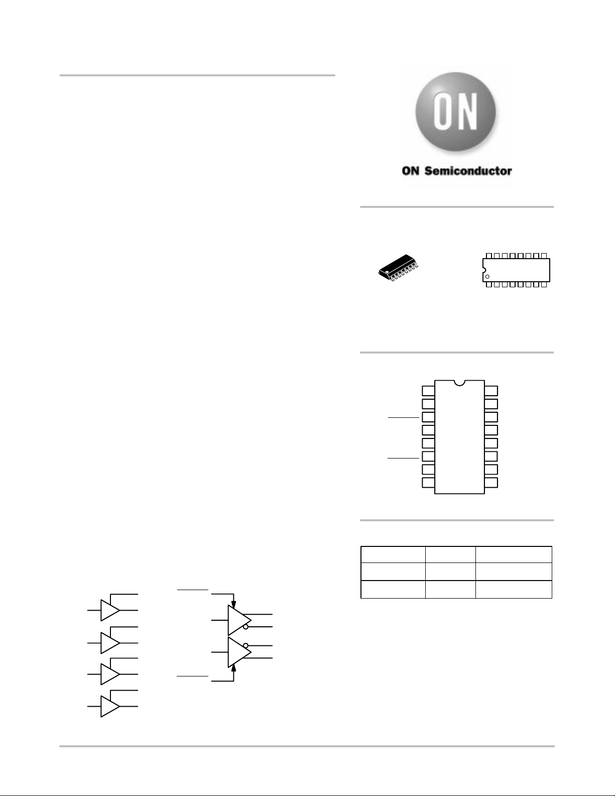
The MC26LS30 is available in a 16–pin surface mount package.
Operating temperature range is –40° to +85°C.
16
http://onsemi.com
SO–16
D SUFFIX
1
CASE 751B
A = Assembly Location
WL, L = Wafer Lot
YY, Y = Year
WW, W= Work Week
PIN CONNECTIONS
MARKING
DIAGRAM
16
MC26LS30D
AWLYWW
1
• Operates as Two Differential EIA–422–A Drivers, or Four
Single–Ended EIA–423–A Drivers
• High Impedance Outputs in Differential Mode
• Short Circuit Current Limit In Both Source and Sink Modes
• ±10 V Common Mode Range on High Impedance Outputs
• ±15 V Range on Inputs
• Low Current PNP Inputs Compatible with TTL, CMOS, and MOS
Outputs
• Individual Output Slew Rate Control in Single–Ended Mode
• Replacement for the AMD AM26LS30 and National Semiconductor
DS3691
Representative Block Diagrams
Single–Ended Mode
EIA–423–A
Input A
Input B
Input C
Input D
SR-A
Out A
SR-B
Out B
SR-C
Out C
SR-D
Out D
Differential Mode
Enable AB
Input A
Input D
Enable CD
V
CC
VEE-8
EIA–422–A
-1
Out A
Out B
Out C
Out D
Gnd-5
Mode-4
V
Input A
Input B/
Enable AB
Mode
Gnd
Input C/
Enable CD
Input D
V
1
CC
2
3
4
5
6
7
8
EE
(Top View)
16
15
14
13
12
11
10
9
ORDERING INFORMATION
Device Package Shipping
MC26LS30D 48 Units/RailSO–16
MC26LS30DR2 2500 Tape & ReelSO–16
SR-A
Output A
Output B
SR-B
SR-C
Output C
Output D
SR-D
Semiconductor Components Industries, LLC, 2000
July, 2000 – Rev. 1
1 Publication Order Number:
MC26LS30/D
Page 2
MC26LS30
MAXIMUM OPERATING CONDITIONS (Pin numbers refer to SO–16 package only.)
Rating
Power Supply Voltage V
Input Voltage (All Inputs) V
Applied Output Voltage when in High Impedance Mode
= 5.0 V, Pin 4 = Logic 0, Pins 3, 6 = Logic 1)
(V
CC
Output Voltage with VCC, VEE = 0 V V
Output Current I
Junction Temperature T
Devices should not be operated at these limits. The “Recommended Operating Conditions” table provides conditions for actual device operation.
RECOMMENDED OPERATING CONDITIONS
Rating Symbol Min Typ Max Unit
Power Supply Voltage (Differential Mode) V
Power Supply Voltage (Single–Ended Mode) V
Input Voltage (All Inputs) V
Applied Output Voltage (when in High Impedance Mode) V
Applied Output Voltage, V
= 0 V
CC
Output Current I
Operating Ambient Temperature (See text) T
All limits are not necessarily functional concurrently.
V
V
Symbol Value Unit
–0.5, +7.0
–7.0, +0.5
–0.5, +20 Vdc
±15 Vdc
±15
Self limiting –
–65, +150 °C
5.0
0
+5.0
–5.0
CC
EE
CC
EE
za
zb
O
CC
V
EE
in
V
za
zb
O
J
+4.75
–0.5
+4.75
–5.25
in
0 – +15 Vdc
–10 – +10
–10 – +10
–65 – +65 mA
A
–40 – +85 °C
+5.25
+0.3
+5.25
–4.75
Vdc
Vdc
http://onsemi.com
2
Page 3
MC26LS30
ELECTRICAL CHARACTERISTICS (EIA–422–A differential mode, Pin 4 0.8 V, –40°C T
V
= Gnd, unless otherwise noted. Pin numbers refer to SO–16 package only.)
EE
Characteristic
Output Voltage (see Figure 1)
Differential, R
Differential, R
Change in Differential Voltage, R
Offset Voltage, R
Change in Offset Voltage*, R
= ∞, VCC = 5.25 V
L
= 100 Ω, VCC = 4.75 V
L
= 100 Ω
L
L
= 100 Ω
L
= 100 Ω (Note 4.)
Output Current (each output)
Power Off Leakage, V
High Impedance Mode, V
= 0, –10 V VO +10 V
CC
= 5.25 V, –10 V VO +10 V
CC
Short Circuit Current (Note 2.)
High Output Shorted to Pin 5 (T
High Output Shorted to Pin 5 (–40°C T
Low Output Shorted to +6.0 V (T
Low Output Shorted to +6.0 V (–40°C T
= 25°C)
A
= 25°C)
A
+85°C)
A
+85°C)
A
Inputs
Low Level Voltage
High Level Voltage
Current @ V
Current @ V
Current @ V
Current, 0 V
Clamp Voltage (I
= 2.4 V
in
= 15 V
in
= 0.4 V
in
15 V, VCC = 0
in
= –12 mA)
in
Power Supply Current (VCC = +5.25 V, Outputs Open)
(0 Enable V
CC
)
Symbol Min Typ Max Unit
V
OD1
V
OD2
∆V
OD2
V
OS
∆VOS
I
OLK
I
OZ
I
SC–
I
SC–
I
SC+
I
SC+
V
IL
V
IH
I
IH
I
IHH
I
IL
I
IX
V
IK
I
CC
–
2.0
–
–
–
–100
–100
–150
–150
60
50
–
2.0
–
–
–200
–
–1.5
– 16 30
85°C, 4.75 V VCC 5.25 V,
A
4.2
2.6
10
2.5
10
0
0
–95
–
75
–
–
–
0
0
–8.0
0
–
6.0
–
400
3.0
400
+100
+100
–60
–50
150
150
0.8
–
40
100
–
–
–
Vdc
Vdc
mVdc
Vdc
mVdc
Vdc
Vdc
Vdc
µA
mA
µA
mA
TIMING CHARACTERISTICS (EIA–422–A differential mode, Pin 4 0.8 V, T
unless otherwise noted.)
Characteristic
Differential Output Rise Time (Figure 3) t
Differential Output Fall Time (Figure 3) t
Propagation Delay Time – Input to Differential Output
Input Low to High (Figure 3)
Input High to Low (Figure 3)
Skew Timing (Figure 3)
t
to t
PDH
Max to Min t
Max to Min t
Enable Timing (Figure 4)
Enable to Active High Differential Output
Enable to Active Low Differential Output
Enable to 3–State Output From Active High
Enable to 3–State Output From Active Low
1. All voltages measured with respect to Pin 5.
2. Only one output shorted at a time, for not more than 1 second.
3. Typical values established at +25°C, V
4. V
switched from 0.8 to 2.0 V.
in
5. Imbalance is the difference between V
for Each Driver
PDL
Within a Package
PDH
Within a Package
PDL
= +5.0 V, VEE = –5.0 V.
CC
with Vin 0.8 V and VO2 with Vin 2.0 V.
O2
= 25°C, VCC = 5.0 V, VEE = Gnd, (Notes 1. and 3.)
A
Symbol Min Typ Max Unit
r
f
– 70 200 ns
– 70 200 ns
ns
t
PDH
t
PDL
–
–
90
90
200
200
ns
t
SK1
t
SK2
t
SK3
–
–
–
9.0
2.0
2.0
–
–
–
ns
t
PZH
t
PZL
t
PHZ
t
PLZ
–
–
–
–
150
190
80
110
300
350
350
300
http://onsemi.com
3
Page 4
MC26LS30
ELECTRICAL CHARACTERISTICS (EIA–423–A single–ended mode, Pin 4 2.0 V, –40°C T
|V
5.25 V, (Notes 1. and 3.) unless otherwise noted).
EE
Characteristic
Output Voltage (VCC = VEE = 4.75 V)
Single–Ended Voltage, R
Single–Ended Voltage, R
Voltage Imbalance (Note 5.), R
= ∞ (Figure 2)
L
= 450 Ω, (Figure 2)
L
= 450 Ω
L
Slew Control Current (Pins 16, 13, 12, 9) I
Output Current (Each Output)
Power Off Leakage, V
= VEE = 0, –6.0 V VO +6.0 V
CC
Short Circuit Current (Output Short to Ground, Note 2.)
0.8 V (TA = 25°C)
V
in
0.8 V (–40°C TA +85°C)
V
in
V
2.0 V (TA = 25°C)
in
2.0 V (–40°C TA +85°C)
V
in
Inputs
Low Level Voltage
High Level Voltage
Current @ V
Current @ V
Current @ V
Current, 0 V
Clamp Voltage (I
= 2.4 V
in
= 15 V
in
= 0.4 V
in
15 V, VCC = 0
in
= –12 mA)
in
Power Supply Current (Outputs Open)
= +5.25 V, VEE = –5.25 V, Vin = 0.4 V
V
CC
Symbol Min Typ Max Unit
VO1
V
∆V
SLEW
I
OLK
I
SC+
I
SC+
I
SC–
I
SC–
V
V
I
I
IHH
I
I
V
I
CC
I
EE
O2
O2
IL
IH
IH
IL
IX
IK
4.0
3.6
–
– ±120 – µA
–100
60
50
–150
–150
–
2.0
–
–
–200
–
–1.5
–
–22
85°C, 4.75 V V
A
4.2
3.95
0.05
0
80
–
–95
–
–
–
0
0
–8.0
0
–
17
–8.0
6.0
6.0
0.4
+100
150
150
–60
–50
0.8
–
40
100
–
–
–
30
–
CC
,
Vdc
µA
mA
Vdc
Vdc
µA
Vdc
mA
TIMING CHARACTERISTICS (EIA–423–A single–ended mode, Pin 4 2.0 V, T
3.) unless otherwise noted.)
Characteristic
Output Timing (Figure 5)
Output Rise Time, C
Output Fall Time, C
Output Rise Time, C
Output Fall Time, C
Rise Time Coefficient (Figure 16) C
Propagation Delay Time, Input to Single Ended Output (Figure 5)
Input Low to High, C
Input High to Low, C
Skew Timing, CC = 0 (Figure 5)
to t
t
PDH
Max to Min t
Max to Min t
for Each Driver
PDL
PDH
PDL
1. All voltages measured with respect to Pin 5.
2. Only one output shorted at a time, for not more than 1 second.
3. Typical values established at +25°C, V
4. V
switched from 0.8 to 2.0 V.
in
5. Imbalance is the difference between V
= 0
C
= 0
C
= 50 pF
C
= 50 pF
C
= 0
C
= 0
C
Within a Package
Within a Package
= +5.0 V, VEE = –5.0 V.
CC
with Vin 0.8 V and VO2 with Vin 2.0 V.
O2
= 25°C, VCC = 5.0 V, VEE = –5.0 V, (Notes 1. and
A
Symbol Min Typ Max Unit
t
r
t
f
t
r
t
f
rt
–
–
–
–
65
65
3.0
3.0
300
300
–
–
ns
µs
– 0.06 – µs/pF
ns
t
PDH
t
PDL
–
–
100
100
300
300
ns
t
SK4
t
SK5
t
SK6
–
–
–
15
2.0
5.0
–
–
–
http://onsemi.com
4
Page 5
Differential
+5.0
Gnd
00010000010110100
(EIA 422 A)
001X0100111Z0Z001
00X1100010Z1Z0011
00100000011001100
000100011X01100Z1
S g e ded
50
50
010000000100000
(EIA 423 A)
11100100001001000
11001001000010010
11000010010000100
V
in
(0.8 or 2.0 V)
Mode = 0
MC26LS30
T able 1
Inputs Outputs
Operation V
CC
Differential +5.0 Gnd 0 0 0 0 0 0 1 1 0
(EIA–422–A)
Single–Ended +5.0 –5.0 1 0 0 0 0 0 0 0 0
(EIA–423–A)
X 0 X X X X X X Z Z Z Z
X = Don’t Care
Z = High Impedance (Off)
V
CC
/2
R
L
V
OD2
RL/2
V
Mode A B C D A B C D
EE
1
V
CC
V
in
(0.8 or 2.0 V)
V
OS
Mode = 1
V
EE
1
1
0
1
Z
0
0
0
1
R
C
L
L
V
O
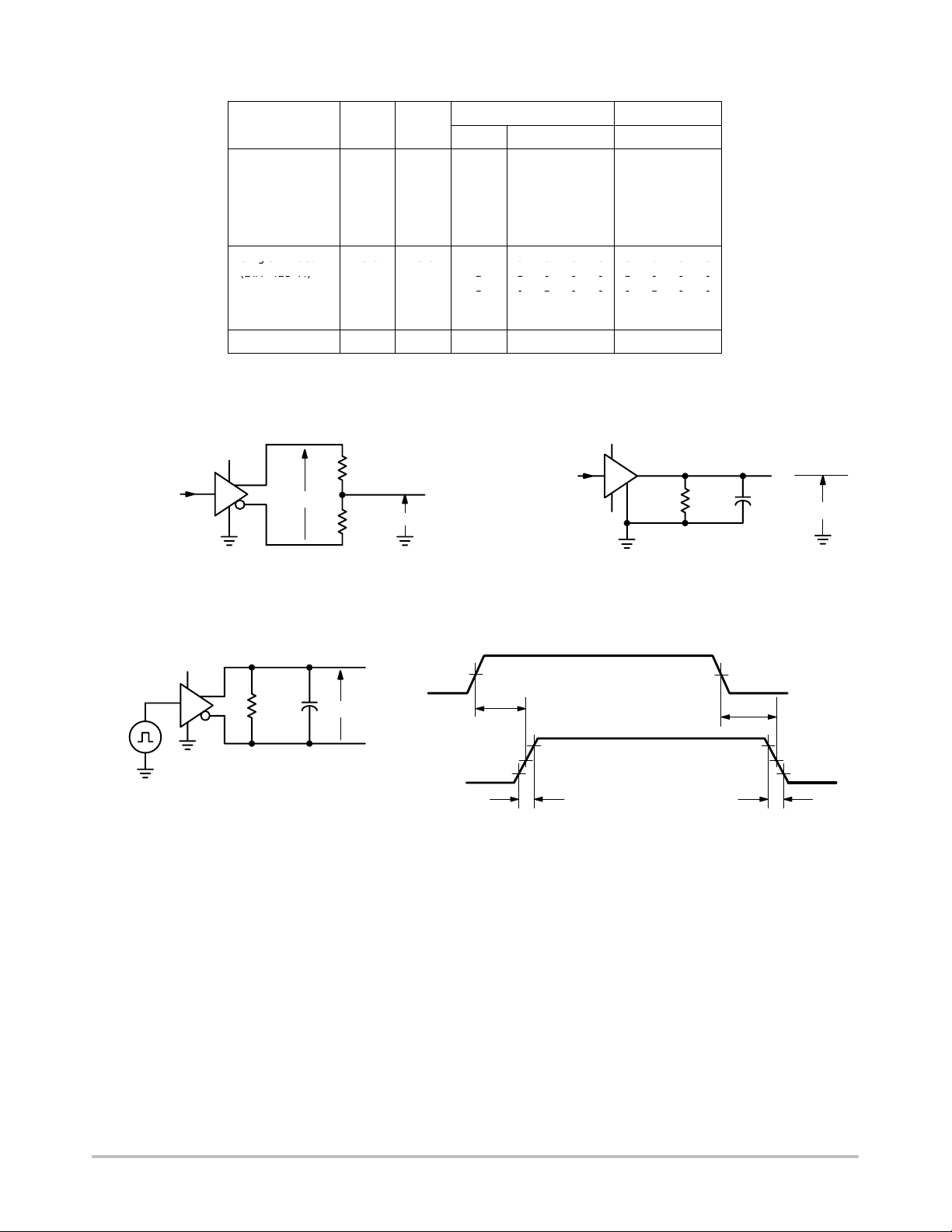
Figure 1. Differential Output Test Figure 2. Single–Ended Output Test
V
CC
V
in
100
500 pF
V
OD
S.G.
NOTES:
1. S.G. set to: f 1.0 MHz; duty cycle = 50%; t
2. t
= t
SK1
3. t
4. t
PDH–tPDL
computed by subtracting the shortest t
SK2
computed by subtracting the shortest t
SK3
for each driver.
Figure 3. Differential Mode Rise/Fall Time and Data Propagation Delay
, tf, 10 ns.
r
from the longest t
PDH
from the longest t
PDL
+3.0 V
V
in
1.5 V
t
PDH
90%
50%
V
out
10%
t
r
of the 2 drivers within a package.
PDH
of the 2 drivers within a package.
PDL
1.5 V
t
f
t
0 V
PDL
90%
50%
10%
http://onsemi.com
5
Page 6
MC26LS30
V
CC
V
0 or 3.0 V
V
in
S.G.
En
500 pF
450 Ω
R
L
V
SS
in
(Vin = Hi)
Output
Current
= Lo)
(V
in
NOTES:
1. S.G. set to: f 1.0 MHz; duty cycle = 50%; t
, tf, 10 ns.
r
2. Above tests conducted by monitoring output current levels.
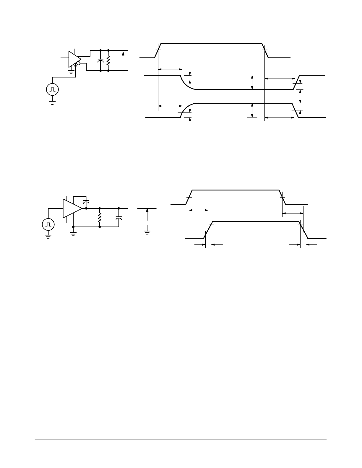
Figure 4. Differential Mode Enable Timing
V
CC
C
Vin
V
EE
S.G.
NOTES:
1. S.G. set to: f 100 kHz; duty cycle = 50%; t
2. t
= t
SK4
3. t
4. t
PDH–tPDL
computed by subtracting the shortest t
SK5
computed by subtracting the shortest t
SK6
C
450
for each driver.
500 pF
, tf, 10 ns.
r
PDH
PDL
V
O
from the longest t
from the longest t
1.5 V
t
t
PHZ
PLZ
0.1 VSS/R
L
0.1 V
SS/RL
V
in
1.5 V
t
PDH
90%
50%
V
out
10%
of the 4 drivers within a package.
PDH
of the 4 drivers within a package.
PDL
+3.0 V
1.5 V
0 V
t
PZH
VSS/R
VSS/R
L
L
t
PZL
0.5 VSS/R
0.5 VSS/R
L
L
+2.5 V
1.5 V
0 V
t
PDL
90%
50%
10%
t
r
t
f
Figure 5. Single–Ended Mode Rise/Fall Time and Data Propagation Delay
http://onsemi.com
6
Page 7

MC26LS30
5.0
4.0
3.0
2.0
, OUTPUT VOLTAGE (V)
OD
V
1.0
0
+100
+60
+20
-20
-60
, SHORT CIRCUIT CURRENT (mA)
SC
I
-100
Differential Mode
Mode = 0, VCC = 5.0 V
0.8 or
2.0 V
I
O
V
OD
, OUTPUT CURRENT (mA)
I
O
Figure 6. Differential Output Voltage
versus Load Current
Normally Low Output
Normally High Output
Differential Mode
Mode = 0, V
1.0
Vza, APPLIED OUTPUT VOLTAGE (V)
Figure 8. Short Circuit Current
versus Output Voltage
CC
= 5.0 V
40
Differential Mode
Mode = 0
Supply Current = Bias Current + Load Current
30
20
, BIAS CURRENT (mA)
B
VCC = 5.25 V
I
6050403020100
10
20
TOTAL LOAD CURRENT (mA)
1201008060040
Figure 7. Internal Bias Current
versus Load Current
+5.0
VCC = 0
0
-5.0
-10
-15
INPUT CURRENT A)
in
I
-20
6.05.04.03.02.00
-25
VCC = 5.0 V
Pins 2 to 4, 6, 7
-5.0 V VEE 0
Differential or
Single-Ended Mode
, INPUT VOLTAGE (V)
V
in
(Pin numbers refer to SO–16 package only.)
1513119.07.05.03.01.0-1.0
Figure 9. Input Current versus Input Voltage
4.5
4.0
3.5
, OUTPUT VOLTAGE (V)
OH
V
3.0
Single-Ended Mode
Mode = 1
VCC = 5.0 V, VEE = -5.0 V
Vin = 1
0
Figure 10. Output Voltage versus
I
, OUTPUT CURRENT (mA)
OH
Output Source Current
-3.25
-3.75
-4.25
, OUTPUT VOLTAGE (V)
OL
V
-4.75
-60-40-30 -50-20-10
0
http://onsemi.com
7
Single-Ended Mode
Mode = 1
VCC = 5.0 V, VEE = -5.0 V
Vin = 0
2010
I
, OUTPUT CURRENT (mA)
OL
Figure 11. Output Voltage versus
Output Sink Current
60504030
Page 8

MC26LS30
26
22
18
, BIAS CURRENT (mA)
B+
14
I
10
100
-20
-60
, SHORT CIRCUIT CURRENT (mA)
SC
I
-100
Single Ended Mode
Mode = 1
V
= 5.0 V, VEE = -5.0 V
CC
Supply Current = Bias Current + I
OH
Vin = LoVin = Hi
-80
I
OL
TOTAL LOAD CURRENT (mA)
Figure 12. Internal Positive Bias Current
versus Load Current
60
20
Single-Ended Mode
Mode = 1
VCC = 5.0 V, VEE = -5.0 V
Normally Low Output
Normally High Output
-2.0-4.0-6.0 2.0 4.0 6.0
V
, APPLIED OUTPUT VOLTAGE (V)
za
0
0
-5.0
-10
Vin = LoV
= Hi
in
, BIAS CURRENT (mA)
B-
-15
I
Single-Ended Mode
Mode = 1
VCC = 5.0 V, VEE = -5.0 V
Supply Current = Bias Current + I
I
-2400 -160240 160 80
OH
-20
I
OL
OL
-80 -2400 -160240 160 80
I
OH
TOTAL LOAD CURRENT (mA)
Figure 13. Internal Negative Bias Current
versus Load Current
110
Normally Low Output
Normally High Output to Ground
020 85
T
, AMBIENT TEMPERATURE (°C)
A
40
60-20
+ (mA)
SC
-90
- (mA) I
-100
SC
I
-110
90
70
Single or Differential Mode
VCC = 5.0 V, VEE = -5.0 V or Gnd
50
-40
Figure 14. Short Circuit Current
versus Output Voltage
1.0 k
Single-Ended Mode
Mode = 1
µ, t
VCC = 5.0 V, VEE = -5.0 V
100
, RISE/FALL TIME ( s)t
10
f
r
1.0
10
Figure 16. Rise/Fall Time versus Capacitance
100
C
, CAPACITANCE (pF)
C
http://onsemi.com
8
Figure 15. Short Circuit Current
versus
Temperature
1.0 k
10 k
Page 9

MC26LS30
APPLICATIONS INFORMATION
(Pin numbers refer to SO–16 package only.)
Description
The MC26LS30 is a dual function line driver – it can be
configured as two differential output drivers which comply
with EIA–422–A Standard, or as four single–ended drivers
which comply with EIA–423–A Standard. The mode of
operation is selected with the Mode pin (Pin 4) and
appropriate power supplies (see Table 1). Each of the four
outputs is capable of sourcing and sinking 60 to 7 0 m A while
providing sufficient voltage to ensure proper data
transmission.
As differential drivers, data rates to 10 Mbaud can be
transmitted over a twisted pair for a distance determined by
the cable characteristics. EIA–422–A Standard provides
guidelines for cable length versus data rate. The advantage
of a differential (balanced) system over a single–ended
system is greater noise immunity, common mode rejection,
and higher data rates.
Where extraneous noise sources are not a problem, the
MC26LS30 may be configured as four single–ended drivers
transmitting data rates to 100 Kbaud. Crosstalk among wires
within a cable is controlled by the use of the slew rate control
pins on the MC26LS30.
Mode Selection (Differential Mode)
In this mode (Pins 4 and 8 at ground), only a +5.0 V supply
±5% is required at VCC. Pins 2 and 7 are the driver inputs,
while Pins 10, 11, 14 and 15 are the outputs (see Block
Diagram on page 1). The two outputs of a driver are always
complementary and the differential voltage available at each
pair of outputs is shown in Figure 6 for V
= 5.0 V. The
CC
differential output voltage will vary directly with VCC. A
“high” output can only source current, while a “low” output
can only sink current (except for short circuit current – see
Figure 8).
The two outputs will be in a high impedance mode when
the respective Enable input (Pin 3 or 6) is high, or if V
CC
1.1 V. Output leakage current over a common mode range of
± 10 V is typically less than 1.0 µA.
The outputs have short circuit current limiting, typically,
less than 100 mA over a voltage range of 0 to +6.0 V (see
Figure 8). Short circuits should not be allowed to last
indefinitely as the IC may be damaged.
Pins 9, 12, 13 and 16 are not normally used when in this
mode, and should be left open.
(Single–Ended Mode)
In this mode (Pin 4 ≥ 2.0 V) VCC requires +5.0 V, and V
EE
requires –5.0 V, both ±5.0%. Pins 2, 3, 6, and 7 are inputs for
the four drivers, and Pins 15, 14, 11, and 10 (respectively)
are the outputs. The four drivers are independent of each
other, and each output will be at a positive or a negative
voltage depending on its input state, the load current, and the
supply voltage. Figures 10 & 11 indicate the high and low
output voltages for V
= 5.0 V, and VEE = –5.0 V. The graph
CC
of Figure 10 will vary directly with VCC, and the graph of
Figure 11 will vary directly with VEE. A “high” output can
only source current, while a “low” output can only sink
current (except short circuit current – see Figure 14).
The outputs will be in a high impedance mode only if
V
1.1 V. Changing VEE to 0 V does not set the outputs
CC
to a high impedance mode. Leakage current over a common
mode range of ±10 V is typically less than 1.0 µA.
The outputs have short circuit current limiting, typically
less than 100 mA over a voltage range of ±6.0 V (see Figure
14). Short circuits should not be allowed to last indefinitely
as the IC may be damaged.
Capacitors connected between Pins 9, 12, 13, and 16 and
their respective outputs will provide slew rate limiting of the
output transition. Figure 16 indicates the required capacitor
value to obtain a desired rise or fall time (measured between
the 10% and 90% points). The positive and negative
transition times will be within ≈ ±5% of each other. Each
output may be set to a different slew rate if desired.
Inputs
The five inputs determine the state of the outputs in
accordance with Table 1. All inputs (regardless of the
operating mode) have a nominal threshold of +1.3 V, and
their voltage must be kept within a range of 0 V to +15 V for
proper operation. If an input is taken more than 0.3 V below
ground, excessive currents will flow, and the proper
operation of the drivers will be affected. An open pin is
equivalent to a logic high, but good design practices dictate
that inputs should never be left open. Unused inputs should
be connected to ground. The characteristics of the inputs are
shown in Figure 9.
Power Supplies
VCC requires +5.0 V, ±5%, regardless of the mode of
operation. The supply current is determined by the IC’s
internal bias requirements and the total load current. The
internally required current is a function of the load current
and is shown in Figure 7 for the differential mode.
In the single–ended mode, V
must be –5.0 V, ±5% in
EE
order to comply with EIA–423–A standards. Figures 12 and
13 indicate the internally required bias currents as a function
of total load current (the sum of the four output loads). The
discontinuity at 0 load current exists due to a change in bias
current when the inputs are switched. The supply currents
vary ≈ ± 2.0 mA as V
and VEE are varied from 4.75 V
CC
to 5.25 V.
Sequencing of the supplies during power–up/
power–down is not required.
Bypass capacitors (0.1 µF minimum on each supply pin)
are recommended to ensure proper operation. Capacitors
reduce noise induced onto the supply lines by the switching
action of the drivers, particularly where long P.C. board
tracks are involved. Additionally, the capacitors help absorb
http://onsemi.com
9
Page 10

MC26LS30
transients induced onto the drivers’ outputs from the
external cable (from ESD, motor noise, nearby computers,
etc.).
Operating Temperature Range
The maximum ambient operating temperature, listed as
+85°C, is actually a function of the system use (i.e.,
specifically how many drivers within a package are used)
and at what current levels they are operating. The maximum
power which may be dissipated within the package is
determined by:
T
T
where R
P
Dmax
= package thermal resistance which is typically:
JA
θ
Jmax
R
A
JA
120°C/W for the SOIC (D) package,
T
= max. allowable junction temperature (150°C)
Jmax
TA = ambient air temperature near the IC package.
1) Differential Mode Power Dissipation
For the differential mode, the power dissipated within the
package is calculated from:
PD [(VCC VOD) IO] (each driver) (VCC IB)
where: VCC= the supply voltage
VOD= is taken from Figure 6 for the known
value of I
I
= the internal bias current (Figure 7)
B
O
As indicated in the equation, the first term (in brackets) must
be calculated and summed for each of the two drivers, while
the last term is common to the entire package. Note that the
term (VCC –VOD) is constant for a given value of IO and does
not vary with VCC. For an application involving the
following conditions:
TA = +85°C, IO = –60 mA (each driver), VCC = 5.25 V, the
suitability of the package types is calculated as follows.
The power dissipated is:
PD [3.0V 60 mA 2] (5.25 V 18 mA)
PD 454 mW
The junction temperature calculates to:
TJ 85°C (0.454 W 120° CW) 139°C for the
SOIC package.
Since the maximum allowable junction temperature is not
exceeded in any of the above cases, either package can be
used in this application.
2) Single–Ended Mode Power Dissipation
For the single–ended mode, the power dissipated within
the package is calculated from:
P
[(
D
I
O
(
IB V
(
VCC V
CC
OH
)(
)](
IB V
each driver
EE
)
)
The above equation assumes IO has the same magnitude
for both output states, and makes use of the fact that the
absolute value of the graphs of Figures 10 and 11 are nearly
identical. IB+ and IB– are obtained from the right half of
Figures 12 and 13, and (V
Figure 10. Note that the term (V
– VOH) can be obtained from
CC
– VOH) is constant for a
CC
given value of IO and does not vary with VCC. For an
application involving the following conditions:
TA = +85°C, IO = –60 mA (each driver), VCC = 5.25 V,
V
= –5.25 V, the suitability of the package types is
EE
calculated as follows.
The power dissipated is:
(
P
24 mA 5.25 V
D
[
60 mA 1.45 V 4.0
PD 490 mW
)(
3.0 mA 5.25 V
]
)
The junction temperature calculates to:
TJ 85°C (0.490 W 120° CW) 144°C for the
SOIC package.
Since the maximum allowable junction temperature is not
exceeded in any of the above cases, either package can be
used in this application.
http://onsemi.com
10
Page 11

MC26LS30
SYSTEM EXAMPLES
(Pin numbers refer to SO–16 package only.)
Differential System
An example of a typical EIA–422–A system is shown in
Figure 17. Although EIA–422–A does not specifically
address multiple driver situations, the MC26LS30 can be
used in this manner since the outputs can be put into a high
impedance mode. It is, however, the system designer’s
responsibility to ensure the Enable pins are properly
controlled so a s t o p revent t wo d rivers o n t he s ame c able f rom
being “on” at the same time.
The limit on the number of receivers and drivers which
may be connected on one system is determined by the input
current of each receiver, the maximum leakage current of
each “off” driver, and the DC current through each
terminating resistor. The sum of these currents must not
exceed the capability of the “on” driver (≈60 mA). If the
cable is of any significant length, with receivers at various
points along its length, the common mode voltage may vary
along its length, and this parameter must be considered when
calculating the maximum driver current.
The cable requirements are defined not only by the AC
characteristics and t he d ata r ate, b ut also by t he D C r esistance.
The maximum resistance must be such that the minimum
voltage across any receiver inputs is never l ess t han 2 00 m V.
The ground terminals of each driver and receiver in Figure
17 must be connected together by a dedicated wire (or the
shield) in the cable to provide a common reference. Chassis
grounds or power line grounds should not be relied on for
this common connection as they may generate significant
common mode differences. Additionally, they usually do
not provide a sufficiently low impedance at the frequencies
of interest.
Single–Ended System
An example of a typical EIA–423–A system is shown in
Figure 18. Multiple drivers on a single data line are not
possible since the drivers cannot be put into a high
impedance mode. Although each driver is shown connected
to a single receiver, multiple receivers can be driven from a
single driver as long as the total load current of the receivers
and the terminating resistor does not exceed the capability
of the driver (≈60 mA). If the cable is of any significant
length, with receivers at various points along its length, the
common mode voltage may vary along its length, and this
parameter must be considered when calculating the
maximum driver current.
The cable requirements are defined not only by the AC
characteristics and the data rate, but also by the DC
resistance. The maximum resistance must be such that the
minimum voltage across any receiver inputs is never less
than 200 mV.
The ground terminals of each driver and receiver in
Figure 18 must be connected together by a dedicated wire
(or the shield) in the cable so as to provide a common
reference. Chassis grounds or power line grounds should not
be relied on for this common connection as they may
generate significant common mode differences.
Additionally , they usually do not provide a sufficiently low
impedance at the frequencies of interest.
Additional Modes of Operation
If compliance with EIA–422–A or EIA–423–A Standard
is not required in a particular application, the MC26LS30
can be operated in two other modes.
1) The device may be operated in the differential mode
(Pin 4 = 0) with VEE connected to any voltage between
ground and –5.25 V. Outputs in the low state will be
referenced to VEE, resulting in a differential output voltage
greater than that shown in Figure 6. The Enable pins will
operate the same as previously described.
2) The device may be operated in the single–ended mode
(Pin 4 = 1) with V
connected to any voltage between
EE
ground and –5.25 V. Outputs in the high state will be at a
voltage as shown in Figure 10, while outputs in a low state
will be referenced to V
Termination Resistors
EE
.
Transmission line theory states that, in order to preserve
the shape and integrity of a waveform traveling along a
cable, the cable must be terminated in an impedance equal
to its characteristic impedance. In a system such as that
depicted in Figure 17, in which data can travel in both
directions, both physical ends of the cable must be
terminated. Stubs leading to each receiver and driver should
be as short as possible.
In a system such as that depicted in Figure 18, in which
data normally travels in one direction only, a terminator is
theoretically required only at the receiving end of the cable.
However, if the cable is in a location where noise spikes of
several volts can be induced onto it, then a terminator
(preferably a series resistor) should be placed at the driver
end to prevent damage to the driver.
Leaving off the terminations will generally result in
reflections which can have amplitudes of several volts above
V
or several volts below ground or VEE. These
CC
overshoots/undershoots can disrupt the driver and/or
receiver, create false data, and in some cases, damage
components on the bus.
http://onsemi.com
11
Page 12

En
MC26LS30
R
TTL
En
R
DTTLTTL
TTL
DR
T
En
TTL
D
En
TTL
D
R
T
En
D
TTL
TTL
R
NOTES:
1. Terminating resistors R
should be located at the physical ends of the cable.
T
2. Stubs should be as short as possible.
3. Receivers = AM26LS32, MC3486, SN75173 or SN75175.
4. Circuit grounds must be connected together through a dedicated wire.
TTL
R
En
TTL
R
TTL
D
Twisted
Pair
TTL
TTL
TTL
TTL
D
D
D
D
MC26LS30
Figure 17. EIA–422–A Example
C
C
R
T
C
C
R
T
C
C
R
T
C
C
R
T
+
-
+
-
+
-
+
R
-
TTLR
TTLR
TTLR
TTL
AM26LS32, MC3486, SN75173, or SN75175
Figure 18. EIA–423–A Example
http://onsemi.com
12
Page 13

–T–
–A–
16 9
–B–
18
G
K
C
SEATING
PLANE
D
16 PL
0.25 (0.010) A
M
S
B
T
S
MC26LS30
PACKAGE DIMENSIONS
SO–16
D SUFFIX
CASE 751B–05
ISSUE J
8 PLP
M
0.25 (0.010) B
M
S
X 45
R
NOTES:
1. DIMENSIONING AND TOLERANCING PER ANSI
Y14.5M, 1982.
2. CONTROLLING DIMENSION: MILLIMETER.
3. DIMENSIONS A AND B DO NOT INCLUDE
MOLD PROTRUSION.
4. MAXIMUM MOLD PROTRUSION 0.15 (0.006)
PER SIDE.
5. DIMENSION D DOES NOT INCLUDE DAMBAR
PROTRUSION. ALLOWABLE DAMBAR
PROTRUSION SHALL BE 0.127 (0.005) TOTAL
IN EXCESS OF THE D DIMENSION AT
MAXIMUM MATERIAL CONDITION.
DIM MIN MAX MIN MAX
F
J
A 9.80 10.00 0.386 0.393
B 3.80 4.00 0.150 0.157
C 1.35 1.75 0.054 0.068
D 0.35 0.49 0.014 0.019
F 0.40 1.25 0.016 0.049
G 1.27 BSC 0.050 BSC
J 0.19 0.25 0.008 0.009
K 0.10 0.25 0.004 0.009
M 0 7 0 7
P 5.80 6.20 0.229 0.244
R 0.25 0.50 0.010 0.019
INCHESMILLIMETERS
http://onsemi.com
13
Page 14

Notes
MC26LS30
http://onsemi.com
14
Page 15

Notes
MC26LS30
http://onsemi.com
15
Page 16

MC26LS30
ON Semiconductor and are trademarks of Semiconductor Components Industries, LLC (SCILLC). SCILLC reserves the right to make changes
without further notice to any products herein. SCILLC makes no warranty, representation or guarantee regarding the suitability of its products for any particular
purpose, nor does SCILLC assume any liability arising out of the application or use of any product or circuit, and specifically disclaims any and all liability,
including without limitation special, consequential or incidental damages. “Typical” parameters which may be provided in SCILLC data sheets and/or
specifications can and do vary in different applications and actual performance may vary over time. All operating parameters, including “Typicals” must be
validated for each customer application by customer’s technical experts. SCILLC does not convey any license under its patent rights nor the rights of others.
SCILLC products are not designed, intended, or authorized for use as components in systems intended for surgical implant into the body, or other applications
intended to support or sustain life, or for any other application in which the failure of the SCILLC product could create a situation where personal injury or
death may occur. Should Buyer purchase or use SCILLC products for any such unintended or unauthorized application, Buyer shall indemnify and hold
SCILLC and its officers, employees, subsidiaries, affiliates, and distributors harmless against all claims, costs, damages, and expenses, and reasonable
attorney fees arising out of, directly or indirectly, any claim of personal injury or death associated with such unintended or unauthorized use, even if such claim
alleges that SCILLC was negligent regarding the design or manufacture of the part. SCILLC is an Equal Opportunity/Affirmative Action Employer.
PUBLICATION ORDERING INFORMATION
NORTH AMERICA Literature Fulfillment:
Literature Distribution Center for ON Semiconductor
P.O. Box 5163, Denver, Colorado 80217 USA
Phone: 303–675–2175 or 800–344–3860 Toll Free USA/Canada
Fax: 303–675–2176 or 800–344–3867 Toll Free USA/Canada
Email: ONlit@hibbertco.com
Fax Response Line: 303–675–2167 or 800–344–3810 Toll Free USA/Canada
N. American Technical Support: 800–282–9855 Toll Free USA/Canada
EUROPE: LDC for ON Semiconductor – European Support
German Phone: (+1) 303–308–7140 (Mon–Fri 2:30pm to 7:00pm CET)
Email: ONlit–german@hibbertco.com
French Phone: (+1) 303–308–7141 (Mon–Fri 2:00pm to 7:00pm CET)
Email: ONlit–french@hibbertco.com
English Phone: (+1) 303–308–7142 (Mon–Fri 12:00pm to 5:00pm GMT)
Email: ONlit@hibbertco.com
EUROPEAN TOLL–FREE ACCESS*: 00–800–4422–3781
*Available from Germany, France, Italy, England, Ireland
CENTRAL/SOUTH AMERICA:
Spanish Phone: 303–308–7143 (Mon–Fri 8:00am to 5:00pm MST)
Email: ONlit–spanish@hibbertco.com
ASIA/PACIFIC: LDC for ON Semiconductor – Asia Support
Phone: 303–675–2121 (Tue–Fri 9:00am to 1:00pm, Hong Kong Time)
Toll Free from Hong Kong & Singapore:
001–800–4422–3781
Email: ONlit–asia@hibbertco.com
JAPAN: ON Semiconductor, Japan Customer Focus Center
4–32–1 Nishi–Gotanda, Shinagawa–ku, Tokyo, Japan 141–0031
Phone: 81–3–5740–2745
Email: r14525@onsemi.com
ON Semiconductor Website: http://onsemi.com
For additional information, please contact your local
Sales Representative.
http://onsemi.com
16
MC26LS30/D
Page 17

WWW.ALLDATASHEET.COM
Copyright © Each Manufacturing Company.
All Datasheets cannot be modified without permission.
This datasheet has been download from :
www.AllDataSheet.com
100% Free DataSheet Search Site.
Free Download.
No Register.
Fast Search System.
www.AllDataSheet.com
 Loading...