

Page 1
MC1488
Quad Line EIA−232D Driver
The MC1488 is a monolithic quad line driver designed to interface
data terminal equipment with data communications equipment in
conformance with the specifications of EIA Standard No. EIA−232D.
Features
• Current Limited Output
±10 mA typical
• Power−Off Source Impedance
300 minimum
• Simple Slew Rate Control with External Capacitor
• Flexible Operating Supply Range
• Compatible with All ON Semiconductor MDTL and MTTL Logic
Families
• Pb−Free Packages are Available
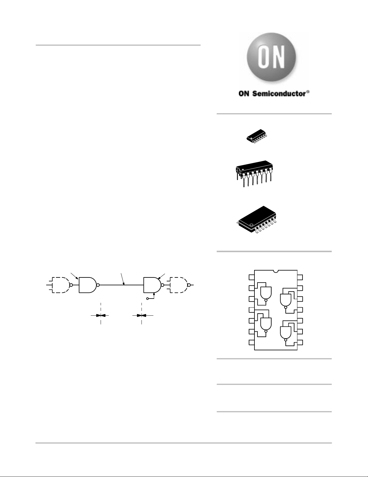
http://onsemi.com
14
1
14
1
1
SOIC−14
D SUFFIX
CASE 751A
PDIP−14
P SUFFIX
CASE 646
Line Driver
MC1488
MDTL Logic Input
Interconnecting
Cable
Interconnecting
Cable
MDTL Logic Output
Figure 1. Simplified Application
Line Receiver
MC1489
14
1
SOEIAJ−14
M SUFFIX
CASE 965
PIN CONNECTIONS
V
Input A
Output A
Input B1
Input B2
Output B
Gnd
1
EE
2
3
4
5
6
7
14
13
12
11
10
9
8
V
CC
Input D1
Input D2
Output D
Input C1
Input C2
Output C
ORDERING INFORMATION
See detailed ordering and shipping information in the package
dimensions section on page 8 of this data sheet.
DEVICE MARKING INFORMATION
See general marking information in the device marking
section on page 8 of this data sheet.
Semiconductor Components Industries, LLC, 2004
September, 2004 − Rev. 7
*For additional information on our Pb−Free strategy
and soldering details, please download the
ON Semiconductor Soldering and Mounting
Techniques Reference Manual, SOLDERRM/D.
1 Publication Order Number:
MC1488/D
Page 2
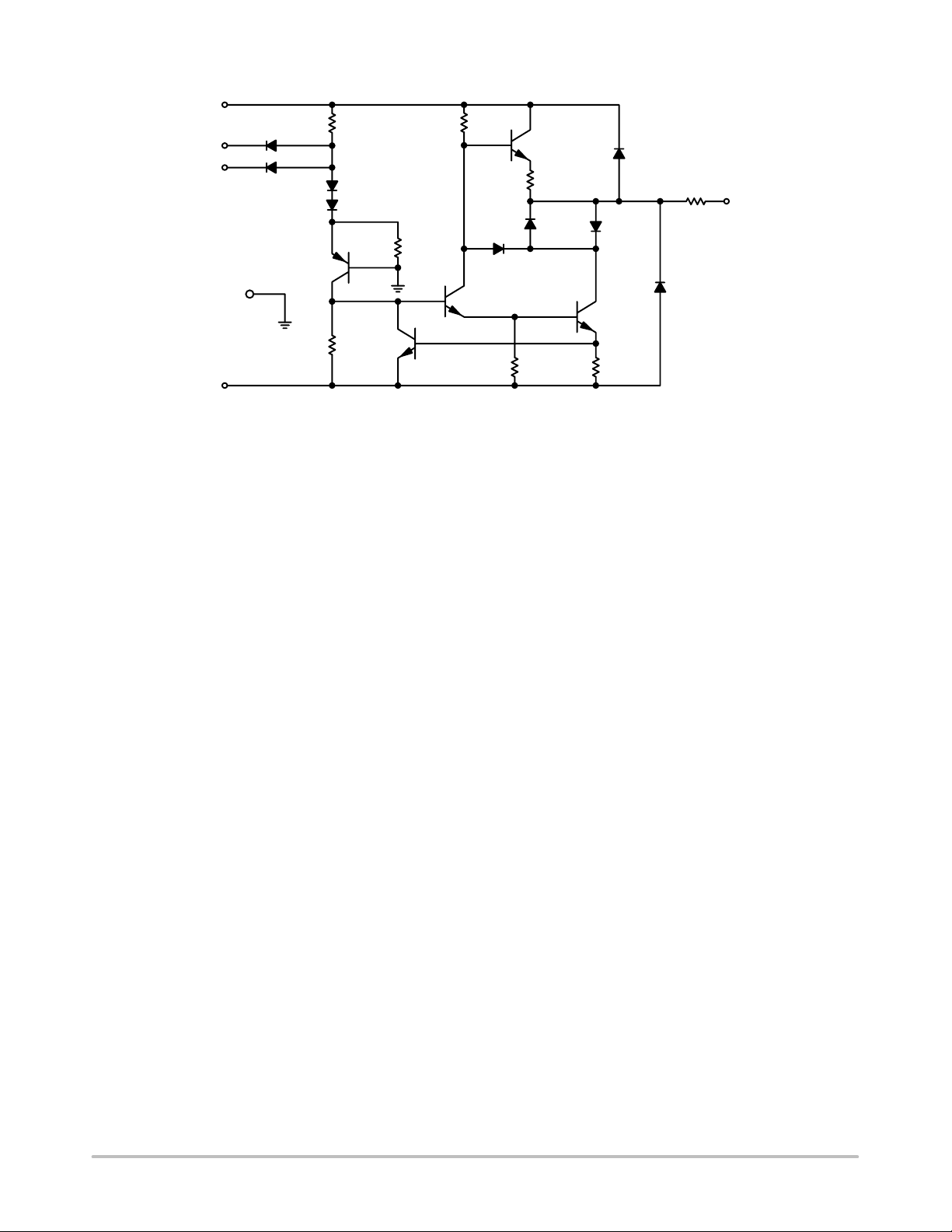
14
V
CC
Pins 4, 9, 12 or 2
Input
Input
Pins 5, 10, 13
GND 7
VEE 1
10 k
MC1488
8.2 k
3.6 k
Figure 2. Circuit Schematic
(1/4 of Circuit Shown)
6.2 k
70
7.0 k 70
300
Output
Pins 6, 8, 11 or 3
http://onsemi.com
2
Page 3
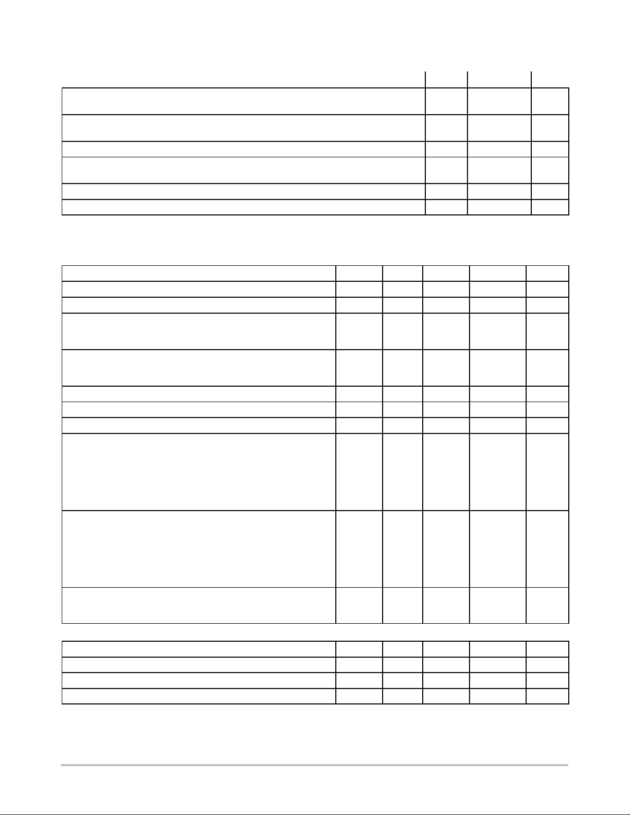
MC1488
MAXIMUM RATINGS (T
Power Supply Voltage V
Input Voltage Range V
= + 25°C, unless otherwise noted.)
A
Rating Symbol
Value Unit
CC
V
EE
IR
+ 15
− 15
− 15 VIR
Vdc
Vdc
7.0
Output Signal Voltage V
Power Derating (Package Limitation, SO−14 and Plastic Dual−In−Line Package)
Derate above T
= + 25°C
A
1/R
Operating Ambient Temperature Range T
Storage Temperature Range T
O
P
D
JA
A
stg
± 15 Vdc
1000
6.7
mW
mW/°C
0 to + 75 °C
− 65 to + 175 °C
Maximum ratings are those values beyond which device damage can occur. Maximum ratings applied to the device are individual stress limit
values (not normal operating conditions) and are not valid simultaneously . If these limits are exceeded, device functional operation is not implied,
damage may occur and reliability may be affected.
ELECTRICAL CHARACTERISTICS (V
= + 9.0 ± 1% Vdc, VEE = − 9.0 ± 1% Vdc, TA = 0 to 75°C, unless otherwise noted.)
CC
Characteristic Symbol Min Typ Max Unit
Input Current − Low Logic State (VIL = 0) I
Input Current − High Logic State (VIH = 5.0 V) I
Output Voltage − High Logic State
(V
= 0.8 Vdc, RL = 3.0 k , VCC = + 9.0 Vdc, VEE = − 9.0 Vdc)
IL
= 0.8 Vdc, RL = 3.0 k , VCC = + 13.2 Vdc, VEE = − 13.2 Vdc)
(V
IL
Output Voltage − Low Logic State
= 1.9 Vdc, RL = 3.0 k , VCC = + 9.0 Vdc, VEE = − 9.0 Vdc)
(V
IH
(V
= 1.9 Vdc, RL = 3.0 k , VCC = + 13.2 Vdc, VEE = − 13.2 Vdc)
IH
Positive Output Short−Circuit Current, Note 1 I
Negative Output Short−Circuit Current, Note 1 I
Output Resistance (VCC = VEE = 0, VO = ± 2.0 V) r
Positive Supply Current (RI = ∞)
(V
= 1.9 Vdc, VCC = + 9.0 Vdc)
IH
= 0.8 Vdc, VCC = + 9.0 Vdc)
(V
IL
= 1.9 Vdc, VCC = + 12 Vdc)
(V
IH
(V
= 0.8 Vdc, VCC = + 12 Vdc)
IL
= 1.9 Vdc, VCC = + 15 Vdc)
(V
IH
= 0.8 Vdc, VCC = + 15 Vdc)
(V
IL
Negative Supply Current (RL = ∞)
(V
= 1.9 Vdc, VEE = − 9.0 Vdc)
IH
= 0.8 Vdc, VEE = − 9.0 Vdc)
(V
IL
(V
= 1.9 Vdc, VEE = − 12 Vdc)
IH
= 0.8 Vdc, VEE = − 12 Vdc)
(V
IL
(V
= 1.9 Vdc, VEE = − 15 Vdc)
IH
= 0.8 Vdc, VEE = − 15 Vdc)
(V
IL
Power Consumption
(V
= 9.0 Vdc, VEE = − 9.0 Vdc)
CC
= 12 Vdc, VEE = − 12 Vdc)
(V
CC
SWITCHING CHARACTERISTICS (V
= + 9.0 ± 1% Vdc, VEE = − 9.0 ± 1% Vdc, TA = + 25°C.)
CC
Propagation Delay Time (zI = 3.0 k and 15 pF) t
Fall Time (zI = 3.0 k and 15 pF) t
Propagation Delay Time (zI = 3.0 k and 15 pF) t
Rise Time (zI = 3.0 k and 15 pF) t
V
V
OS +
OS −
I
CC
I
EE
P
PLH
THL
PHL
TLH
IL
IH
OH
OL
o
C
− 1.0 1.6 mA
− − 10 A
Vdc
+ 6.0
+ 9.0
+ 7.0
+ 10.5
−
−
Vdc
− 6.0
− 9.0
− 7.0
− 10.5
−
−
+ 6.0 + 10 + 12 mA
− 6.0 − 10 − 12 mA
300 − − Ohms
mA
−
−
−
−
−
−
−
−
−
−
−
−
+ 15
+ 4.5
+ 19
+ 5.5
−
−
− 13
−
− 18
−
−
−
+ 20
+ 6.0
+ 25
+ 7.0
+ 34
+ 12
− 17
− 500
− 23
− 500
− 34
− 2.5
mA
A
mA
A
mA
mA
mW
−
−
−
−
333
576
− 275 350 ns
− 45 75 ns
− 110 175 ns
− 55 100 ns
1. Maximum Package Power Dissipation may be exceeded if all outputs are shorted simultaneously.
http://onsemi.com
3
Page 4

9.0 V
MC1488
CHARACTERISTIC DEFINITIONS
−9.0 V
1
14
1.9 V
9.0 V
14 1
−9.0 V
I
I
OS +
OS −
I
IL
1.9 V
2
4
9
12
7
I
IH
5
V
10
OL
V
OH
13
0.8 V
2
4
9
12
3
6
8
11
7
5.0 V
Figure 3. Input Voltage Figure 4. Output Current
V
V
EE
CC
14
1
2
4
9
12
3
6
I
±
OS
8
11
14
2
4
5
9
10
1
7
3
6
8
11
13
12
3.0 k
V
OH
V
OL
V
O
± 2.0 Vdc
± 6.6 mA Max
0.8 V
7
Figure 5. Output Short−Circuit Current Figure 6. Output Resistance (Power Off)
V
CC
e
I
1.9 V
2
V
IH
V
IL
4
9
12
0.8 V
CC
14
7
1
I
EE
V
EE
in
3.0 V
1.5 V
e
in
V
O
t
PHL
t
PLH
50%
t
THL
t
and t
THL
Measured 10% to 90%
TLH
t
TLH
Figure 7. Power Supply Currents Figure 8. Switching Response
V
O
15 pF3.0 k
0 V
http://onsemi.com
4
Page 5

MC1488
TYPICAL CHARACTERISTICS
(TA = +25°C, unless otherwise noted.)
12
9.0
6.0
3.0
−3.0
−6.0
O
V , OUTPUT VOLTAGE (V)
V
I
0
3.0 k
V
O
−9.0
−12
0
Vin, INPUT VOLTAGE (V)
Figure 9. Transfer Characteristics
versus Power Supply Voltage
1000
100
10
V
SLEW RATE (V/s)µ
I
1.0
1.0 100 10,0001,000
10
C
V
O
C
L
, CAPACITANCE (pF)
L
Figure 11. Output Slew Rate
versus Load Capacitance
VCC = V
VCC = V
VCC = V
= ± 12 V
EE
EE
= ± 9.0 V
= ± 6.0 V
EE
12
9.0
I
OS +
6.0
V
3.0
−3.0
1.9 V
0
V
I
0.8 V
= 9.0 V
CC
VEE = 9.0 V
−6.0
I
−9.0
−12
SC
2.01.81.61.41.20.40.2 0.6 0.8 1.0
I , SHORT CIRCUIT OUTPUT CURRENT (mA)
OS −
75−55 0 25
125
T, TEMPERATURE (°C)
Figure 10. Short Circuit Output Current
versus Temperature
20
12
8.0
3.0 k LOAD LINE
4.0
0
−4.0
1.9 V
−8.0
O
I , OUTPUT CURRENT (mA)
−12
−16
−20
0.8 V
V
I
VCC = V
I
OS
+
= ± 9.0V
EE
−
0
V
, OUTPUT VOLTAGE (V)
O
V
O
16−16 −12 −8.0 12−4.0 4.0168.0
Figure 12. Output Voltage and
Current−Limiting Characteristics
16
14
V
CC
12
10
8.0
6.0
4.0
EE
2.0
CC
V , V , POWER SUPPLY VOLTAGE (V)
0
14
3.0 k
3
3.0 k
6
3.0 k
8
3.0 k
11
7
1
V
EE
25
−55 12575
0
T, TEMPERATURE (°C)
Figure 13. Maximum Operating T emperature
versus Power Supply Voltage
http://onsemi.com
5
Page 6

MC1488
APPLICATIONS INFORMATION
The Electronic Industries Association EIA−232D
specification details the requirements for the interface
between data processing equipment and data
communications equipment. This standard specifies not
only the number and type of interface leads, but also the
voltage levels to be used. The MC1488 quad driver and its
companion circuit, the MC1489 quad receiver, provide a
complete interface system between DTL or TTL logic levels
and the EIA−232D defined levels. The EIA−232D
requirements as applied to drivers are discussed herein.
The required driver voltages are defined as between
5.0 and 1 5 V in magnitude a nd are positive for a Logic “0”
and negative f or a Logic “ 1.” T hese voltages are so defined
when the drivers are terminated with a 3000 to 7000
resistor. The MC1488 meets this voltage requirement by
converting a DTL/TTL logic level into EIA−232D levels
with one stage of inversion.
The EIA−232D specification further requires that
during transitions, the driver output slew rate must not
exceed 30 V p er m icrosecond. The i nherent s lew r ate of t he
MC1488 is m uch too fast f or t his requirement. The c urrent
limited output of the device can be u sed t o c ontrol this s lew
rate by connecting a capacitor to each driver output. The
required capacitor can be easily determined by using the
relationship C = I
x T/V from which Figure 14 is
OS
derived. Accordingly, a 330 pF capacitor on each output
will guarantee a worst case slew rate of 30 V per
microsecond.
power supply d esigns, a loss of s ystem p ower causes a l ow
impedance on the power s upply outputs. When this occurs,
a low i mpedance to ground w ould e xist at the p ower i nputs
to the MC1488 effectively shorting the 300 output
resistors to ground. If all four outputs
were then s horted to
plus or minus 15 V, the power dissipation in these resistors
would be excessive. Therefore, if the system is designed to
permit low impedances to ground at the power supplies of
the drivers, a diode should be placed in each power supply
lead to prevent overheating in this fault condition. These two
diodes, as shown in Figure 15, could be used to decouple all
the driver packages in a system. (These same diodes will
allow the MC1488 to withstand momentary shorts to the
±25 V limits specified i n the earlier Standard EIA−232B.)
The addition of the diodes also permits the MC1488 to
withstand faults with power supplies of less than the 9.0 V
stated above.
V
CC
14
MC1488
MC1488
14
14
MC1488
1000
100
30 V/s
10
SLEW RATE (V/s)µ
333 pF
1.0
Figure 14. Slew Rate versus Capacitance
10
C, CAPACITANCE (pF)
for I
SC
= 10 mA
10,000100 1,0001.0
The interface driver is also required to withstand an
accidental short to any other conductor in an
interconnecting cable. The worst possible signal on any
conductor would be another driver using a plus or minus
15 V, 500 mA source. The MC1488 is designed to
indefinitely withstand such a short to all four outputs in a
package as long as the power supply voltages are greater
than 9.0 V (i.e., V
9.0 V; VEE − 9.0 V). In some
CC
V
7
EE
Figure 15. Power Supply Protection
to Meet Power Off Fault Conditions
71 171
The maximum short circuit current allowable under
fault conditions is more than guaranteed by the previously
mentioned 10 mA output current limiting.
Other Applications
The MC1488 is an extremely versatile line driver with
a myriad of possible applications. Several features of the
drivers enhance this versatility:
1. Output Current Limiting − this enables the circuit
designer to d efine t he output voltage l evels independent of
power supplies and can be accomplished by diode
clamping of the output pins. Figure 16 shows the MC1488
used as a DTL to MOS translator where the high level
voltage output is clamped one diode above ground. The
resistor divider shown i s used to reduce the output voltage
below the 300 mV above ground MOS input level limit.
http://onsemi.com
6
Page 7

MC1488
2. Power Supply Range − as can be seen from the
schematic drawing of the drivers, the positive and negative
driving elements of the device are essentially independent
and do not require matching power supplies. In fact, the
positive supply c an v ary f rom a m inimum 7 .0 V (required for
driving the negative pulldown section) to the maximum
specified 15 V. The negative supply can vary from
approximately − 2.5 V to the minimum specified − 15 V. The
12 V
MDTL
MTTL
Input
1/4 MC1488
MOS Output
(with V
1.0 k
10 k
−12 V−12 V
SS
Figure 16. MDTL/MTTL−to−MOS Translator
= GND)
MC1488 will drive the output to within 2.0 V o f the p ositive
or negative s upplies a s l ong a s t he c urrent o utput l imits a re n ot
exceeded. The c ombination o f t he c urrent l imiting a nd s upply
voltage features allow a w ide c ombination o f p ossible outputs
within the same quad package. Thus if only a portion of the
four drivers are used for driving EIA−232D lines, the
remainder could be used for DTL to MOS or even DTL to
DTL translation. Figure 17 shows one such combination.
MDTL
Input
MDTL
NAND
Gate
Input
MDTL
MHTL
Input
MDTL
MMOS
Input
2
4
5
MC1488
9
10
12
13
1
3
6
8
11
147
3.0 V
5.0 V
1.0 k
10 k
MRTL Output
−0.7 V to +3.7 V
MDTL Output
−0.7 V to +5.7 V
MHTL Output
−0.7 V to 10 V
MOS Output
−10 V to 0 V
−12 V
12 V
Figure 17. Logic Translator Applications
http://onsemi.com
7
Page 8

ORDERING INFORMATION
T
C
Device Package Operating Temperature Range Shipping
MC1488D
MC1488DR2
MC1488DR2G
MC1488P
MC1488PG
MC1488M
MC1488M
MC1488MEL
MC1488MEL
SOIC−14
SOIC−14
(Pb−Free)
PDIP−14
PDIP−14
(Pb−Free)
SOEIAJ−14
SOEIAJ−14
(Pb−Free)
SOEIAJ−14
SOEIAJ−14
(Pb−Free)
MARKING DIAGRAMS
MC1488
= 0 to +75°
A
TA = 0 to +75°C
TA = 0 to +75°C
°
55 Units/Rail
2500 Tape & Reel
2500 Tape & Reel
500 Units/Rail
500 Units/Rail
50 Units/Rail
50 Units/Rail
2000 Tape & Reel
2000 Tape & Reel
14
MC1488AD
AWLYWW
1
SOIC−14
D SUFFIX
CASE 751A
14
1
MC1488D
AWLYWW
14
1
SOEIAJ−14
M SUFFIX
CASE 965
MC1488A
ALYW
A = Assembly Location
WL, L = Wafer Lot
YY, Y = Year
WW, W = Work Week
MC1488AP
AWLYYWW
MC1488
ALYW
PDIP−14
P SUFFIX
CASE 646
14
MC1488P
AWLYYWW
1
http://onsemi.com
8
Page 9

−T−
SEATING
PLANE
MC1488
PACKAGE DIMENSIONS
SOIC−14
D SUFFIX
CASE 751A−03
ISSUE G
−A−
14
1
G
D 14 PL
0.25 (0.010) A
8
−B−
7
M
7 PL
P
M
0.25 (0.010) B
R
C
X 45
K
S
B
T
S
M
M
J
NOTES:
1. DIMENSIONING AND TOLERANCING PER
ANSI Y14.5M, 1982.
2. CONTROLLING DIMENSION: MILLIMETER.
3. DIMENSIONS A AND B DO NOT INCLUDE
MOLD PROTRUSION.
4. MAXIMUM MOLD PROTRUSION 0.15 (0.006)
PER SIDE.
5. DIMENSION D DOES NOT INCLUDE
DAMBAR PROTRUSION. ALLOWABLE
DAMBAR PROTRUSION SHALL BE 0.127
(0.005) TOTAL IN EXCESS OF THE D
DIMENSION AT MAXIMUM MATERIAL
CONDITION.
F
DIM MIN MAX MIN MAX
A 8.55 8.75 0.337 0.344
B 3.80 4.00 0.150 0.157
C 1.35 1.75 0.054 0.068
D 0.35 0.49 0.014 0.019
F 0.40 1.25 0.016 0.049
G 1.27 BSC 0.050 BSC
J 0.19 0.25 0.008 0.009
K 0.10 0.25 0.004 0.009
M 0 7 0 7
P 5.80 6.20 0.228 0.244
R 0.25 0.50 0.010 0.019
INCHESMILLIMETERS
−T−
SEATING
PLANE
14 8
17
N
HG
PDIP−14
P SUFFIX
CASE 646−06
ISSUE N
NOTES:
1. DIMENSIONING AND TOLERANCING
PER ANSI Y14.5M, 1982.
2. CONTROLLING DIMENSION: INCH.
B
A
F
L
C
14 PL
D
0.13 (0.005)
K
J
M
M
3. DIMENSION L TO CENTER OF LEADS
WHEN FORMED PARALLEL.
4. DIMENSION B DOES NOT INCLUDE
MOLD FLASH.
5. ROUNDED CORNERS OPTIONAL.
DIM MIN MAX MIN MAX
A 0.715 0.770 18.16 18.80
B 0.240 0.260 6.10 6.60
C 0.145 0.185 3.69 4.69
D 0.015 0.021 0.38 0.53
F 0.040 0.070 1.02 1.78
G 0.100 BSC 2.54 BSC
H 0.052 0.095 1.32 2.41
J 0.008 0.015 0.20 0.38
K 0.115 0.135 2.92 3.43
L
0.290 0.310 7.37 7.87
M −−− 10 −−− 10
N 0.015 0.039 0.38 1.01
MILLIMETERSINCHES
http://onsemi.com
9
Page 10

14 8
1
Z
D
e
b
0.13 (0.005)
M
E
7
A
0.10 (0.004)
H
A
1
E
VIEW P
MC1488
PACKAGE DIMENSIONS
SOEIAJ−14
M SUFFIX
CASE 965−01
ISSUE O
L
E
Q
1
M
L
DETAIL P
NOTES:
1. DIMENSIONING AND TOLERANCING PER ANSI
Y14.5M, 1982.
2. CONTROLLING DIMENSION: MILLIMETER.
3. DIMENSIONS D AND E DO NOT INCLUDE MOLD
FLASH OR PROTRUSIONS AND ARE MEASURED
AT THE PARTING LINE. MOLD FLASH OR
PROTRUSIONS SHALL NOT EXCEED 0.15 (0.006)
PER SIDE.
4. TERMINAL NUMBERS ARE SHOWN FOR
REFERENCE ONLY.
5. THE LEAD WIDTH DIMENSION (b) DOES NOT
INCLUDE DAMBAR PROTRUSION. ALLOWABLE
DAMBAR PROTRUSION SHALL BE 0.08 (0.003)
TOTAL IN EXCESS OF THE LEAD WIDTH
DIMENSION AT MAXIMUM MATERIAL CONDITION.
DAMBAR CANNOT BE LOCATED ON THE LOWER
RADIUS OR THE FOOT. MINIMUM SPACE
c
BETWEEN PROTRUSIONS AND ADJACENT LEAD
TO BE 0.46 ( 0.018).
MILLIMETERS
DIM MIN MAX MIN MAX
−−− 2.05 −−− 0.081
A
A
0.05 0.20 0.002 0.008
1
0.35 0.50 0.014 0.020
b
0.18 0.27 0.007 0.011
c
9.90 10.50 0.390 0.413
D
5.10 5.45 0.201 0.215
E
1.27 BSC 0.050 BSC
e
H
7.40 8.20 0.291 0.323
E
0.50 0.85 0.020 0.033
0.50
L
1.10 1.50 0.043 0.059
E
0
M
Q
0.70 0.90 0.028 0.035
1
−−− 1.42 −−− 0.056
Z
INCHES
10
10
0
ON Semiconductor and are registered trademarks of Semiconductor Components Industries, LLC (SCILLC). SCILLC reserves the right to make changes without further notice
to any products herein. SCILLC makes no warranty, representation or guarantee regarding the suitability of its products for any particular purpose, nor does SCILLC assume any liability
arising out of the application or use of any product or circuit, and specifically disclaims any and all liability, including without limitation special, consequential or incidental damages.
“Typical” parameters which may be provided in SCILLC data sheets and/or specifications can and do vary in different applications and actual performance may vary over time. All
operating parameters, including “Typicals” must be validated for each customer application by customer’s technical experts. SCILLC does not convey any license under its patent rights
nor the rights of others. SCILLC products are not designed, intended, or authorized for use as components in systems intended for surgical implant into the body, or other applications
intended to support or sustain life, or for any other application in which the failure of the SCILLC product could create a situation where personal injury or death may occur. Should
Buyer purchase or use SCILLC products for any such unintended or unauthorized application, Buyer shall indemnify and hold SCILLC and its officers, employees, subsidiaries, affiliates,
and distributors harmless against all claims, costs, damages, and expenses, and reasonable attorney fees arising out of, directly or indirectly, any claim of personal injury or death
associated with such unintended or unauthorized use, even if such claim alleges that SCILLC was negligent regarding the design or manufacture of the part. SCILLC is an Equal
Opportunity/Affirmative Action Employer. This literature is subject to all applicable copyright laws and is not for resale in any manner.
PUBLICATION ORDERING INFORMATION
LITERATURE FULFILLMENT:
Literature Distribution Center for ON Semiconductor
P.O. Box 61312, Phoenix, Arizona 85082−1312 USA
Phone: 480−829−7710 or 800−344−3860 Toll Free USA/Canada
Fax: 480−829−7709 or 800−344−3867 Toll Free USA/Canada
Email: orderlit@onsemi.com
N. American Technical Support: 800−282−9855 Toll Free
USA/Canada
Japan: ON Semiconductor, Japan Customer Focus Center
2−9−1 Kamimeguro, Meguro−ku, Tokyo, Japan 153−0051
Phone: 81−3−5773−3850
http://onsemi.com
ON Semiconductor Website: http://onsemi.com
Order Literature: http://www.onsemi.com/litorder
For additional information, please contact your
local Sales Representative.
MC1488/D
10
 Loading...