

Page 1
MC10EP90, MC100EP90
Translator, Triple ECL Input to
LVPECL / PECL Output
Description
The MC
translator. The device receives differential LVECL or ECL signals and
translates them to differential LVPECL or PECL output signals.
A VBB output is provided for interfacing with Single−Ended LVECL or
VBB output should be connected to the D input. The active signal would
then drive the D input. When used the VBB output should be bypassed
to ground by a 0.01 mF capacitor. The VBB output is designed to act as
the switching reference for the EP90 under Single−Ended input
switching conditions, as a result this pin can only source/sink up to 0.5
mA of current.
To accomplish the level translation the EP90 requires three power
rails. The VCC supply should be connected to the positive supply, and
the VEE connected to the negative supply.
The 100 Series contains temperature compensation.
Features
• 260 ps Typical Propagation Delay
• Maximum Frequency > 3 GHz Typical
• Voltage Supplies V
GND = 0 V
• Open Input Default State
• Safety Clamp on Inputs
• Fully Differential Design
• Q Output Will Default LOW with Inputs Open or at V
• V
• These are Pb−Free Devices*
10/100EP90 is a TRIPLE ECL TO LVPECL/PECL
ECL signals at the input. If a Single−Ended input is to be used the
= 3.0 V to 5.5 V, VEE = −3.0 V to −5.5 V,
CC
EE
Output
BB
http://onsemi.com
TSSOP−20
DT SUFFIX
CASE 948E
MARKING DIAGRAM*
20
xxxx
EP90
ALYWG
G
1
xxxx = MC10 or 100
A = Assembly Location
L = Wafer Lot
Y = Year
W = Work Week
G = Pb−Free Package
(Note: Microdot may be in either location)
*For additional marking information, refer to
Application Note AND8002/D.
*For additional information on our Pb−Free strategy and soldering details, please
download the ON Semiconductor Soldering and Mounting Techniques
Reference Manual, SOLDERRM/D.
© Semiconductor Components Industries, LLC, 2014
May, 2014 − Rev. 7
1 Publication Order Number:
ORDERING INFORMATION
See detailed ordering and shipping information in the package
dimensions section on page 7 of this data sheet.
MC10EP90/D
Page 2
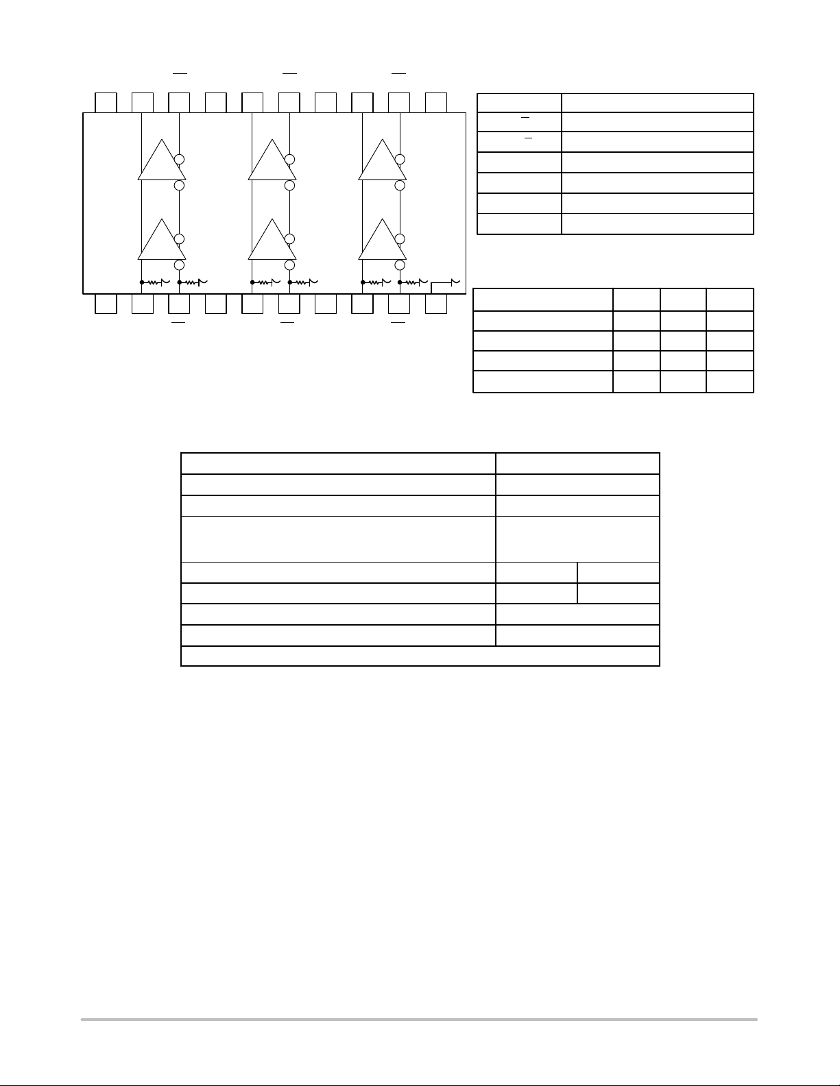
MC10EP90, MC100EP90
Q0
GND Q1 GND Q2 Q2 V
V
Q0
Q1
CC
1718 16 15 14 13 12
LVPECL/
PECL
ECL
LVPECL/
PECL
ECL
43 56789
BB
D1V
D1D0
D2V
V
BB
D2
LVPECL/
PECL
ECL
CC
1920
21
D0
Warning: All VCC, VEE and GND pins must be externally connected to
Power Supply to guarantee proper operation.
Figure 1. TSSOP−20 (Top View) and Logic Diagram
Table 3. ATTRIBUTES
Characteristics Value
Internal Input Pulldown Resistor
Internal Input Pullup Resistor N/A
ESD Protection Human Body Model
Charged Device Model
Moisture Sensitivity, Indefinite Time Out of Drypack (Note 1) Pb Pkg Pb−Free Pkg
Flammability Rating Oxygen Index: 28 to 34 UL 94 V−0 @ 0.125 in
Transistor Count 350 Devices
Meets or exceeds JEDEC Spec EIA/JESD78 IC Latchup Test
1. For additional information, refer to Application Note AND8003/D.
CC
11
Table 1. PIN DESCRIPTION
PIN
Q(0:2), Q
FUNCTION
(0:2)
Differential LVPECL or PECL Outputs
D(0:2)*, D(0:2)* Differential LVECL or ECL Inputs
V
CC
Positive Supply
GND Ground
V
EE
V
BB
Negative Supply
Output Reference Supply
* Pins will default LOW when left open.
Table 2. FUNCTION TABLE
10
V
EE
Machine Model
TSSOP−20 Level 1 Level 1
Function V
−5V ECL to 5V PECL
−5V ECL to 3.3V PECL
−3.3V ECL to 5V PECL
−3.3V ECL to 3.3V PECL
75 kW
> 2 kV
> 200 V
> 2 kV
CC
5 V
3.3 V
5 V
3.3 V
GND
0 V
0 V
0 V
0 V
V
EE
−5 V
−5 V
−3.3 V
−3.3 V
http://onsemi.com
2
Page 3
MC10EP90, MC100EP90
Table 4. MAXIMUM RATINGS
Symbol Parameter Condition 1 Condition 2 Rating Unit
V
CC
V
EE
V
I
I
out
I
BB
T
A
T
stg
q
JA
q
JC
T
sol
Stresses exceeding Maximum Ratings may damage the device. Maximum Ratings are stress ratings only. Functional operation above the
Recommended Operating Conditions is not implied. Extended exposure to stresses above the Recommended Operating Conditions may affect
device reliability.
PECL Mode Power Supply GND = 0 V 6 V
NECL Mode Power Supply GND = 0 V −6 V
PECL Mode Input Voltage
NECL Mode Input Voltage
Output Current Continuous
GND = 0 V
GND = 0 V
Surge
VI V
VI V
CC
EE
6
−6
50
100
V
V
mA
mA
VBB Sink/Source ± 0.5 mA
Operating Temperature Range −40 to +85 °C
Storage Temperature Range −65 to +150 °C
Thermal Resistance (Junction−to−Ambient) 0 lfpm
500 lfpm
TSSOP−20
TSSOP−20
140
100
°C/W
°C/W
Thermal Resistance (Junction−to−Case) Standard Board TSSOP−20 23 to 41 °C/W
Wave Solder Pb
Pb−Free
<2 to 3 sec @ 248°C
<2 to 3 sec @ 260°C
265
265
°C
http://onsemi.com
3
Page 4

MC10EP90, MC100EP90
l
l
Table 5. 10EP DC CHARACTERISTICS V
= 3.3 V, V
CC
= −5.5 V to −3.0 V; GND = 0 V (Note 2)
EE
−40°C 25°C 85°C
Symbo
I
EE
I
CC
V
OH
V
OL
V
IH
V
IL
V
BB
V
IHCMR
Characteristic
Negative Power Supply Current 5 13 20 5 13 20 5 13 20 mA
Positive Power Supply Current 43 55 67 43 55 67 43 55 67 mA
Output HIGH Voltage (Note 3) 2165 2290 2415 2230 2355 2480 2290 2415 2540 mV
Output LOW Voltage (Note 3) 1365 1490 1615 1430 1555 1680 1490 1615 1740 mV
Input HIGH Voltage (Single−Ended) −1210 −885 −1145 −820 −1085 −760 mV
Input LOW Voltage (Single−Ended) −1935 −1610 −1870 −1545 −1810 −1485 mV
Output Voltage Reference −1510 −1410 −1310 −1445 −1345 −1245 −1385 −1285 −1185 mV
Input HIGH Voltage Common Mode
Min Typ Max Min Typ Max Min Typ Max
VEE+2.0 0.0 VEE+2.0 0.0 VEE+2.0 0.0 V
Unit
Range (Differential Configuration)
(Note 4)
I
IH
I
IL
Input HIGH Current 150 150 150
Input LOW Current 0.5 0.5 0.5
NOTE: Device will meet the specifications after thermal equilibrium has been established when mounted in a test socket or printed circuit
board with maintained transverse airflow greater than 500 lfpm. Electrical parameters are guaranteed only over the declared
operating temperature range. Functional operation of the device exceeding these conditions is not implied. Device specification limit
values are applied individually under normal operating conditions and not valid simultaneously.
2. Input and output parameters vary 1:1 with V
3. All loading with 50 W to V
4. V
min varies 1:1 with VEE, max varies 1:1 with VCC. The V
IHCMR
signal.
− 2.0 V.
CC
CC
.
range is referenced to the most positive side of the differential input
IHCMR
mA
mA
Table 6. 10EP DC CHARACTERISTICS V
= 5.0 V, V
CC
= −5.5 V to −3.0 V; GND = 0 V (Note 5)
EE
−40°C 25°C 85°C
Symbo
I
EE
I
CC
V
OH
V
OL
V
IH
V
IL
V
BB
V
IHCMR
Characteristic
Negative Power Supply Current 5 13 20 5 13 20 5 13 20 mA
Positive Power Supply Current 43 55 67 43 55 67 43 55 67 mA
Output HIGH Voltage (Note 6) 3865 3990 4115 3930 4055 4180 3990 4115 4240 mV
Output LOW Voltage (Note 6) 3065 3190 3315 3130 3255 3380 3190 3315 3440 mV
Input HIGH Voltage (Single−Ended) −1210 −885 −1145 −820 −1085 −760 mV
Input LOW Voltage (Single−Ended) −1935 −1610 −1870 −1545 −1810 −1485 mV
Output Voltage Reference −1510 −1410 −1310 −1445 −1345 −1245 −1385 −1285 −1185 mV
Input HIGH Voltage Common Mode
Min Typ Max Min Typ Max Min Typ Max
VEE+2.0 0.0 VEE+2.0 0.0 VEE+2.0 0.0 V
Unit
Range (Differential Configuration)
(Note 7)
I
IH
I
IL
Input HIGH Current 150 150 150
Input LOW Current 0.5 0.5 0.5
NOTE: Device will meet the specifications after thermal equilibrium has been established when mounted in a test socket or printed circuit
board with maintained transverse airflow greater than 500 lfpm. Electrical parameters are guaranteed only over the declared
operating temperature range. Functional operation of the device exceeding these conditions is not implied. Device specification limit
values are applied individually under normal operating conditions and not valid simultaneously.
5. Input and output parameters vary 1:1 with V
6. All loading with 50 W to V
7. V
min varies 1:1 with VEE, max varies 1:1 with VCC. The V
IHCMR
signal.
− 2.0 V.
CC
CC
.
range is referenced to the most positive side of the differential input
IHCMR
mA
mA
http://onsemi.com
4
Page 5

MC10EP90, MC100EP90
l
l
Table 7. 100EP DC CHARACTERISTICS V
= 3.3 V, V
CC
= −5.5 V to −3.0 V; GND = 0 V (Note 8)
EE
−40°C 25°C 85°C
Symbo
I
EE
I
CC
V
OH
V
OL
V
IH
V
IL
V
BB
V
IHCMR
Characteristic
Negative Power Supply Current 5 13 20 5 13 20 5 13 20 mA
Positive Power Supply Current 45 58 70 50 62 75 53 65 78 mA
Output HIGH Voltage (Note 9) 2155 2280 2405 2155 2280 2405 2155 2280 2405 mV
Output LOW Voltage (Note 9) 1305 1480 1605 1305 1480 1605 1305 1480 1605 mV
Input HIGH Voltage (Single−Ended) −1225 −885 −1225 −885 −1225 −885 mV
Input LOW Voltage (Single−Ended) −1995 −1625 −1995 −1625 −1995 −1625 mV
Output Voltage Reference −1525 −1425 −1325 −1525 −1425 −1325 −1525 −1425 −1325 mV
Input HIGH Voltage Common Mode
Min Typ Max Min Typ Max Min Typ Max
VEE+2.0 0.0 VEE+2.0 0.0 VEE+2.0 0.0 V
Unit
Range (Differential Configuration)
(Note 10)
I
IH
I
IL
Input HIGH Current 150 150 150
Input LOW Current 0.5 0.5 0.5
NOTE: Device will meet the specifications after thermal equilibrium has been established when mounted in a test socket or printed circuit
board with maintained transverse airflow greater than 500 lfpm. Electrical parameters are guaranteed only over the declared
operating temperature range. Functional operation of the device exceeding these conditions is not implied. Device specification limit
values are applied individually under normal operating conditions and not valid simultaneously.
8. Input and output parameters vary 1:1 with V
9. All loading with 50 W to V
10.V
min varies 1:1 with VEE, max varies 1:1 with VCC. The V
IHCMR
signal.
− 2.0 V.
CC
CC
.
range is referenced to the most positive side of the differential input
IHCMR
mA
mA
Table 8. 100EP DC CHARACTERISTICS V
= 5.0 V, V
CC
= −5.5 V to −3.0 V; GND = 0 V (Note 11)
EE
−40°C 25°C 85°C
Symbo
I
EE
I
CC
V
OH
V
OL
V
IH
V
IL
V
BB
V
IHCMR
Characteristic
Negative Power Supply Current 5 13 20 5 13 20 5 13 20 mA
Positive Power Supply Current 45 58 70 50 62 75 53 65 78 mA
Output HIGH Voltage (Note 12) 3855 3980 4105 3855 3980 4105 3855 3980 4105 mV
Output LOW Voltage (Note 12) 3005 3180 3305 3005 3180 3305 3005 3180 3305 mV
Input HIGH Voltage (Single−Ended) −1225 −885 −1225 −885 −1225 −885 mV
Input LOW Voltage (Single−Ended) −1995 −1625 −1995 −1625 −1995 −1625 mV
Output Voltage Reference −1525 −1425 −1325 −1525 −1425 −1325 −1525 −1425 −1325 mV
Input HIGH Voltage Common Mode
Min Typ Max Min Typ Max Min Typ Max
VEE+2.0 0.0 VEE+2.0 0.0 VEE+2.0 0.0 V
Unit
Range (Differential Configuration)
(Note 13)
I
IH
I
IL
Input HIGH Current 150 150 150
Input LOW Current 0.5 0.5 0.5
NOTE: Device will meet the specifications after thermal equilibrium has been established when mounted in a test socket or printed circuit
board with maintained transverse airflow greater than 500 lfpm. Electrical parameters are guaranteed only over the declared
operating temperature range. Functional operation of the device exceeding these conditions is not implied. Device specification limit
values are applied individually under normal operating conditions and not valid simultaneously.
11.Input and output parameters vary 1:1 with V
12.All loading with 50 W to V
13.V
min varies 1:1 with VEE, max varies 1:1 with VCC.. The V
IHCMR
signal.
− 2.0 V.
CC
CC
.
range is referenced to the most positive side of the differential input
IHCMR
mA
mA
http://onsemi.com
5
Page 6

MC10EP90, MC100EP90
l
Table 9. AC CHARACTERISTICS V
= −3.0 V to −5.5 V; VCC = 3.0 V to 5.5 V; GND = 0 V (Note 14)
EE
−40°C 25°C 85°C
Symbo
f
max
t
,
PLH
t
PHL
t
SKEW
t
JITTER
V
PP
t
r
t
f
Characteristic
Maximum Frequency
(See Figure 2 F
max
/JITTER)
Propagation Delay to
Output Differential
Duty Cycle Skew (Note 15) 5.0 20 5.0 20 5.0 20
Within Device Skew Q, Q
Device to Device Skew (Note 15)
Cycle−to−Cycle Jitter
(See Figure 2 F
max
/JITTER)
Input Voltage
Swing (Differential Configuration)
Output Rise/Fall Times Q, Q
(20% − 80%)
Min Typ Max Min Typ Max Min Typ Max
Unit
> 3 > 3 > 3 GHz
170 240 310 200 260 340 230 300 370 ps
ps
80
140
80
140
80
140
0.2 < 1 0.2 < 1 0.2 < 1 ps
150 800 1200 150 800 1200 150 800 1200 mV
70 120 170 80 130 180 100 150 230 ps
NOTE: Device will meet the specifications after thermal equilibrium has been established when mounted in a test socket or printed circuit
board with maintained transverse airflow greater than 500 lfpm. Electrical parameters are guaranteed only over the declared
operating temperature range. Functional operation of the device exceeding these conditions is not implied. Device specification limit
values are applied individually under normal operating conditions and not valid simultaneously.
14.Measured using a 750 mV source, 50% duty cycle clock source. All loading with 50 W to V
15.Skew is measured between outputs under identical transitions. Duty cycle skew is defined only for differential operation when the delays
CC
−2.0 V.
are measured from the cross point of the inputs to the cross point of the outputs.
900
800
700
(mV)
600
OUTpp
500
V
400
300
200
100
(JITTER)
0
0 1000 2000 3000 4000 5000
FREQUENCY (MHz)
Figure 2. F
max
/Jitter
9
8
7
6
5
4
3
2
1
ps (RMS)
OUT
JITTER
http://onsemi.com
6
Page 7

MC10EP90, MC100EP90
Zo = 50 W
Zo = 50 W
50 W 50 W
V
VTT = VCC − 2.0 V
TT
Receiver
Device
Driver
Device
QD
Q D
Figure 3. Typical Termination for Output Driver and Device Evaluation
(See Application Note AND8020/D − Termination of ECL Logic Devices.)
ORDERING INFORMATION
Device Package Shipping
MC10EP90DTG
MC10EP90DTR2G 2500 / Tape & Rail
MC100EP90DTG 75 Units / Rail
MC100EP90DTR2G 2500 / Tape & Rail
†For information on tape and reel specifications, including part orientation and tape sizes, please refer to our Tape and Reel Packaging
Specifications Brochure, BRD8011/D.
TSSOP−20
(Pb−Free)
75 Units / Rail
†
Resource Reference of Application Notes
AN1405/D − ECL Clock Distribution Techniques
AN1406/D − Designing with PECL (ECL at +5.0 V)
AN1503/D −
AN1504/D − Metastability and the ECLinPS Family
AN1568/D − Interfacing Between LVDS and ECL
AN1672/D − The ECL Translator Guide
AND8001/D − Odd Number Counters Design
AND8002/D − Marking and Date Codes
AND8020/D − Termination of ECL Logic Devices
AND8066/D − Interfacing with ECLinPS
AND8090/D − AC Characteristics of ECL Devices
ECLinPSt I/O SPiCE Modeling Kit
ECLinPS is a trademark of Semiconductor Components Industries, LLC (SCILLC).
http://onsemi.com
7
Page 8

MECHANICAL CASE OUTLINE
PACKAGE DIMENSIONS
TSSOP−20 WB
CASE 948E
ISSUE D
DATE 17 FEB 2016
SCALE 2:1
L
20X REFK
S
U0.15 (0.006) T
2X
L/2
PIN 1
IDENT
110
S
U0.15 (0.006) T
C
D
0.100 (0.004)
SEATING
−T−
PLANE
SOLDERING FOOTPRINT
1
0.10 (0.004) V
M
S
U
T
1120
−U−
A
−V−
G
H
7.06
NOTES:
S
K1
JJ1
K
B
SECTION N−N
N
0.25 (0.010)
M
N
F
DETAIL E
DETAIL E
1. DIMENSIONING AND TOLERANCING PER
ANSI Y14.5M, 1982.
2. CONTROLLING DIMENSION: MILLIMETER.
3. DIMENSION A DOES NOT INCLUDE MOLD
FLASH, PROTRUSIONS OR GATE BURRS.
MOLD FLASH OR GATE BURRS SHALL NOT
EXCEED 0.15 (0.006) PER SIDE.
4. DIMENSION B DOES NOT INCLUDE
INTERLEAD FLASH OR PROTRUSION.
INTERLEAD FLASH OR PROTRUSION
SHALL NOT EXCEED 0.25 (0.010) PER SIDE.
5. DIMENSION K DOES NOT INCLUDE
DAMBAR PROTRUSION. ALLOWABLE
DAMBAR PROTRUSION SHALL BE 0.08
(0.003) TOTAL IN EXCESS OF THE K
DIMENSION AT MAXIMUM MATERIAL
CONDITION.
6. TERMINAL NUMBERS ARE SHOWN FOR
REFERENCE ONLY.
7. DIMENSION A AND B ARE TO BE
DETERMINED AT DATUM PLANE −W−.
INCHES
6.60 0.260
−W−
MILLIMETERS
DIMAMIN MAX MIN MAX
6.40 0.252
B 4.30 4.50 0.169 0.177
C 1.20 0.047
--- ---
D 0.05 0.15 0.002 0.006
F 0.50 0.75 0.020 0.030
G 0.65 BSC 0.026 BSC
H 0.27 0.37 0.011 0.015
J 0.09 0.20 0.004 0.008
J1 0.09 0.16 0.004 0.006
K 0.19 0.30 0.007 0.012
K1 0.19 0.25 0.007 0.010
L 6.40 BSC 0.252 BSC
M 0 8 0 8
____
GENERIC
MARKING DIAGRAM*
XXXX
XXXX
ALYWG
G
A = Assembly Location
L = Wafer Lot
Y = Year
W = Work Week
G = Pb−Free Package
0.65
PITCH
(Note: Microdot may be in either location)
*This information is generic. Please refer to
device data sheet for actual part marking.
16X
0.36
DOCUMENT NUMBER:
DESCRIPTION:
ON Semiconductor and are trademarks of Semiconductor Components Industries, LLC dba ON Semiconductor or its subsidiaries in the United States and/or other countries.
ON Semiconductor reserves the right to make changes without further notice to any products herein. ON Semiconductor makes no warranty, representation or guarantee regarding
the suitability of its products for any particular purpose, nor does ON Semiconductor assume any liability arising out of the application or use of any product or circuit, and specifically
disclaims any and all liability, including without limitation special, consequential or incidental damages. ON Semiconductor does not convey any license under its patent rights nor the
rights of others.
© Semiconductor Components Industries, LLC, 2019
16X
1.26
98ASH70169A
TSSOP−20 WB
DIMENSIONS: MILLIMETERS
Electronic versions are uncontrolled except when accessed directly from the Document Repository.
Printed versions are uncontrolled except when stamped “CONTROLLED COPY” in red.
Pb−Free indicator, “G” or microdot “ G”,
may or may not be present.
PAGE 1 OF 1
www.onsemi.com
Page 9

ON Semiconductor and are trademarks of Semiconductor Components Industries, LLC dba ON Semiconductor or its subsidiaries in the United States and/or other countries.
ON Semiconductor owns the rights to a number of patents, trademarks, copyrights, trade secrets, and other intellectual property. A listing of ON Semiconductor’s product/patent
coverage may be accessed at www.onsemi.com/site/pdf/Patent−Marking.pdf
ON Semiconductor makes no warranty, representation or guarantee regarding the suitability of its products for any particular purpose, nor does ON Semiconductor assume any liability
arising out of the application or use of any product or circuit, and specifically disclaims any and all liability, including without limitation special, consequential or incidental damages.
Buyer is responsible for its products and applications using ON Semiconductor products, including compliance with all laws, regulations and safety requirements or standards,
regardless of any support or applications information provided by ON Semiconductor. “Typical” parameters which may be provided in ON Semiconductor data sheets and/or
specifications can and do vary in different applications and actual performance may vary over time. All operating parameters, including “Typicals” must be validated for each customer
application by customer’s technical experts. ON Semiconductor does not convey any license under its patent rights nor the rights of others. ON Semiconductor products are not
designed, intended, or authorized for use as a critical component in life support systems or any FDA Class 3 medical devices or medical devices with a same or similar classification
in a foreign jurisdiction or any devices intended for implantation in the human body. Should Buyer purchase or use ON Semiconductor products for any such unintended or unauthorized
application, Buyer shall indemnify and hold ON Semiconductor and its officers, employees, subsidiaries, affiliates, and distributors harmless against all claims, costs, damages, and
expenses, and reasonable attorney fees arising out of, directly or indirectly, any claim of personal injury or death associated with such unintended or unauthorized use, even if such
claim alleges that ON Semiconductor was negligent regarding the design or manufacture of the part. ON Semiconductor is an Equal Opportunity/Affirmative Action Employer. This
literature is subject to all applicable copyright laws and is not for resale in any manner.
. ON Semiconductor reserves the right to make changes without further notice to any products herein.
PUBLICATION ORDERING INFORMATION
LITERATURE FULFILLMENT:
Email Requests to: orderlit@onsemi.com
ON Semiconductor Website: www.onsemi.com
TECHNICAL SUPPORT
North American Technical Support:
Voice Mail: 1 800−282−9855 Toll Free USA/Canada
Phone: 011 421 33 790 2910
Europe, Middle East and Africa Technical Support:
Phone: 00421 33 790 2910
For additional information, please contact your local Sales Representative
◊
www.onsemi.com
1
 Loading...