


MC10EL51, MC100EL51
5V ECL Differential Clock D
Flip‐Flop
Description
The MC10EL/100EL51 is a differential clock D flip-flop with reset.
The device is functionally similar to the E151 device with higher
performance capabilities. With propagation delays and output
transition times significantly faster than the E151 the EL51 is ideally
suited for those applications which require the ultimate in AC
performance.
The reset input is an asynchronous, level triggered signal. Data
enters the master portion of the flip-flop when the clock is LOW and is
transferred to the slave, and thus the outputs, upon a positive transition
of the clock. The differential clock inputs of the EL51 allow the device
to be used as a negative edge triggered flip-flop.
The differential input employs clamp circuitry to maintain stability
under open input (pulled down to V
The 100 Series contains temperature compensation.
Features
• 475 ps Propagation Delay
• 2.8 GHz Toggle Frequency
• ESD Protection: > 1 kV Human Body Model,
> 100 V Machine Model
• PECL Mode Operating Range: V
EE
= 0 V
with V
• NECL Mode Operating Range: V
with V
= −4.2 V to −5.7 V
EE
• Internal Input Pulldown Resistors on D, R, and CLK
• Meets or Exceeds JEDEC Spec EIA/JESD78 IC Latchup Test
• Moisture Sensitivity Level 1
For Additional Information, see Application Note AND8003/D
• Flammability Rating: UL 94 V−0 @ 0.125 in,
Oxygen Index: 28 to 34
• Transistor Count = 73 devices
• Pb−Free Packages are Available
) conditions.
EE
= 4.2 V to 5.7 V
CC
= 0 V
CC
http://onsemi.com
MARKING
DIAGRAMS*
8
1
SOIC−8
D SUFFIX
CASE 751
8
1
TSSOP−8
DT SUFFIX
CASE 948R
DFN8
MN SUFFIX
CASE 506AA
H = MC10
K = MC100
4X = MC10
2M= MC100
A = Assembly Location
(Note: Microdot may be in either location)
*For additional marking information, refer to
Application Note AND8002/D.
8
HEL51
ALYW
1
8
HL51
ALYWG
1
14
8
G
1
8
G
L = Wafer Lot
Y = Year
W = Work Week
M
G = Pb−Free Package
1
G
4X M G
= Date Code
KEL51
ALYW
G
KL51
ALYWG
G
G
2M M G
14
© Semiconductor Components Industries, LLC, 2008
August, 2008 − Rev. 7
ORDERING INFORMATION
See detailed ordering and shipping information in the package
dimensions section on page 6 of this data sheet.
1 Publication Order Number:
MC10EL51/D

MC10EL51, MC100EL51
Table 1. TRUTH TABLE
D*
1
R
V
CC
L
H
R
D
2
D
78Q
X
Z = LOW to HIGH Transition
* Pin will default low when left open.
**Pin will default low when inputs are left open.
R*
CLK*
L
L
H
Z
Z
X
Q**
L
H
L
CLK
3
Q
6
Table 2. PIN DESCRIPTION
PIN FUNCTION
R ECL Reset Input
45
CLK
V
EE
Figure 1. Logic Diagram and Pinout Assignment
D ECL Data Input
CLK, CLK
Q, Q
V
CC
V
EE
ECL Clock Inputs
ECL Data Outputs
Positive Supply
Negative Supply
EP (DFN8 only) Thermal exposed pad
must be connected to a sufficient
thermal conduit. Electrically connect
to the most negative supply (GND)
or leave unconnected, floating open.
Table 3. MAXIMUM RATINGS
Symbol Parameter Condition 1 Condition 2 Rating Unit
V
CC
V
EE
V
I
I
out
T
A
T
stg
q
JA
q
JC
q
JA
q
JC
q
JA
T
sol
q
JC
Stresses exceeding Maximum Ratings may damage the device. Maximum Ratings are stress ratings only. Functional operation above the
Recommended Operating Conditions is not implied. Extended exposure to stresses above the Recommended Operating Conditions may affect
device reliability.
1. JEDEC standard multilayer board − 2S2P (2 signal, 2 power)
PECL Mode Power Supply VEE = 0 V 8 V
NECL Mode Power Supply VCC = 0 V −8 V
PECL Mode Input Voltage
NECL Mode Input Voltage
Output Current Continuous
VEE = 0 V
V
= 0 V
CC
Surge
VI V
VI V
CC
EE
6
−6
50
100
V
V
mA
mA
Operating Temperature Range −40 to +85 °C
Storage Temperature Range −65 to +150 °C
Thermal Resistance (Junction−to−Ambient) 0 lfpm
500 lfpm
8 SOIC
8 SOIC
190
130
°C/W
°C/W
Thermal Resistance (Junction−to−Case) Standard Board 8 SOIC 41 to 44 °C/W
Thermal Resistance (Junction−to−Ambient) 0 lfpm
500 lfpm
8 TSSOP
8 TSSOP
185
140
°C/W
°C/W
Thermal Resistance (Junction−to−Case) Standard Board 8 TSSOP 41 to 44 ± 5% °C/W
Thermal Resistance (Junction−to−Ambient) 0 lfpm
500 lfpm
Wave Solder Pb
Pb−Free
<2 to 3 sec @ 248°C
<2 to 3 sec @ 260°C
DFN8
DFN8
129
84
265
265
°C/W
°C/W
°C
Thermal Resistance (Junction−to−Case) (Note 1) DFN8 35 to 40 °C/W
http://onsemi.com
2

MC10EL51, MC100EL51
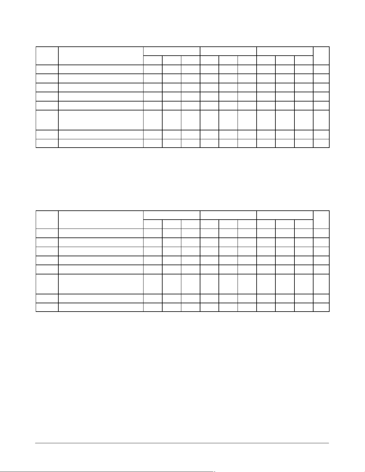
Table 4. 10EL SERIES PECL DC CHARACTERISTICS V
= 5.0 V; VEE = 0 V (Note 2)
CC
−40°C 25°C 85°C
Symbol Characteristic Min Typ Max Min Typ Max Min Ty p Max Unit
I
EE
V
OH
V
OL
V
IH
V
IL
V
IHCMR
Power Supply Current 24 29 24 29 24 29 mA
Output HIGH Voltage (Note 6) 3920 4010 4110 4020 4105 4190 4090 4185 4280 mV
Output LOW Voltage (Note 3) 3050 3200 3350 3050 3210 3370 3050 3227 3405 mV
Input HIGH Voltage (Single−Ended) 3770 4110 3870 4190 3940 4280 mV
Input LOW Voltage (Single−Ended) 3050 3500 3050 3520 3050 3555 mV
Input HIGH Voltage Common Mode
2.5 4.6 2.5 4.6 2.5 4.6 V
Range (Differential Configuration)
(Note 4)
I
IH
I
IL
Input HIGH Current 150 150 150
Input LOW Current 0.5 0.5 0.3
mA
mA
NOTE: Device will meet the specifications after thermal equilibrium has been established when mounted in a test socket or printed circuit
board with maintained transverse airflow greater than 500 lfpm. Electrical parameters are guaranteed only over the declared
operating temperature range. Functional operation of the device exceeding these conditions is not implied. Device specification limit
values are applied individually under normal operating conditions and not valid simultaneously.
2. Input and output parameters vary 1:1 with V
3. Outputs are terminated through a 50 W resistor to V
4. V
min varies 1:1 with VEE, V
IHCMR
signal. Normal operation is obtained if the HIGH level falls within the specified range and the peak-to-peak voltage lies between V
max varies 1:1 with VCC. The V
IHCMR
Table 5. 10EL SERIES NECL DC CHARACTERISTICS V
. VEE can vary +0.25 V / −0.5 V.
CC
− 2.0 V.
CC
IHCMR
= 0 V; VEE = −5.0 V (Note 5)
CC
range is referenced to the most positive side of the differential input
min and 1 V.
PP
−40°C 25°C 85°C
Symbol Characteristic Min Typ Max Min Typ Max Min Typ Max Unit
I
EE
V
OH
V
OL
V
IH
V
IL
V
IHCMR
Power Supply Current 24 29 24 29 24 29 mA
Output HIGH Voltage (Note 6) −1080 −990 −890 −980 −895 −810 −910 −815 −720 mV
Output LOW Voltage (Note 6) −1950 −1800 −1650 −1950 −1790 −1630 −1950 −1773 −1595 mV
Input HIGH Voltage (Single−Ended) −1230 −890 −1130 −810 −1060 −720 mV
Input LOW Voltage (Single−Ended) −1950 −1500 −1950 −1480 −1950 −1445 mV
Input HIGH Voltage Common Mode
−2.5 −0.4 −2.5 −0.4 −2.5 −0.4 V
Range (Differential Configuration)
(Note 7)
I
IH
I
IL
Input HIGH Current 150 150 150
Input LOW Current 0.5 0.5 0.3
mA
mA
NOTE: Device will meet the specifications after thermal equilibrium has been established when mounted in a test socket or printed circuit
board with maintained transverse airflow greater than 500 lfpm. Electrical parameters are guaranteed only over the declared
operating temperature range. Functional operation of the device exceeding these conditions is not implied. Device specification limit
values are applied individually under normal operating conditions and not valid simultaneously.
5. Input and output parameters vary 1:1 with V
6. Outputs are terminated through a 50 W resistor to V
7. V
min varies 1:1 with VEE, V
IHCMR
signal. Normal operation is obtained if the HIGH level falls within the specified range and the peak-to-peak voltage lies between V
max varies 1:1 with VCC. The V
IHCMR
. VEE can vary +0.25 V / −0.5 V.
CC
− 2.0 V.
CC
IHCMR
range is referenced to the most positive side of the differential input
min and 1 V.
PP
http://onsemi.com
3
MC10EL51, MC100EL51
Table 6. 100EL SERIES PECL DC CHARACTERISTICS V
= 5.0 V; VEE = 0 V (Note 8)
CC
−40°C 25°C 85°C
Symbol Characteristic Min Typ Max Min Ty p Max Min Typ Max Unit
I
EE
V
OH
V
OL
V
IH
V
IL
V
IHCMR
Power Supply Current 24 29 24 29 30 36 mA
Output HIGH Voltage (Note 9) 3915 3995 4120 3975 4045 4120 3975 4050 4120 mV
Output LOW Voltage (Note 9) 3170 3305 3445 3190 3295 3380 3190 3295 3380 mV
Input HIGH Voltage (Single−Ended) 3835 4120 3835 4120 3835 4120 mV
Input LOW Voltage (Single−Ended) 3190 3525 3190 3525 3190 3525 mV
Input HIGH Voltage Common Mode
2.5 4.6 2.5 4.6 2.5 4.6 V
Range (Differential Configuration)
(Note 10)
I
IH
I
IL
Input HIGH Current 150 150 150
Input LOW Current 0.5 0.5 0.5
NOTE: Device will meet the specifications after thermal equilibrium has been established when mounted in a test socket or printed circuit
board with maintained transverse airflow greater than 500 lfpm. Electrical parameters are guaranteed only over the declared
operating temperature range. Functional operation of the device exceeding these conditions is not implied. Device specification limit
values are applied individually under normal operating conditions and not valid simultaneously.
8. Input and output parameters vary 1:1 with V
9. Outputs are terminated through a 50 W resistor to V
10. V
min varies 1:1 with VEE, V
IHCMR
signal. Normal operation is obtained if the HIGH level falls within the specified range and the peak-to-peak voltage lies between V
max varies 1:1 with VCC. The V
IHCMR
Table 7. 100EL SERIES NECL DC CHARACTERISTICS V
. VEE can vary +0.8 V / −0.5 V.
CC
− 2.0 V.
CC
IHCMR
= 0 V; VEE = −5.0 V (Note 11)
CC
range is referenced to the most positive side of the differential input
min and 1 V.
PP
−40°C 25°C 85°C
Symbol Characteristic Min Typ Max Min Ty p Max Min Typ Max Unit
I
EE
V
OH
V
OL
V
IH
V
IL
V
IHCMR
Power Supply Current 24 29 24 29 30 36 mA
Output HIGH Voltage (Note 12) −1085 −1005 −880 −1025 −955 −880 −1025 −955 −880 mV
Output LOW Voltage (Note 12) −1830 −1695 −1555 −1810 −1705 −1620 −1810 −1705 −1620 mV
Input HIGH Voltage (Single−Ended) −1165 −880 −1165 −880 −1165 −880 mV
Input LOW Voltage (Single−Ended) −1810 −1475 −1810 −1475 −1810 −1475 mV
Input HIGH Voltage Common Mode
−2.5 −0.4 −2.5 −0.4 −2.5 −0.4 V
Range (Differential Configuration)
(Note 13)
I
IH
I
IL
Input HIGH Current 150 150 150
Input LOW Current 0.5 0.5 0.5
NOTE: Device will meet the specifications after thermal equilibrium has been established when mounted in a test socket or printed circuit
board with maintained transverse airflow greater than 500 lfpm. Electrical parameters are guaranteed only over the declared
operating temperature range. Functional operation of the device exceeding these conditions is not implied. Device specification limit
values are applied individually under normal operating conditions and not valid simultaneously.
11.Input and output parameters vary 1:1 with V
12.Outputs are terminated through a 50 W resistor to V
13. V
min varies 1:1 with VEE, V
IHCMR
signal. Normal operation is obtained if the HIGH level falls within the specified range and the peak-to-peak voltage lies between V
max varies 1:1 with VCC. The V
IHCMR
. VEE can vary +0.8 V / −0.5 V.
CC
− 2.0 V.
CC
IHCMR
range is referenced to the most positive side of the differential input
min and 1 V.
PP
mA
mA
mA
mA
http://onsemi.com
4
MC10EL51, MC100EL51
Table 8. AC CHARACTERISTICS V
= 5.0 V; VEE= 0.0 V or VCC= 0.0 V; VEE= −5.0 V (Note 14)
CC
−40°C 25°C 85°C
Symbol Characteristic Min Typ Max Min Typ Max Min Typ Max Unit
f
max
t
PLH
t
PHL
t
S
t
H
t
RR
t
PW
V
PP
t
JITTER
t
r
t
f
Maximum Toggle Frequency 1.8 2.8 2.2 2.8 2.2 2.8 GHz
Propagation Delay
to Output CLK
325
465
605
385
R
475
305
455
605
355
465
565
565
440
410
530
510
620
620
Setup Time 150 0 150 0 150 0 ps
Hold Time 250 100 250 100 250 100 ps
Reset Recovery 400 200 400 200 400 200 ps
Minimum Pulse Width
400 400 400 ps
CLK, Reset
Input Swing (Note 15) 150 1000 150 1000 150 1000 mV
Cycle−to−Cycle Jitter TBD TBD TBD ps
Output Rise/Fall Times Q
100 225 350 100 225 350 100 225 350 ps
(20% − 80%)
14.10 Series: VEE can vary +0.25 V / −0.5 V.
100 Series: V
15.V
min) is minimum input swing for which AC parameters guaranteed. The device has a DC gain of ≈40.
PP(
can vary +0.8 V / −0.5 V.
EE
Driver
Device
QD
Q D
Zo = 50 W
Zo = 50 W
Receiver
Device
ps
50 W 50 W
V
VTT = VCC − 2.0 V
TT
Figure 2. Typical Termination for Output Driver and Device Evaluation
(See Application Note AND8020/D − Termination of ECL Logic Devices.)
http://onsemi.com
5
MC10EL51, MC100EL51
ORDERING INFORMATION
Device Package Shipping
MC10EL51D SOIC−8 98 Units / Rail
MC10EL51DG SOIC−8
(Pb−Free)
MC10EL51DR2 SOIC−8 2500 / Tape & Reel
MC10EL51DR2G SOIC−8
(Pb−Free)
MC10EL51DT TSSOP−8 100 Units / Rail
MC10EL51DTG TSSOP−8
(Pb−Free)
MC10EL51DTR2 TSSOP−8 2500 / Tape & Reel
MC10EL51DTR2G TSSOP−8
(Pb−Free)
MC10EL51MNR4 DFN8 1000 / Tape & Reel
MC10EL51MNR4G DFN8
(Pb−Free)
MC100EL51D SOIC−8 98 Units / Rail
MC100EL51DG SOIC−8
(Pb−Free)
MC100EL51DR2 SOIC−8 2500 / Tape & Reel
MC100EL51DR2G SOIC−8
(Pb−Free)
MC100EL51DT TSSOP−8 100 Units / Rail
MC100EL51DTG TSSOP−8
(Pb−Free)
MC100EL51DTR2 TSSOP−8 2500 / Tape & Reel
MC100EL51DTR2G TSSOP−8
(Pb−Free)
MC100EL51MNR4 DFN8 1000 / Tape & Reel
MC100EL51MNR4G DFN8
(Pb−Free)
†For information on tape and reel specifications, including part orientation and tape sizes, please refer to our Tape and Reel Packaging
Specifications Brochure, BRD8011/D.
98 Units / Rail
2500 / Tape & Reel
100 Units / Rail
2500 / Tape & Reel
1000 / Tape & Reel
98 Units / Rail
2500 / Tape & Reel
100 Units / Rail
2500 / Tape & Reel
1000 / Tape & Reel
†
Resource Reference of Application Notes
AN1405/D − ECL Clock Distribution Techniques
AN1406/D − Designing with PECL (ECL at +5.0 V)
AN1503/D −
AN1504/D − Metastability and the ECLinPS Family
AN1568/D − Interfacing Between LVDS and ECL
AN1672/D − The ECL Translator Guide
AND8001/D − Odd Number Counters Design
AND8002/D − Marking and Date Codes
AND8020/D − Termination of ECL Logic Devices
AND8066/D − Interfacing with ECLinPS
AND8090/D − AC Characteristics of ECL Devices
ECLinPSt I/O SPiCE Modeling Kit
http://onsemi.com
6
−Y−
−Z−
MC10EL51, MC100EL51
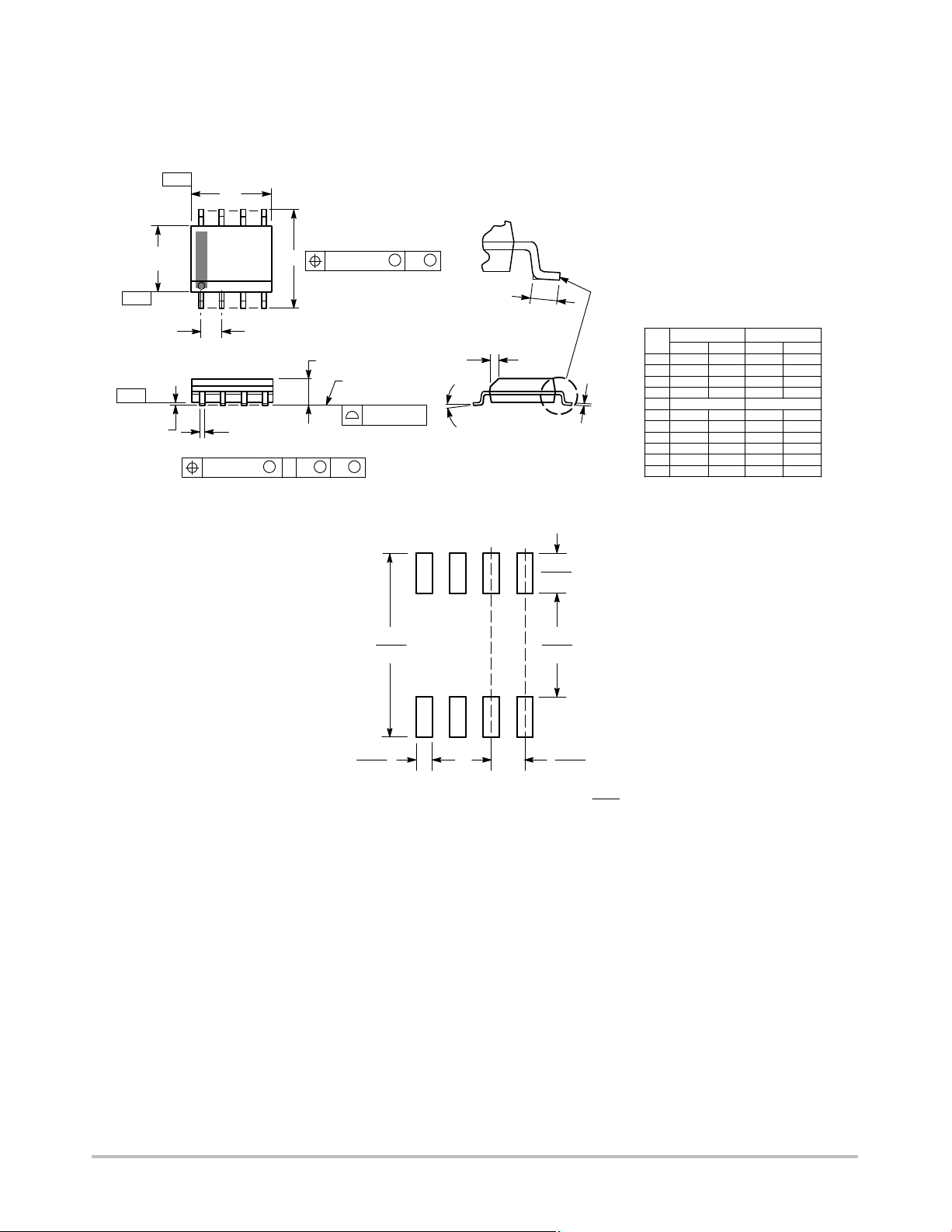
PACKAGE DIMENSIONS
SOIC−8 NB
CASE 751−07
ISSUE AH
−X−
B
H
A
58
1
4
G
D
0.25 (0.010) Z
M
S
Y
SXS
0.25 (0.010)
C
SEATING
PLANE
M
0.10 (0.004)
M
Y
K
N
X 45
_
M
J
NOTES:
1. DIMENSIONING AND TOLERANCING PER
ANSI Y14.5M, 1982.
2. CONTROLLING DIMENSION: MILLIMETER.
3. DIMENSION A AND B DO NOT INCLUDE
MOLD PROTRUSION.
4. MAXIMUM MOLD PROTRUSION 0.15 (0.006)
PER SIDE.
5. DIMENSION D DOES NOT INCLUDE DAMBAR
PROTRUSION. ALLOWABLE DAMBAR
PROTRUSION SHALL BE 0.127 (0.005) TOTAL
IN EXCESS OF THE D DIMENSION AT
MAXIMUM MATERIAL CONDITION.
6. 751−01 THRU 751−06 ARE OBSOLETE. NEW
STANDARD IS 751−07.
MILLIMETERS
DIMAMIN MAX MIN MAX
4.80 5.00 0.189 0.197
B 3.80 4.00 0.150 0.157
C 1.35 1.75 0.053 0.069
D 0.33 0.51 0.013 0.020
G 1.27 BSC 0.050 BSC
H 0.10 0.25 0.004 0.010
J 0.19 0.25 0.007 0.010
K 0.40 1.27 0.016 0.050
M 0 8 0 8
____
N 0.25 0.50 0.010 0.020
S 5.80 6.20 0.228 0.244
INCHES
SOLDERING FOOTPRINT*
1.52
0.060
7.0
0.275
0.6
0.024
*For additional information on our Pb−Free strategy and soldering
details, please download the ON Semiconductor Soldering and
Mounting Techniques Reference Manual, SOLDERRM/D.
4.0
0.155
1.270
0.050
SCALE 6:1
ǒ
inches
mm
Ǔ
http://onsemi.com
7

MC10EL51, MC100EL51
PACKAGE DIMENSIONS
TSSOP−8
DT SUFFIX
PLASTIC TSSOP PACKAGE
CASE 948R−02
ISSUE A
0.10 (0.004)
−T−
SEATING
PLANE
8x REFK
S
U0.15 (0.006) T
2X L/2
85
L
PIN 1
IDENT
S
U0.15 (0.006) T
0.10 (0.004) V
1
4
A
M
B
−U−
−V−
S
U
T
S
0.25 (0.010)
M
F
DETAIL E
C
D
G
DETAIL E
−W−
NOTES:
1. DIMENSIONING AND TOLERANCING PER ANSI
Y14.5M, 1982.
2. CONTROLLING DIMENSION: MILLIMETER.
3. DIMENSION A DOES NOT INCLUDE MOLD FLASH.
PROTRUSIONS OR GATE BURRS. MOLD FLASH
OR GATE BURRS SHALL NOT EXCEED 0.15
(0.006) PER SIDE.
4. DIMENSION B DOES NOT INCLUDE INTERLEAD
FLASH OR PROTRUSION. INTERLEAD FLASH OR
PROTRUSION SHALL NOT EXCEED 0.25 (0.010)
PER SIDE.
5. TERMINAL NUMBERS ARE SHOWN FOR
REFERENCE ONLY.
6. DIMENSION A AND B ARE TO BE DETERMINED
AT DATUM PLANE -W-.
DIM MIN MAX MIN MAX
A 2.90 3.10 0.114 0.122
B 2.90 3.10 0.114 0.122
C 0.80 1.10 0.031 0.043
D 0.05 0.15 0.002 0.006
F 0.40 0.70 0.016 0.028
G 0.65 BSC 0.026 BSC
K 0.25 0.40 0.010 0.016
L 4.90 BSC 0.193 BSC
M 0 6 0 6
____
INCHESMILLIMETERS
http://onsemi.com
8
MC10EL51, MC100EL51
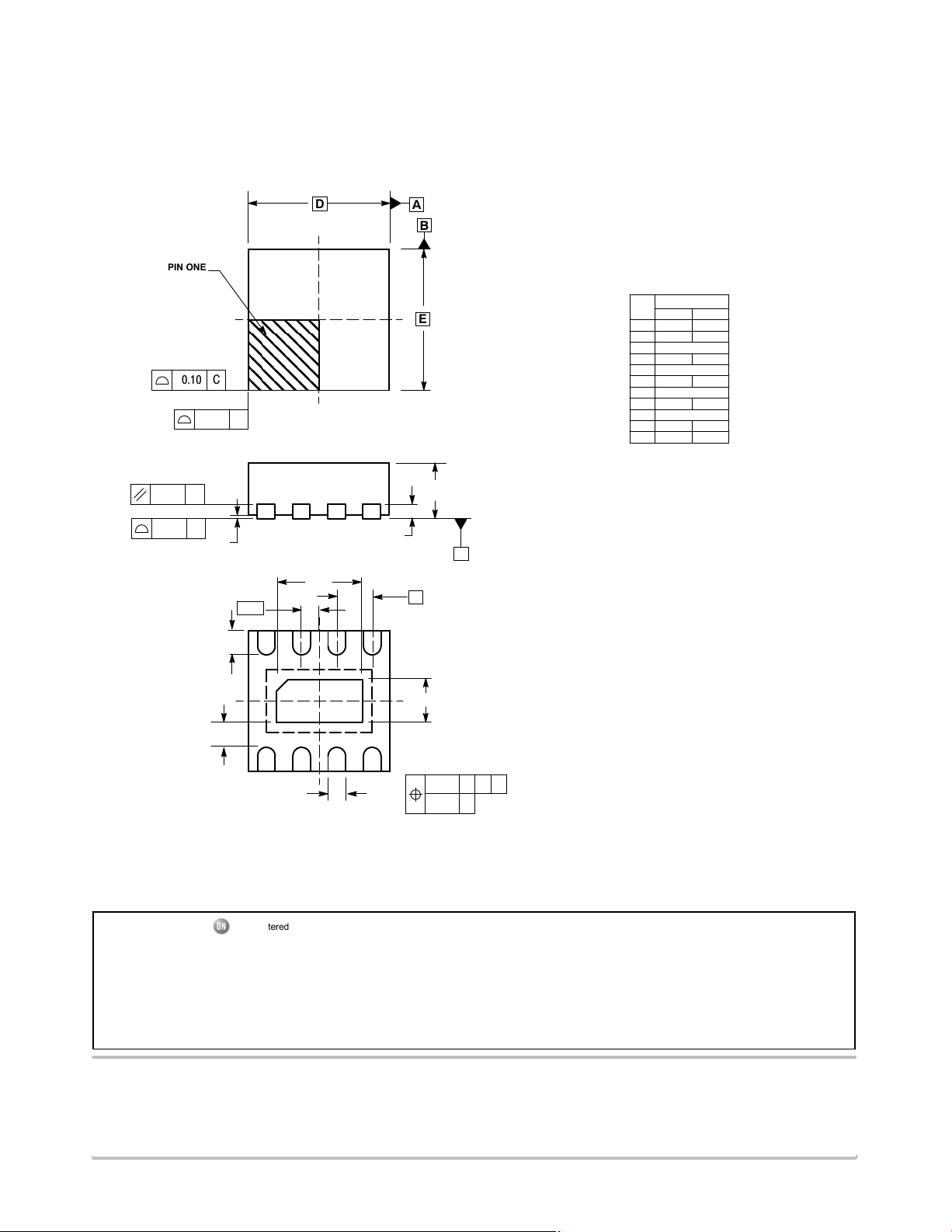
PACKAGE DIMENSIONS
DFN8
CASE 506AA−01
ISSUE D
8 X
REFERENCE
2 X
SEATING
PLANE
PIN ONE
2 X
C0.10
C0.08
C0.10
A1
8 X
D
A
B
E
C0.10
TOP VIEW
NOTES:
1. DIMENSIONING AND TOLERANCING PER
ASME Y14.5M, 1994 .
2. CONTROLLING DIMENSION: MILLIMETERS.
3. DIMENSION b APPLIES TO PLATED
TERMINAL AND IS MEASURED BETWEEN
0.25 AND 0.30 MM FROM TERMINAL.
4. COPLANARITY APPLIES TO THE EXPOSED
PAD AS WELL AS THE TERMINALS.
MILLIMETERS
DIM MIN MAX
A 0.80 1.00
A1 0.00 0.05
A3 0.20 REF
b 0.20 0.30
D 2.00 BSC
D2 1.10 1.30
E 2.00 BSC
E2 0.70 0.90
e 0.50 BSC
K 0.20 −−−
L 0.25 0.35
A
SIDE VIEW
(A3)
C
D2
e/2
1
e
4
L
E2
K
8
5
8 X
0.10 C
b
0.05 C
A
BB
NOTE 3
BOTTOM VIEW
ECLinPS is a trademark of Semiconductor Components INdustries, LLC (SCILLC).
ON Semiconductor and are registered trademarks of Semiconductor Components Industries, LLC (SCILLC). SCILLC reserves the right to make changes without further notice
to any products herein. SCILLC makes no warranty, representation or guarantee regarding the suitability of its products for any particular purpose, nor does SCILLC assume any liability
arising out of the application or use of any product or circuit, and specifically disclaims any and all liability, including without limitation special, consequential or incidental damages.
“Typical” parameters which may be provided in SCILLC data sheets and/or specifications can and do vary in different applications and actual performance may vary over time. All
operating parameters, including “Typicals” must be validated for each customer application by customer’s technical experts. SCILLC does not convey any license under its patent rights
nor the rights of others. SCILLC products are not designed, intended, or authorized for use as components in systems intended for surgical implant into the body, or other applications
intended to support or sustain life, or for any other application in which the failure of the SCILLC product could create a situation where personal injury or death may occur. Should
Buyer purchase or use SCILLC products for any such unintended or unauthorized application, Buyer shall indemnify and hold SCILLC and its officers, employees, subsidiaries, affiliates,
and distributors harmless against all claims, costs, damages, and expenses, and reasonable attorney fees arising out of, directly or indirectly, any claim of personal injury or death
associated with such unintended or unauthorized use, even if such claim alleges that SCILLC was negligent regarding the design or manufacture of the part. SCILLC is an Equal
Opportunity/Affirmative Action Employer. This literature is subject to all applicable copyright laws and is not for resale in any manner.
PUBLICATION ORDERING INFORMATION
LITERATURE FULFILLMENT:
Literature Distribution Center for ON Semiconductor
P.O. Box 5163, Denver, Colorado 80217 USA
Phone: 303−675−2175 or 800−344−3860 Toll Free USA/Canada
Fax: 303−675−2176 or 800−344−3867 Toll Free USA/Canada
Email: orderlit@onsemi.com
N. American Technical Support: 800−282−9855 Toll Free
USA/Canada
Europe, Middle East and Africa Technical Support:
Phone: 421 33 790 2910
Japan Customer Focus Center
Phone: 81−3−5773−3850
http://onsemi.com
ON Semiconductor Website: www.onsemi.com
Order Literature: http://www.onsemi.com/orderlit
For additional information, please contact your local
Sales Representative
MC10EL51/D
9
 Loading...