

Page 1
MC10186
查询"MC10186-D"供应商
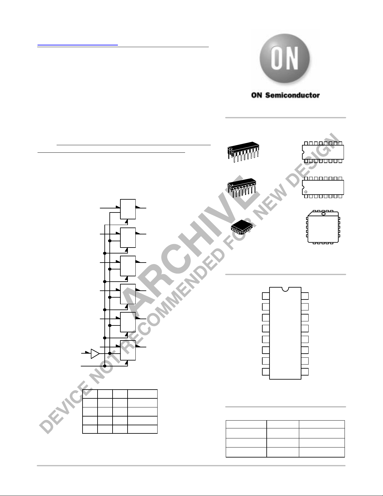
Hex D Master-Slave
Flip-Flop with Reset
The MC10186 contains six high–speed, master slave type “D”
flip–flops. Clocking is common to all six flip–flops. Data is entered
into the master when the clock is low. Master to slave data transfer
takes place on the positive–going Clock transition. Thus, outputs may
change only on a positive–going Clock transition. A change in the
information present at the data (D) input will not affect the output
information any other time due to the master–slave construction of this
device. A COMMON RESET IS INCLUDED IN THIS CIRCUIT.
RESET ONLY FUNCTIONS WHEN CLOCK IS LOW.
• P
= 460 mW typ/pkg (No Load)
D
• f
• t
= 150 MHz (typ)
toggle
, tf = 2.0 ns typ (20%–80%)
r
LOGIC DIAGRAM
D0
2 5
Q0
http://onsemi.com
16
CDIP–16
L SUFFIX
CASE 620
1
16
PDIP–16
P SUFFIX
CASE 648
1
MARKING
DIAGRAMS
MC10186L
AWLYYWW
MC10186P
AWLYYWW
1
CLOCK
RESET 1
6D1
7D2
10D3
11D4
12
D5
9
CLOCKED TRUTH TABLE
R C D Qn + 1
L L X Q
L H* L L
L H* H H
H L X L
*A clock H is a clock transition
from a low to a high state.
3 Q1
4 Q2
13 Q3
14 Q4
15 Q5
VCC= PIN 16
V
EE
n
= PIN 8
PLCC–20
FN SUFFIX
CASE 775
A = Assembly Location
WL = Wafer Lot
YY = Year
WW = Work Week
10186
AWLYYWW
DIP PIN ASSIGNMENT
RESET
Q0
Q1
Q2
D0
D1
D2
V
EE
Pin assignment is for Dual–in–Line Package.
For PLCC pin assignment, see the Pin Conversion Tables
on page 18 of the ON Semiconductor MECL Data Book
1
2
3
4
5
6
7
8
(DL122/D).
16
15
14
13
12
11
10
V
CC
Q5
Q4
Q3
D5
D4
D3
CLOCK
9
ORDERING INFORMATION
Device Package Shipping
MC10186L CDIP–16 25 Units / Rail
MC10186P PDIP–16 25 Units / Rail
MC10186FN PLCC–20 46 Units / Rail
Semiconductor Components Industries, LLC, 2002
January , 2002 – Rev. 7
1 Publication Order Number:
MC10186/D
Page 2
MC10186
Und
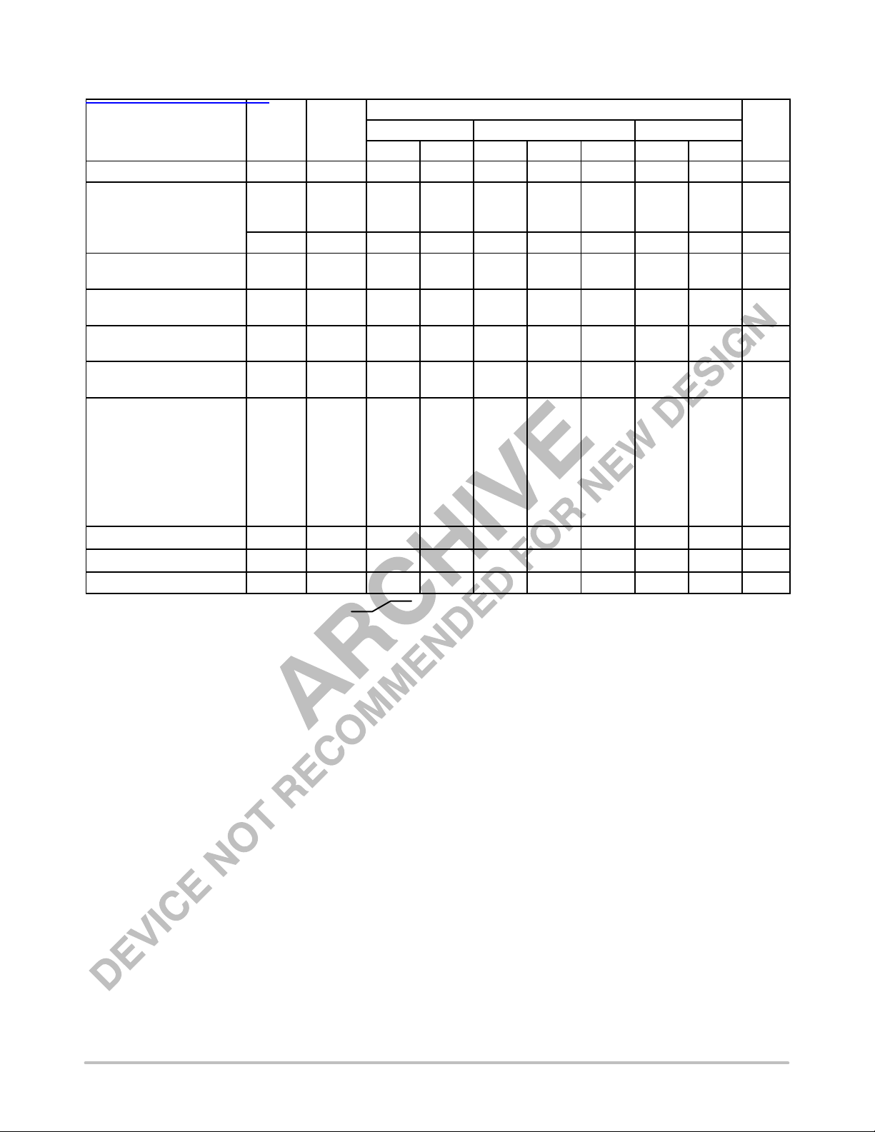
ELECTRICAL CHARACTERISTICS
查询"MC10186-D"供应商
Test Limits
Pin
er
Characteristic Symbol
Power Supply Drain Current I
Input Current I
E
inH
Test
8 121 88 110 121 mAdc
5
9
1
Output Voltage Logic 1 V
I
inL
OH
5 0.5 0.5 0.3 µAdc
2
15
Output Voltage Logic 0 V
OL
2
15
Threshold Voltage Logic 1 V
OHA
2
15
Threshold Voltage Logic 0 V
OLA
2
15
Switching Times (50Ω Load) ns
Propagation Delay t
Rise Time (20 to 80%) t
Fall Time (20 to 80%) t
Setup Time t
Hold Time t
Toggle Frequency (Max) f
1+3–
t
1+4–
t
9+2+
t
9+2–
setup
hold
tog
2+
2–
Output level to be measured after clock pulse.
3
4
2
2
2 1.0 4.1 1.1 1.8 4.0 1.1 4.4
2 1.0 4.1 1.1 1.8 4.0 1.1 4.4
2 2.5 2.5 2.5 2.5 ns
2 1.5 1.5 –1.5 1.5 ns
2 125 125 150 125 MHz
V
IL
–30°C +25°C +85°C
Min Max Min Typ Max Min Max
–1.060
–1.060
–1.890
–1.890
–1.080
–1.080
1.6
1.6
1.6
1.6
350
495
920
–0.890
–0.890
–1.675
–1.675
–0.960
–0.960
–1.850
–1.850
–0.980
–0.980
–1.655
–1.655
4.6
4.6
4.6
4.6
V
IH
appears at clock input (Pin 9).
1.6
1.6
1.6
1.6
2.5
2.5
3.5
3.5
220
310
575
–0.810
–0.810
–1.650
–1.650
–1.630
–1.630
4.5
4.5
4.5
4.5
–0.890
–0.890
–1.825
–1.825
–0.910
–0.910
1.6
1.6
1.6
1.6
–0.700
–0.700
–1.615
–1.615
–1.595
–1.595
220
310
575
5.0
5.0
5.0
5.0
Unit
µAdc
Vdc
Vdc
Vdc
Vdc
http://onsemi.com
2
Page 3
MC10186
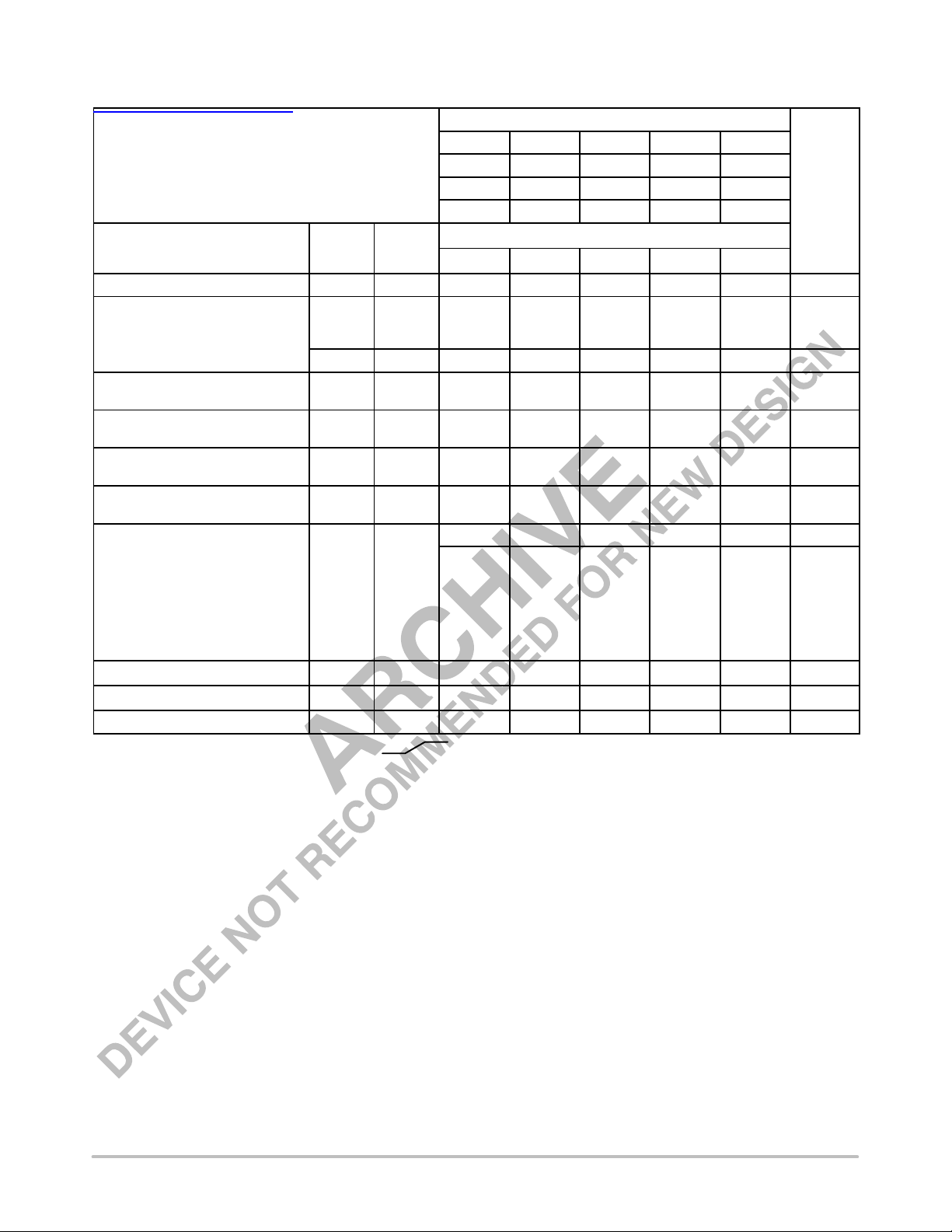
ELECTRICAL CHARACTERISTICS (continued)
查询"MC10186-D"供应商
TEST VOLTAGE VALUES (Volts)
@ Test Temperature V
IHmax
–30°C –0.890 –1.890 –1.205 –1.500 –5.2
+25°C –0.810 –1.850 –1.105 –1.475 –5.2
+85°C –0.700 –1.825 –1.035 –1.440 –5.2
Characteristic Symbol
Power Supply Drain Current I
Input Current I
Output Voltage Logic 1 V
Output Voltage Logic 0 V
Threshold Voltage Logic 1 V
Threshold Voltage Logic 0 V
E
inH
I
inL
OH
OL
OHA
OLA
Pin
Under
Test
8 8 16
5
9
1
5 5 8 16
2
15
2
15
2
15
2
15
TEST VOLTAGE APPLIED TO PINS LISTED BELOW
V
IHmax
5
9
1
5
12
Switching Times (50Ω Load) +1.11Vdc +0.31V Pulse In Pulse Out –3.2 V +2.0 V
Propagation Delay t
Rise Time (20 to 80%) t
Fall Time (20 to 80%) t
Setup Time t
Hold Time t
Toggle Frequency (Max) f
1+3–
t
1+4–
t
9+2+
t
9+2–
setup
hold
tog
2+
2–
Output level to be measured after clock pulse.
3
4
6
7
2
2
2 5, 9 2 8 16
2 5, 9 2 8 16
2 5, 9 2 8 16
2 5, 9 2 8 16
2 8 16
V
IH
V
IL
appears at clock input (Pin 9).
V
V
ILmin
ILmin
5
12
V
IHAmin
V
IHAmin
12
1, 9
1, 9
5, 9
5, 9
V
ILAmax
V
EE
(VCC)
V
ILAmax
V
EE
Gnd
8
8
8
8
8
8
8
5
8
8
5
12
3
4
2
2
8
8
8
8
8
8
16
16
16
16
16
16
16
16
16
16
16
16
16
16
16
Each MECL 10,000 series circuit has been designed to meet the dc specifications shown in the test table, after thermal equilibrium has been
established. The circuit is in a test socket or mounted on a printed circuit board and transverse air flow greater than 500 linear fpm is maintained.
Outputs are terminated through a 50–ohm resistor to –2.0 volts. Test procedures are shown for only one gate. The other gates are tested in the
same manner.
http://onsemi.com
3
Page 4

MC10186
查询"MC10186-D"供应商
–N–
–L–
20 1
V
A
Z
R
C
G
G1
0.010 (0.250) N
S
S
L-M
T
PACKAGE DIMENSIONS
PLASTIC PLCC PACKAGE
Y BRK
D
–M–
W
D
M
M
SEATING
PLANE
L-M
T
L-M
T
0.007 (0.180) N
0.007 (0.180) N
E
0.004 (0.100)
–T–
J
VIEW S
S
PLCC–20
FN SUFFIX
CASE 775–02
ISSUE C
M
0.007 (0.180) N
B
0.007 (0.180) N
U
Z
X
VIEW D–D
S
S
S
S
K1
NOTES:
1. DATUMS -L-, -M-, AND -N- DETERMINED
WHERE TOP OF LEAD SHOULDER EXITS PLASTIC
BODY AT MOLD PARTING LINE.
2. DIMENSION G1, TRUE POSITION TO BE
MEASURED AT DATUM -T-, SEATING PLANE.
3. DIMENSIONS R AND U DO NOT INCLUDE MOLD
FLASH. ALLOWABLE MOLD FLASH IS 0.010 (0.250)
PER SIDE.
4. DIMENSIONING AND TOLERANCING PER ANSI
Y14.5M, 1982.
5. CONTROLLING DIMENSION: INCH.
6. THE PACKAGE TOP MAY BE SMALLER THAN THE
PACKAGE BOTTOM BY UP TO 0.012 (0.300).
DIMENSIONS R AND U ARE DETERMINED AT THE
OUTERMOST EXTREMES OF THE PLASTIC BODY
EXCLUSIVE OF MOLD FLASH, TIE BAR BURRS,
GATE BURRS AND INTERLEAD FLASH, BUT
INCLUDING ANY MISMATCH BETWEEN THE TOP
AND BOTTOM OF THE PLASTIC BODY.
7. DIMENSION H DOES NOT INCLUDE DAMBAR
PROTRUSION OR INTRUSION. THE DAMBAR
PROTRUSION(S) SHALL NOT CAUSE THE H
DIMENSION TO BE GREATER THAN 0.037 (0.940).
THE DAMBAR INTRUSION(S) SHALL NOT CAUSE
THE H DIMENSION TO BE SMALLER THAN 0.025
(0.635).
L-M
T
M
K
VIEW S
S
S
S
T
G1
L-M
S
0.010 (0.250) N
0.007 (0.180) N
H
0.007 (0.180) N
F
DIM MIN MAX MIN MAX
A 0.385 0.395 9.78 10.03
B 0.385 0.395 9.78 10.03
C 0.165 0.180 4.20 4.57
E 0.090 0.110 2.29 2.79
F 0.013 0.019 0.33 0.48
G 0.050 BSC 1.27 BSC
H 0.026 0.032 0.66 0.81
J 0.020 --- 0.51 ---
K 0.025 --- 0.64 ---
R 0.350 0.356 8.89 9.04
U 0.350 0.356 8.89 9.04
V 0.042 0.048 1.07 1.21
W 0.042 0.048 1.07 1.21
X 0.042 0.056 1.07 1.42
Y --- 0.020 --- 0.50
Z 2 10 2 10
G1 0.310 0.330 7.88 8.38
K1 0.040 --- 1.02 ---
S
S
L-M
T
M
M
S
S
L-M
T
S
L-M
T
MILLIMETERSINCHES
S
S
http://onsemi.com
4
Page 5

MC10186
查询"MC10186-D"供应商
–A–
16 9
18
–T–
SEATING
PLANE
E
F
–A–
18
H
G
G
D
16 PL
0.25 (0.010) T
916
F
16 PL
D
N
M
A
B
C
S
K
0.25 (0.010) T
M
PACKAGE DIMENSIONS
CDIP–16
L SUFFIX
CERAMIC DIP PACKAGE
CASE 620–10
–B–
C
K
S
PLASTIC DIP PACKAGE
SEATING
–T–
PLANE
M
A
ISSUE T
L
16 PLJ
0.25 (0.010) T
PDIP–16
P SUFFIX
CASE 648–08
ISSUE R
L
J
NOTES:
1. DIMENSIONING AND TOLERANCING PER
ANSI Y14.5M, 1982.
2. CONTROLLING DIMENSION: INCH.
3. DIMENSION L TO CENTER OF LEAD WHEN
FORMED PARALLEL.
4. DIMENSION F MAY NARROW TO 0.76 (0.030)
WHERE THE LEAD ENTERS THE CERAMIC
BODY.
DIM MIN MAX MIN MAX
A 0.750 0.785 19.05 19.93
B 0.240 0.295 6.10 7.49
C --- 0.200 --- 5.08
D 0.015 0.020 0.39 0.50
E 0.050 BSC 1.27 BSC
F 0.055 0.065 1.40 1.65
M
M
S
B
NOTES:
1. DIMENSIONING AND TOLERANCING PER ANSI
2. CONTROLLING DIMENSION: INCH.
3. DIMENSION L TO CENTER OF LEADS WHEN
4. DIMENSION B DOES NOT INCLUDE MOLD FLASH.
5. ROUNDED CORNERS OPTIONAL.
M
G 0.100 BSC 2.54 BSC
H 0.008 0.015 0.21 0.38
K 0.125 0.170 3.18 4.31
L 0.300 BSC 7.62 BSC
M 0 15 0 15
N 0.020 0.040 0.51 1.01
Y14.5M, 1982.
FORMED PARALLEL.
DIM MIN MAX MIN MAX
A 0.740 0.770 18.80 19.55
B 0.250 0.270 6.35 6.85
C 0.145 0.175 3.69 4.44
D 0.015 0.021 0.39 0.53
F 0.040 0.70 1.02 1.77
G 0.100 BSC 2.54 BSC
H 0.050 BSC 1.27 BSC
J 0.008 0.015 0.21 0.38
K 0.110 0.130 2.80 3.30
L 0.295 0.305 7.50 7.74
M 0 10 0 10
S 0.020 0.040 0.51 1.01
MILLIMETERSINCHES
MILLIMETERSINCHES
http://onsemi.com
5
Page 6

Notes
查询"MC10186-D"供应商
MC10186
http://onsemi.com
6
Page 7

Notes
查询"MC10186-D"供应商
MC10186
http://onsemi.com
7
Page 8

查询"MC10186-D"供应商
MC10186
ON Semiconductor and are trademarks of Semiconductor Components Industries, LLC (SCILLC). SCILLC reserves the right to make changes
without further notice to any products herein. SCILLC makes no warranty, representation or guarantee regarding the suitability of its products for any particular
purpose, nor does SCILLC assume any liability arising out of the application or use of any product or circuit, and specifically disclaims any and all liability,
including without limitation special, consequential or incidental damages. “Typical” parameters which may be provided in SCILLC data sheets and/or
specifications can and do vary in different applications and actual performance may vary over time. All operating parameters, including “Typicals” must be
validated for each customer application by customer’s technical experts. SCILLC does not convey any license under its patent rights nor the rights of others.
SCILLC products are not designed, intended, or authorized for use as components in systems intended for surgical implant into the body, or other applications
intended to support or sustain life, or for any other application in which the failure of the SCILLC product could create a situation where personal injury or
death may occur. Should Buyer purchase or use SCILLC products for any such unintended or unauthorized application, Buyer shall indemnify and hold
SCILLC and its officers, employees, subsidiaries, affiliates, and distributors harmless against all claims, costs, damages, and expenses, and reasonable
attorney fees arising out of, directly or indirectly, any claim of personal injury or death associated with such unintended or unauthorized use, even if such claim
alleges that SCILLC was negligent regarding the design or manufacture of the part. SCILLC is an Equal Opportunity/Affirmative Action Employer.
PUBLICATION ORDERING INFORMATION
Literature Fulfillment:
Literature Distribution Center for ON Semiconductor
P.O. Box 5163, Denver, Colorado 80217 USA
Phone: 303–675–2175 or 800–344–3860 Toll Free USA/Canada
Fax: 303–675–2176 or 800–344–3867 Toll Free USA/Canada
Email: ONlit@hibbertco.com
N. American Technical Support: 800–282–9855 Toll Free USA/Canada
http://onsemi.com
JAPAN: ON Semiconductor, Japan Customer Focus Center
4–32–1 Nishi–Gotanda, Shinagawa–ku, Tokyo, Japan 141–0031
Phone: 81–3–5740–2700
Email: r14525@onsemi.com
ON Semiconductor Website: http://onsemi.com
For additional information, please contact your local
Sales Representative.
MC10186/D
8
 Loading...