

Page 1
MC100LVEP111
2.5V / 3.3V 1:10 Differential
ECL/PECL/HSTL Clock Driver
Description
The MC100LVEP111 is a low skew 1-to-10 differential driver,
designed with clock distribution in mind, accepting two clock sources into
an input multiplexer. The PECL input signals can be either differential or
single-ended (if the VBB output is used). HSTL inputs can be used when
the LVEP111 is operating under PECL conditions.
The LVEP111 specifically guarantees low output-to-output skew.
Optimal design, layout, and processing minimize skew within a device and
from device to device.
To ensure tightest skew, both sides of differential outputs identically
terminate into 50 W even if only one output is being used. If an output
pair is unused, both outputs may be left open (unterminated) without
affecting skew.
The MC100LVEP111, as with most other ECL devices, can be
operated from a positive VCC supply in PECL mode. This allows the
LVEP111 to be used for high performance clock distribution in +3.3 V or
+2.5 V systems. Single-ended CLK input operation is limited to a VCC ≥
3.0 V in PECL mode, or VEE v -3.0 V in NECL mode. Designers can
take advantage of the LVEP111's performance to distribute low skew
clocks across the backplane or the board. In a PECL environment, series
or Thevenin line terminations are typically used as they require no
additional power supplies. For more information on using PECL,
designers should refer to Application Note AN1406/D.
Features
•85 ps Typical Device-to-Device Skew
•20 ps Typical Output-to-Output Skew
•Jitter Less than 1 ps RMS
•Maximum Frequency > 3 GHz Typical
•V
Output
BB
•430 ps Typical Propagation Delay
•The 100 Series Contains Temperature Compensation
•PECL and HSTL Mode Operating Range: V
with VEE = 0 V
•NECL Mode Operating Range: V
CC
= 0 V
with VEE = -2.375 V to -3.8 V
•Open Input Default State
•LVDS Input Compatible
•Fully Compatible with MC100EP111
•Pb-Free Packages are Available
= 2.375 V to 3.8 V
CC
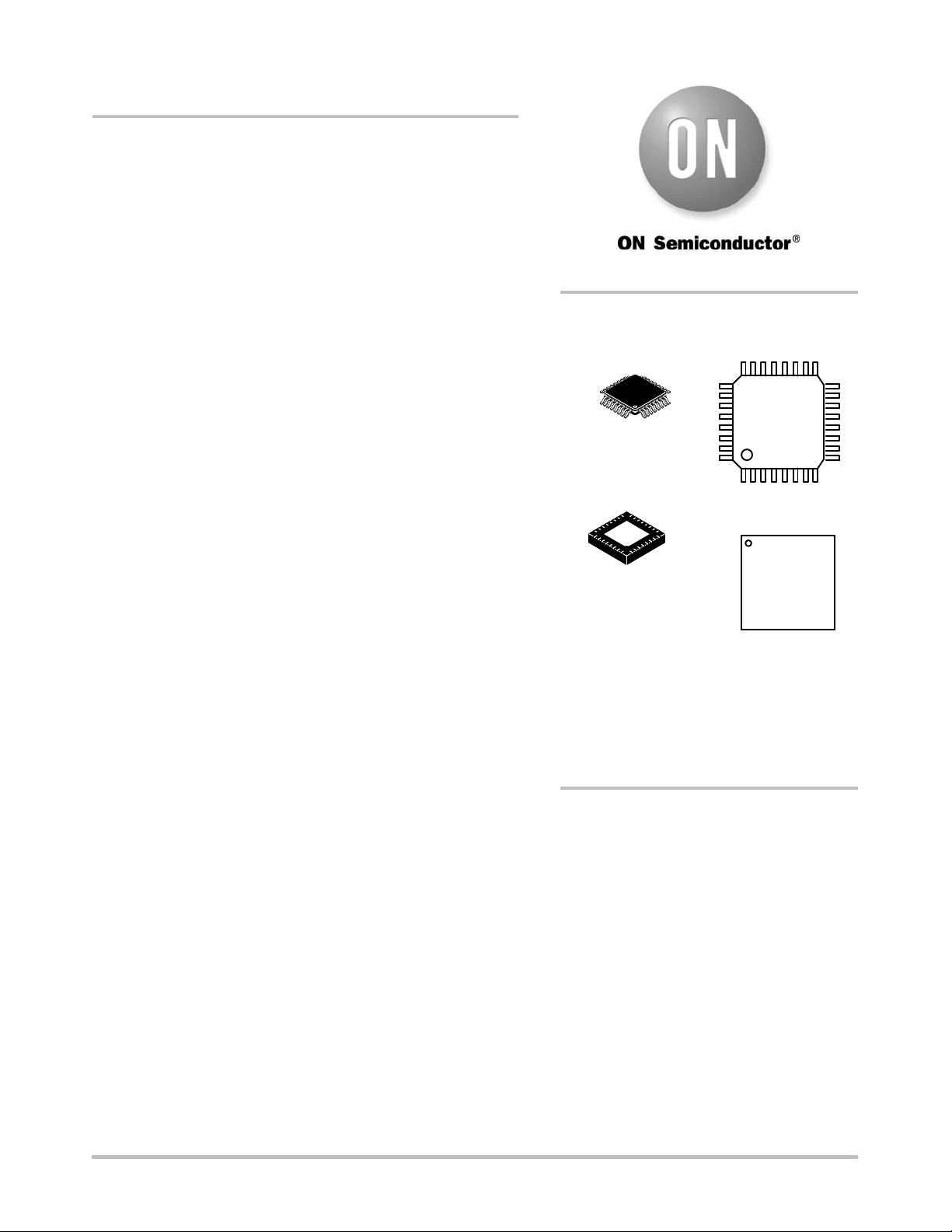
http://onsemi.com
MARKING
DIAGRAM*
MC100
LVEP111
AWLYYWWG
LQFP-32
FA SUFFIX
CASE 873A
32
1
QFN32
MN SUFFIX
CASE 488AM
A = Assembly Location
WL, L = Wafer Lot
YY, Y = Year
WW, W = Work Week
G = Pb-Free Package
*For additional marking information, refer to
Application Note AND8002/D.
See detailed ordering and shipping information in the package
dimensions section on page 9 of this data sheet.
ORDERING INFORMATION
32
1
1
MC100
LVEP111
ALYWG
© Semiconductor Components Industries, LLC, 2007
October, 2007 - Rev. 14
1 Publication Order Number:
MC100LVEP111/D
Page 2
MC100LVEP111
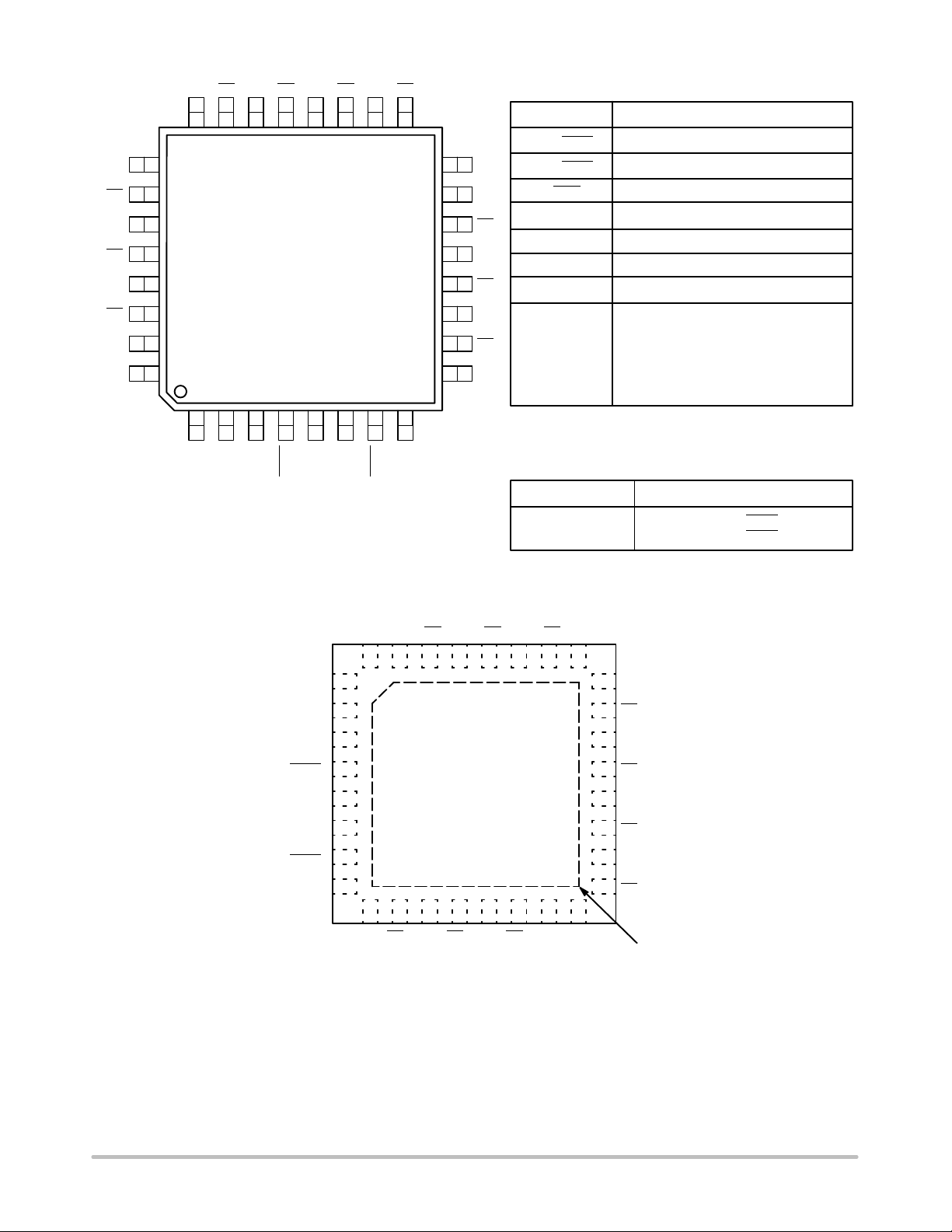
24 23 22 21 20 19 18 17
V
CC
Q2
Q2
Q1
25
26
27
28
MC100LVEP111
Q1
Q0
Q0
V
CC
29
30
31
32
12345678
CLK0
V
CLK0
BB
CLK1
CLK1
V
CC
CLK_SEL
Warning: All VCC and VEE pins must be externally connected
to Power Supply to guarantee proper operation.
Q6Q6Q5Q5Q4Q4Q3 Q3
16
15
14
13
12
11
10
9
Table 1. PIN DESCRIPTION
PIN
CLK0*, CLK0**
V
CLK1*, CLK1**
CC
Q0:9, Q0:9
Q7
CLK_SEL*
Q7
V
CC
V
V
EP
BB
CC
EE
Q8
Q8
Q9
Q9
V
FUNCTION
ECL/PECL/HSTL CLK Input
ECL/PECL/HSTL CLK Input
ECL/PECL Outputs
ECL/PECL Active Clock Select Input
Reference Voltage Output
Positive Supply
Negative Supply
The exposed pad (EP) on the package
bottom must be attached to a heat-sink‐
ing conduit. The exposed pad may only
be electrically connected to VEE.
* Pins will default LOW when left open.
** Pins will default to 2/3VCC when left open.
V
EE
Table 2. FUNCTION TABLE
CLK_SEL
L
H
Active Input
CLK0, CLK0
CLK1, CLK1
Figure 1. LQFP-32 Pinout (Top View)
VCCQ0 Q0 Q1 Q1 Q2 Q2 V
V
1
CC
CLK_SEL
CLK0
CLK0
CLK1
CLK1
2
3
4
5
V
BB
6
7
8
V
EE
V
Q9 Q9 Q8 Q8 Q7 Q7 V
CC
Figure 2. QFN-32 Pinout (Top View)
MC100LVEP111
CC
2526272829303132
24
Q3
23
Q3
22
Q4
21
Q4
20
Q5
19
Q5
18
Q6
17
Q6
1514131211109
16
CC
Exposed Pad (EP)
http://onsemi.com
2
Page 3
MC100LVEP111
Table 3. ATTRIBUTES
Characteristics Value
Internal Input Pulldown Resistor
Internal Input Pullup Resistor
ESD Protection Human Body Model
Machine Model
Charged Device Model
Moisture Sensitivity (Note 1) Pb Pkgs Pb-Free Pkgs
LQFP
QFN
Level 2
Level 1
Flammability Rating Oxygen Index: 28 to 34 UL 94 V-0 @ 0.125 in
Transistor Count 602 Devices
Meets or exceeds JEDEC Spec EIA/JESD78 IC Latchup Test
1. For additional information, refer to Application Note AND8003/D.
75 kW
37.5 kW
> 2 kV
> 100 V
> 2 kV
Level 2
Level 1
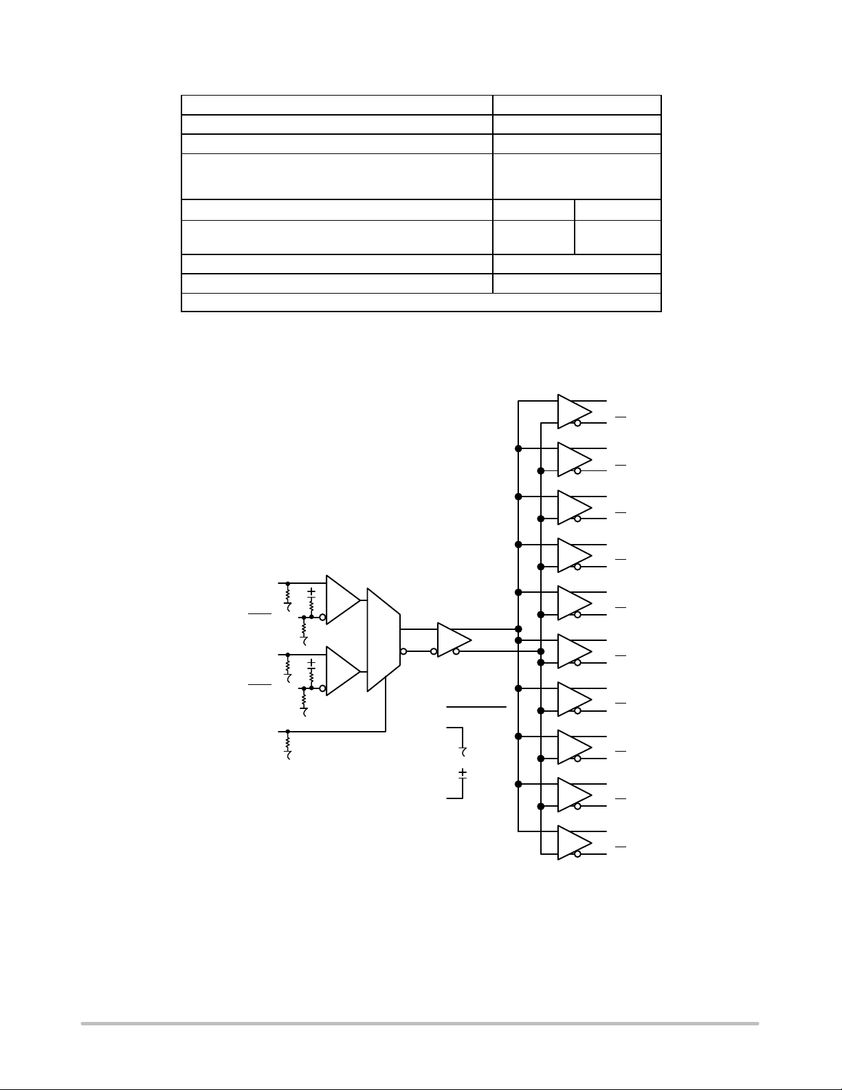
Q
0
Q
0
CLK0
CLK0
CLK1
CLK1
CLK_SEL
Q
1
Q
1
Q
2
Q
2
Q
3
Q
3
Q
0
1
V
BB
V
EE
V
CC
4
Q
4
Q
5
Q
5
Q
6
Q
6
Q
7
Q
7
Q
8
Q
8
Q
9
Q
9
Figure 3. Logic Diagram
http://onsemi.com
3
Page 4

MC100LVEP111
Table 4. MAXIMUM RATINGS
Symbol Parameter Condition 1 Condition 2 Rating Unit
V
CC
V
EE
V
I
I
out
I
BB
T
A
T
stg
q
JA
q
JC
q
JA
q
JC
T
sol
Stresses exceeding Maximum Ratings may damage the device. Maximum Ratings are stress ratings only. Functional operation above the
Recommended Operating Conditions is not implied. Extended exposure to stresses above the Recommended Operating Conditions may affect
device reliability.
PECL Mode Power Supply VEE = 0 V 6 V
NECL Mode Power Supply VCC = 0 V -6 V
PECL Mode Input Voltage
NECL Mode Input Voltage
Output Current Continuous
VEE = 0 V
VCC = 0 V
Surge
VI ≤ V
VI ≥ V
CC
EE
6
-6
50
100
V
V
mA
mA
VBB Sink/Source ± 0.5 mA
Operating Temperature Range -40 to +85 °C
Storage Temperature Range -65 to +150 °C
Thermal Resistance (Junction-to-Ambient) 0 lfpm
500 lfpm
LQFP-32
LQFP-32
80
55
°C/W
°C/W
Thermal Resistance (Junction-to-Case) Standard Board LQFP-32 12 to 17 °C/W
Thermal Resistance (Junction-to-Ambient) 0 lfpm
500 lfpm
QFN-32
QFN-32
31
27
°C/W
°C/W
Thermal Resistance (Junction-to-Case) 2S2P QFN-32 12 °C/W
Wave Solder Pb
Pb-Free (QFN-32 Only)
< 3 sec @ 248°C
< 3 sec @ 260°C
265
265
°C
http://onsemi.com
4
Page 5
MC100LVEP111
Table 5. PECL DC CHARACTERISTICS V
= 2.5 V; V
CC
= 0 V (Note 2)
EE
-40°C 25°C 85°C
Symbol Characteristic Min Typ Max Min Typ Max Min Typ Max Unit
I
EE
V
OH
V
OL
V
IH
V
IL
V
IHCMR
Power Supply Current 60 90 120 60 90 120 60 90 120 mA
Output HIGH Voltage (Note 3) 1355 1480 1605 1355 1480 1605 1355 1480 1605 mV
Output LOW Voltage (Note 3) 555 730 900 555 730 900 555 730 900 mV
Input HIGH Voltage (Single-Ended)
1335 1620 1335 1620 1275 1620 mV
(Note 4)
Input LOW Voltage (Single-Ended)
555 875 555 875 555 875 mV
(Note 4)
Input HIGH Voltage Common Mode
1.2 2.5 1.2 2.5 1.2 2.5 V
Range (Differential Configuration)
(Note 5)
I
IH
I
IL
Input HIGH Current 150 150 150
Input LOW Current CLK
CLK
0.5
-150
0.5
-150
0.5
-150
mA
mA
NOTE: Device will meet the specifications after thermal equilibrium has been established when mounted in a test socket or printed circuit
board with maintained transverse airflow greater than 500 lfpm. Electrical parameters are guaranteed only over the declared
operating temperature range. Functional operation of the device exceeding these conditions is not implied. Device specification limit
values are applied individually under normal operating conditions and not valid simultaneously.
2. Input and output parameters vary 1:1 with VCC. VEE can vary + 0.125 V to -1.3 V.
3. All loading with 50 W to VEE.
4. Do not use VBB at VCC < 3.0 V.
5. V
min varies 1:1 with VEE, V
IHCMR
input signal.
max varies 1:1 with VCC. The V
IHCMR
range is referenced to the most positive side of the differential
IHCMR
Table 6. PECL DC CHARACTERISTICS V
= 3.3 V; V
CC
= 0 V (Note 6)
EE
-40°C 25°C 85°C
Symbol Characteristic Min Typ Max Min Typ Max Min Typ Max Unit
I
EE
V
OH
V
OL
V
IH
V
IL
V
BB
V
IHCMR
Power Supply Current 60 90 120 60 90 120 60 90 120 mA
Output HIGH Voltage (Note 7) 2155 2280 2405 2155 2280 2405 2155 2280 2405 mV
Output LOW Voltage (Note 7) 1355 1530 1700 1355 1530 1700 1355 1530 1700 mV
Input HIGH Voltage (Single-Ended) 2135 2420 2135 2420 2135 2420 mV
Input LOW Voltage (Single-Ended) 1355 1675 1355 1675 1355 1675 mV
Output Reference Voltage (Note 8) 1775 1875 1975 1775 1875 1975 1775 1875 1975 mV
Input HIGH Voltage Common Mode
1.2 3.3 1.2 3.3 1.2 3.3 V
Range (Differential Configuration)
(Note 9)
I
IH
I
IL
Input HIGH Current 150 150 150
Input LOW Current CLK
CLK
0.5
-150
0.5
-150
0.5
-150
mA
mA
NOTE: Device will meet the specifications after thermal equilibrium has been established when mounted in a test socket or printed circuit
board with maintained transverse airflow greater than 500 lfpm. Electrical parameters are guaranteed only over the declared
operating temperature range. Functional operation of the device exceeding these conditions is not implied. Device specification limit
values are applied individually under normal operating conditions and not valid simultaneously.
6. Input and output parameters vary 1:1 with VCC. VEE can vary + 0.925 V to -0.5 V.
7. All loading with 50 W to VCC - 2.0 V.
8. Single ended input operation is limited VCC ≥ 3.0 V in PECL mode.
9. V
min varies 1:1 with VEE, V
IHCMR
input signal.
max varies 1:1 with VCC. The V
IHCMR
range is referenced to the most positive side of the differential
IHCMR
http://onsemi.com
5
Page 6
MC100LVEP111
Table 7. NECL DC CHARACTERISTICS V
= 0 V, V
CC
= -2.375 V to -3.8 V (Note 10)
EE
-40°C 25°C 85°C
Symbol Characteristic Min Ty p Max Min Typ Max Min Typ Max Unit
I
EE
V
OH
V
OL
V
IH
V
IL
V
BB
V
IHCMR
Power Supply Current 60 90 120 60 90 120 60 90 120 mA
Output HIGH Voltage (Note 11) -1145 -1020 -895 -1145 -1020 -895 -1145 -1020 -895 mV
Output LOW Voltage (Note 11) -1945 -1770 -1600 -1945 -1770 -1600 -1945 -1770 -1600 mV
Input HIGH Voltage (Single-Ended) -1165 -880 -1165 -880 -1165 -880 mV
Input LOW Voltage (Single-Ended) -1945 -1625 -1945 -1625 -1945 -1625 mV
Output Reference Voltage (Note 12) -1525 -1425 -1325 -1525 -1425 -1325 -1525 -1425 -1325 mV
Input HIGH Voltage Common Mode
VEE + 1.2 0.0 VEE + 1.2 0.0 VEE + 1.2 0.0 V
Range (Differential Configuration)
(Note 13)
I
IH
I
IL
Input HIGH Current 150 150 150
Input LOW Current CLK
CLK
0.5
-150
0.5
-150
0.5
-150
mA
mA
NOTE: Device will meet the specifications after thermal equilibrium has been established when mounted in a test socket or printed circuit
board with maintained transverse airflow greater than 500 lfpm. Electrical parameters are guaranteed only over the declared
operating temperature range. Functional operation of the device exceeding these conditions is not implied. Device specification limit
values are applied individually under normal operating conditions and not valid simultaneously.
10.Input and output parameters vary 1:1 with VCC.
11.All loading with 50 W to VCC - 2.0 V.
12.Single ended input operation is limited VEE ≤ -3.0V in NECL mode.
13.V
min varies 1:1 with VEE, V
IHCMR
input signal.
max varies 1:1 with VCC. The V
IHCMR
range is referenced to the most positive side of the differential
IHCMR
Table 8. HSTL DC CHARACTERISTICS V
= 2.375 to 3.8 V, VEE = 0 V
CC
-40°C 25°C 85°C
Symbol Characteristic Min Typ Max Min Typ Max Min Typ Max Unit
V
IH
V
IL
Input HIGH Voltage 1200 1200 1200 mV
Input LOW Voltage 400 400 400 mV
Vx Input Crossover Voltage 680 900 680 900 680 900 mV
I
CC
Power Supply Current 70 100 120 70 100 120 70 100 120 mA
NOTE: Device will meet the specifications after thermal equilibrium has been established when mounted in a test socket or printed circuit
board with maintained transverse airflow greater than 500 lfpm. Electrical parameters are guaranteed only over the declared
operating temperature range. Functional operation of the device exceeding these conditions is not implied. Device specification limit
values are applied individually under normal operating conditions and not valid simultaneously.
http://onsemi.com
6
Page 7
MC100LVEP111
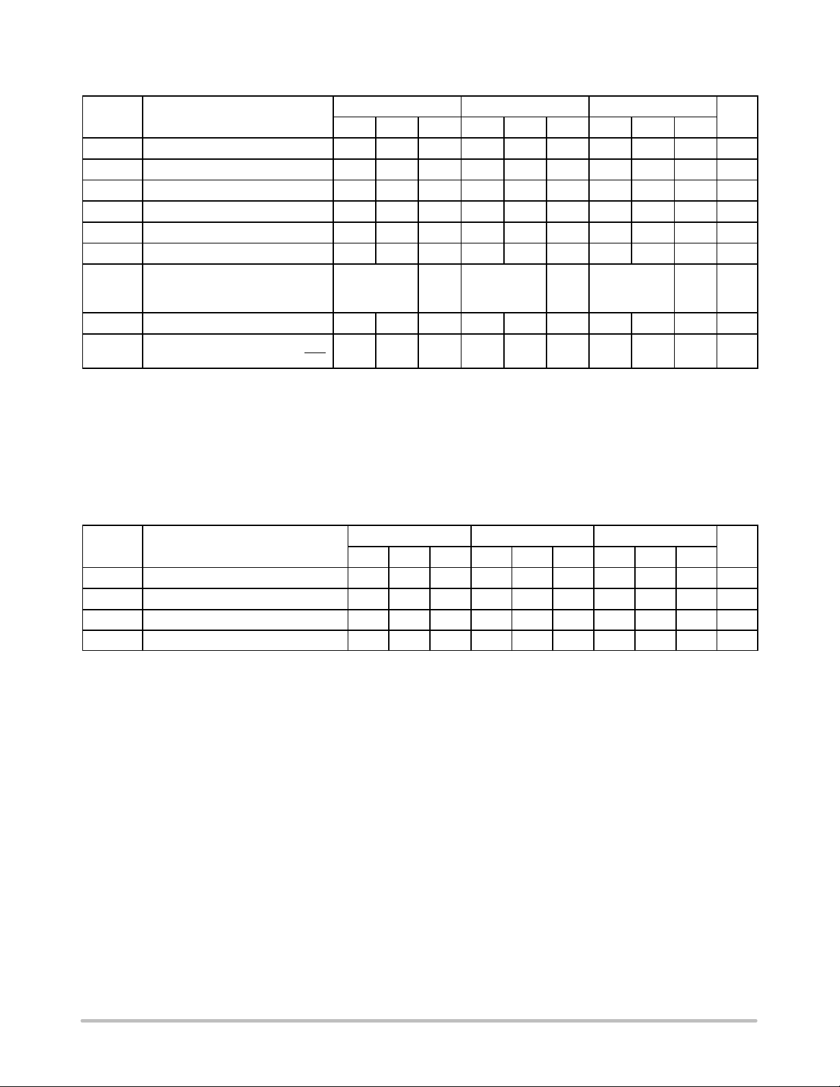
Table 9. AC CHARACTERISTICS V
= 0 V; VEE = -2.375 to -3.8 V or VCC = 2.375 to 3.8 V; VEE = 0 V (Note 14)
CC
-40°C 25°C 85°C
Symbol
f
maxPECL/HSTL
t
PLH
t
PHL
t
skew
t
JITTER
V
PP
tr/t
f
Maximum Frequency (Figure 4) 3 3 3 GHz
Propagation Delay
(Differential Configuration)
Within-Device Skew (Note 15)
Within-Device Skew @ 2.5 V (Note 15)
Device-to-Device Skew (Note 16)
CLOCK Random Jitter (RMS)
@ v0.5 GHz
@ v1.0 GHz
@ v1.5 GHz
@ v2.0 GHz
@ v2.5 GHz
@ v3.0 GHz
Input Swing (Differential Interconnect
Configuration) Measured Single-Ended
Output Rise/Fall Time (20%-80%) 105 200 255 125 200 275 150 230 320 ps
Characteristic Min Typ Max Min Ty p Max Min Typ Max
325 400 475 350 430 500 440 510 590 ps
20
20
85
0.209
0.200
0.197
0.220
0.232
0.348
25
25
150
0.5
0.5
0.4
0.5
0.4
0.6
20
20
85
0.204
0.214
0.213
0.224
0.290
0.545
25
25
150
0.5
0.6
0.5
0.5
0.5
0.8
25
20
85
0.221
0.229
0.243
0.292
0.522
0.911
35
25
150
0.5
0.5
0.4
0.6
0.8
1.3
150 800 1200 150 800 1200 150 800 1200 mV
Unit
ps
ps
NOTE: Device will meet the specifications after thermal equilibrium has been established when mounted in a test socket or printed circuit
board with maintained transverse airflow greater than 500 lfpm. Electrical parameters are guaranteed only over the declared
operating temperature range. Functional operation of the device exceeding these conditions is not implied. Device specification limit
values are applied individually under normal operating conditions and not valid simultaneously.
14.Measured with 750 mV source, 50% duty cycle clock source. All loading with 50 W to VCC - 2.0 V.
15.Skew is measured between outputs under identical transitions and conditions on any one device.
16.Device-to-Device skew for identical transitions at identical VCC levels.
800
700
600
(mV)
500
OUTpp
V
400
300
200
100
0
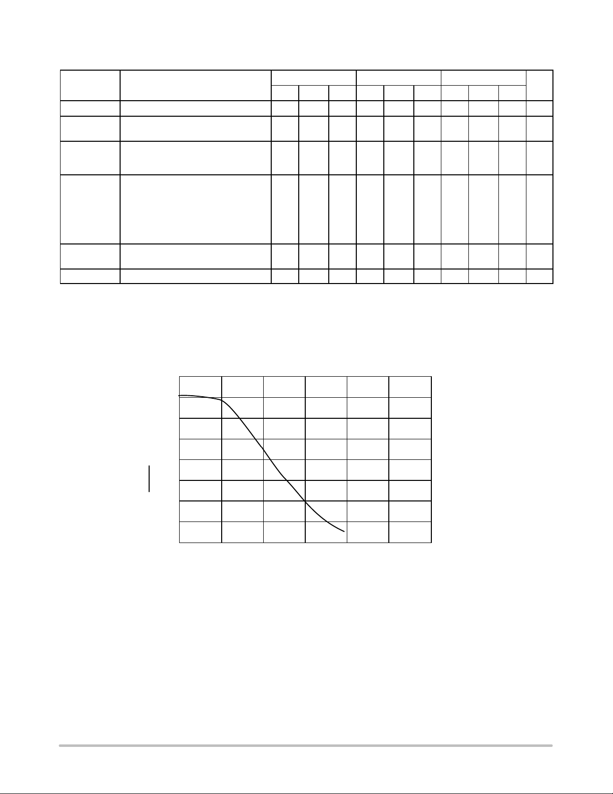
0 1000 2000 3000 4000 5000 6000
FREQUENCY (MHz)
Figure 4. F
max
Typical
http://onsemi.com
7
Page 8
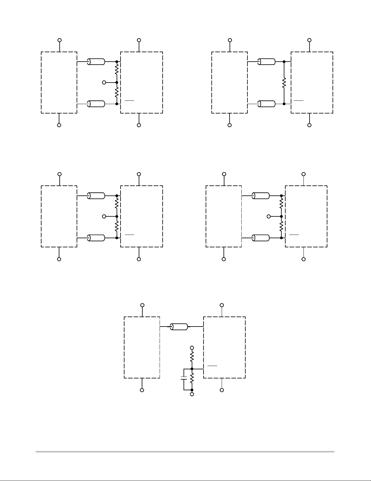
MC100LVEP111
V
CC
Z0 = 50 W
50 W
LVPECL
Driver
V
TT
50 W
Z0 = 50 W
VT = VCC - 2.0 V
V
EE
Figure 5. LVPECL in Interface
V
CC
Z0 = 50 W
50 W
HSTL
Driver
V
DDQ
50 W
Z0 = 50 W
V
CC
MC100LVEP111 MC100LVEP111
CLKx
V
CC
V
CC
Z0 = 50 W
CLKx
50 W*
CLK
LVDS
Driver
V
EE
GND GND
100 W
Z0 = 50 W
50 W*
CLK
Figure 6. LVDS in Interface
V
CC
MC100LVEP111
CLKx
CLK
V
CC
CML
Driver
Z0 = 50 W
V
CC
Z0 = 50 W
50 W
50 W
V
CC
MC100LVEP111
CLKx
CLK
V
EE
Figure 7. HSTL in Interface
Figure 9. Single-Ended Interface LVCMOS/LVTTL in Interface
V
EE
V
CC
LVCMOS
LVTTL
Single-Ended
Driver
V
EE
Z0 = 50 W
V
CC
GND
V
EE
Figure 8. Standard 50 W Load CML in Interface
V
CC
MC100LVEP111
CLKx
1k
CLK
1k
V
EE
V
EE
http://onsemi.com
8
Page 9

MC100LVEP111
Zo = 50 W
Zo = 50 W
50 W 50 W
V
VTT = VCC - 2.0 V
TT
Receiver
Device
Driver
Device
QD
Q D
Figure 10. Typical Termination for Output Driver and Device Evaluation
(See Application Note AND8020/D - Termination of ECL Logic Devices.)
ORDERING INFORMATION
Device Package Shipping
MC100LVEP111FA LQFP-32 250 Units / Tray
MC100LVEP111FAG LQFP-32
(Pb-Free)
MC100LVEP111FAR2 LQFP-32 2000 / Tape & Reel
MC100LVEP111FARG LQFP-32
(Pb-Free)
MC100LVEP111MNG QFN-32
(Pb-Free)
MC100LVEP111MNRG QFN-32
(Pb-Free)
†For information on tape and reel specifications, including part orientation and tape sizes, please refer to our Tape and Reel Packaging
Specifications Brochure, BRD8011/D.
250 Units / Tray
2000 / Tape & Reel
74 Units / Rail
1000 / Tape & Reel
†
Resource Reference of Application Notes
AN1405/D - ECL Clock Distribution Techniques
AN1406/D - Designing with PECL (ECL at +5.0 V)
AN1503/D -
AN1504/D - Metastability and the ECLinPS Family
AN1568/D - Interfacing Between LVDS and ECL
AN1672/D - The ECL Translator Guide
AND8001/D - Odd Number Counters Design
AND8002/D - Marking and Date Codes
AND8020/D - Termination of ECL Logic Devices
AND8066/D - Interfacing with ECLinPS
AND8090/D - AC Characteristics of ECL Devices
ECLinPSt I/O SPiCE Modeling Kit
http://onsemi.com
9
Page 10

MC100LVEP111
PACKAGE DIMENSIONS
32 LEAD LQFP
CASE 873A-02
ISSUE C
SEATING
PLANE
9
-T-
B1
-AB-
-AC-
A
A1
32
1
4X
25
-U-
T-U0.20 (0.008) ZAB
P
-T-, -U-, -Z-
AE
VB
AE
DETAIL Y
8
9
-Z-
S1
V1
17
4X
T-U0.20 (0.008) ZAC
DETAIL Y
BASE
METAL
N
T-U
M
DF
S
_
M
8X
G
DETAIL AD
E
C
R
J
SECTION AE-AE
0.20 (0.008) ZAC
0.10 (0.004) AC
H
W
_
Q
K
X
DETAIL AD
NOTES:
1. DIMENSIONING AND TOLERANCING
PER ANSI Y14.5M, 1982.
2. CONTROLLING DIMENSION:
MILLIMETER.
3. DATUM PLANE -AB- IS LOCATED AT
BOTTOM OF LEAD AND IS COINCIDENT
WITH THE LEAD WHERE THE LEAD
EXITS THE PLASTIC BODY AT THE
BOTTOM OF THE PARTING LINE.
4. DATUMS -T-, -U-, AND -Z- TO BE
DETERMINED AT DATUM PLANE -AB-.
5. DIMENSIONS S AND V TO BE
DETERMINED AT SEATING PLANE -AC-.
6. DIMENSIONS A AND B DO NOT INCLUDE
MOLD PROTRUSION. ALLOWABLE
PROTRUSION IS 0.250 (0.010) PER SIDE.
DIMENSIONS A AND B DO INCLUDE
MOLD MISMATCH AND ARE
DETERMINED AT DATUM PLANE -AB-.
7. DIMENSION D DOES NOT INCLUDE
DAMBAR PROTRUSION. DAMBAR
PROTRUSION SHALL NOT CAUSE THE
D DIMENSION TO EXCEED 0.520 (0.020).
8. MINIMUM SOLDER PLATE THICKNESS
SHALL BE 0.0076 (0.0003).
9. EXACT SHAPE OF EACH CORNER MAY
VARY FROM DEPICTION.
0.250 (0.010)
GAUGE PLANE
MILLIMETERS
DIMAMIN MAX MIN MAX
7.000 BSC 0.276 BSC
A1 3.500 BSC 0.138 BSC
B 7.000 BSC 0.276 BSC
B1 3.500 BSC 0.138 BSC
C 1.400 1.600 0.055 0.063
D 0.300 0.450 0.012 0.018
E 1.350 1.450 0.053 0.057
F 0.300 0.400 0.012 0.016
G 0.800 BSC 0.031 BSC
H 0.050 0.150 0.002 0.006
J 0.090 0.200 0.004 0.008
K 0.450 0.750 0.018 0.030
__
M 12 REF 12 REF
N 0.090 0.160 0.004 0.006
P 0.400 BSC 0.016 BSC
Q 1 5 1 5
____
R 0.150 0.250 0.006 0.010
S 9.000 BSC 0.354 BSC
S1 4.500 BSC 0.177 BSC
V 9.000 BSC 0.354 BSC
V1 4.500 BSC 0.177 BSC
W 0.200 REF 0.008 REF
X 1.000 REF 0.039 REF
INCHES
http://onsemi.com
10
Page 11
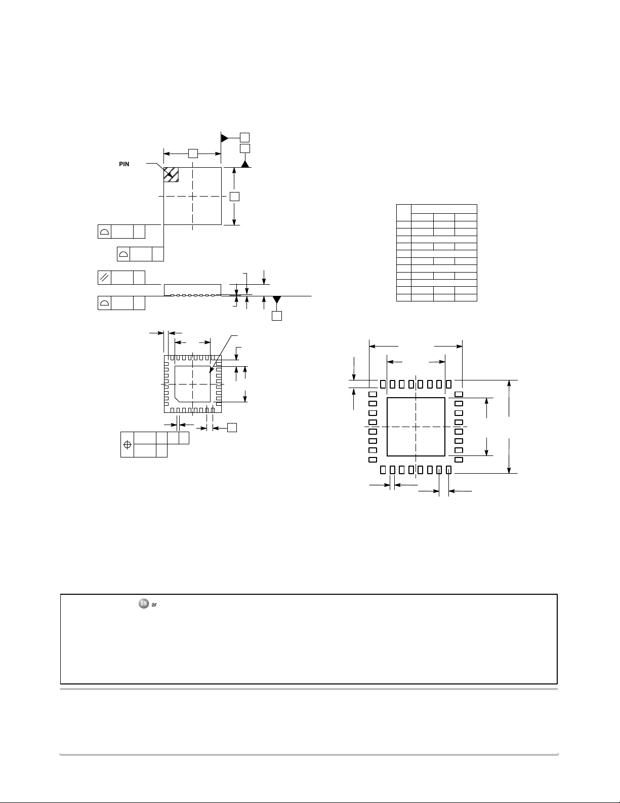
MC100LVEP111
PACKAGE DIMENSIONS
QFN32 5*5*1 0.5 P
CASE 488AM-01
ISSUE O
2 X
32 X
LOCATION
0.15 C
2 X
0.10 C
0.08 C
PIN ONE
0.15 C
32 X
L
32 X
0.05 C
TOP VIEW
SIDE VIEW
9
8
1
32
b
A0.10 BC
D
D2
(A3)
A1
16
17
24
25
A
B
E
EXPOSED PAD
K
32 X
E2
e
NOTES:
1. DIMENSIONS AND TOLERANCING PER
ASME Y14.5M, 1994.
2. CONTROLLING DIMENSION: MILLIMETERS.
3. DIMENSION b APPLIES TO PLATED
TERMINAL AND IS MEASURED BETWEEN
0.25 AND 0.30 MM TERMINAL
4. COPLANARITY APPLIES TO THE EXPOSED
PAD AS WELL AS THE TERMINALS.
MILLIMETERS
DIM MIN NOM MAX
A 0.800 0.900 1.000
A1 0.000 0.025 0.050
A3 0.200 REF
b 0.180 0.250 0.300
D 5.00 BSC
D2 2.950 3.100 3.250
E 5.00 BSC
E2
2.950 3.100 3.250
A
SEATING
PLANE
e 0.500 BSC
K 0.200 --- ---
L 0.300 0.400 0.500
C
SOLDERING FOOTPRINT*
5.30
3.20
32 X
0.63
3.20
5.30
BOTTOM VIEW
32 X
0.28
DIMENSIONS: MILLIMETERS
28 X
0.50 PITCH
*For additional information on our Pb-Free strategy and soldering
details, please download the ON Semiconductor Soldering and
Mounting Techniques Reference Manual, SOLDERRM/D.
ECLinPS is a trademark of Semiconductor Components Industries, LLC (SCILLC).
ON Semiconductor and are registered trademarks of Semiconductor Components Industries, LLC (SCILLC). SCILLC reserves the right to make changes without further notice
to any products herein. SCILLC makes no warranty, representation or guarantee regarding the suitability of its products for any particular purpose, nor does SCILLC assume any liability
arising out of the application or use of any product or circuit, and specifically disclaims any and all liability, including without limitation special, consequential or incidental damages.
“Typical” parameters which may be provided in SCILLC data sheets and/or specifications can and do vary in different applications and actual performance may vary over time. All
operating parameters, including “Typicals” must be validated for each customer application by customer's technical experts. SCILLC does not convey any license under its patent rights
nor the rights of others. SCILLC products are not designed, intended, or authorized for use as components in systems intended for surgical implant into the body, or other applications
intended to support or sustain life, or for any other application in which the failure of the SCILLC product could create a situation where personal injury or death may occur. Should
Buyer purchase or use SCILLC products for any such unintended or unauthorized application, Buyer shall indemnify and hold SCILLC and its officers, employees, subsidiaries, affiliates,
and distributors harmless against all claims, costs, damages, and expenses, and reasonable attorney fees arising out of, directly or indirectly, any claim of personal injury or death
associated with such unintended or unauthorized use, even if such claim alleges that SCILLC was negligent regarding the design or manufacture of the part. SCILLC is an Equal
Opportunity/Affirmative Action Employer. This literature is subject to all applicable copyright laws and is not for resale in any manner.
PUBLICATION ORDERING INFORMATION
LITERATURE FULFILLMENT:
Literature Distribution Center for ON Semiconductor
P.O. Box 5163, Denver, Colorado 80217 USA
Phone: 303-675-2175 or 800-344-3860 Toll Free USA/Canada
Fax: 303-675-2176 or 800-344-3867 Toll Free USA/Canada
Email: orderlit@onsemi.com
N. American Technical Support: 800-282-9855 Toll Free
USA/Canada
Japan: ON Semiconductor, Japan Customer Focus Center
2-9-1 Kamimeguro, Meguro-ku, Tokyo, Japan 153-0051
Phone: 81-3-5773-3850
http://onsemi.com
ON Semiconductor Website: http://onsemi.com
Order Literature: http://www.onsemi.com/litorder
For additional information, please contact your
local Sales Representative.
MC100LVEP111/D
11
 Loading...