

Page 1
3.3 V/5 V ECL 2-Input
Differential XOR/XNOR
MC10EP08, MC100EP08
Description
The MC10/100EP08 is a differential XOR/XNOR gate. The EP08 is
ideal for applications requiring the fastest AC performance available.
The 100 Series contains temperature compensation.
Features
• 250 ps Typical Propagation Delay
• Maximum Frequency = > 3 GHz Typical
• PECL Mode Operating Range:
= 3.0 V to 5.5 V with V
V
CC
• NECL Mode Operating Range:
= 0 V with V
V
CC
= −3.0 V to −5.5 V
EE
• Open Input Default State
• Safety Clamp on Inputs
• Q Output Will Default LOW with Inputs Open or at V
• These Devices are Pb-Free, Halogen Free and are RoHS Compliant
EE
= 0 V
EE
www.onsemi.com
8
1
SOIC−8 NB
D SUFFIX
CASE 751−07
8
1
TSSOP−8
DT SUFFIX
CASE 948R−02
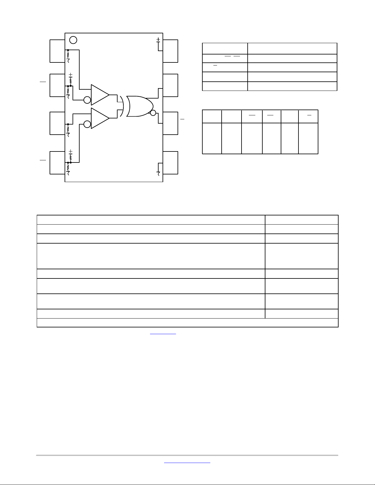
MARKING DIAGRAMS*
8
HEP08
ALYW
G
1
8
KEP01
ALYW
G
1
SOIC−8 NB TSSOP−8
8
HP08
ALYWG
G
1
8
KP082
ALYWG
G
1
A = Assembly Location
L = Wafer Lot
H = MC10
K = MC100
(Note: Microdot may be in either location)
*For additional marking information, refer to
Application Note AND8002/D
Y = Year
W = Work Week
G = Pb-Free Package
.
ORDERING INFORMATION
Device
MC10EP08DG
MC10EP08DR2G
MC10EP08DTG
MC100EP08DG
MC100EP08DTG
MC100EP08DTR2G
†For information on tape and reel specifications,
including part orientation and tape sizes, please
refer to our Tape and Reel Packaging Specifications Brochure, BRD8011/D
Package
SOIC−8 NB
(Pb-Free)
SOIC−8 NB
(Pb-Free)
TSSOP−8
(Pb-Free)
SOIC−8 NB
(Pb-Free)
TSSOP−8
(Pb-Free)
TSSOP−8
(Pb-Free)
.
Shipping
98 Units / Tube
2500 /
Tape & Reel
100 Units / Tube
98 Units / Tube
100 Units / Tube
2500 /
Tape & Reel
†
© Semiconductor Components Industries, LLC, 2016
April, 2021 − Rev. 8
1 Publication Order Number:
MC10EP08/D
Page 2
MC10EP08, MC100EP08
Table 1. PIN DESCRIPTION
D0
D0
1
2
78Q
V
CC
PIN
D0, D1, D0
Q, Q ECL Data Outputs
V
CC
V
EE
, D1
FUNCTION
ECL Data Inputs
Positive Supply
Negative Supply
Table 2. TRUTH TABLE
3
D1
45
QD1
6
V
EE
D0* D1* D0
LLHHLH
L HHL HL
H LLH HL
H HLL LH
** Pins will default to 0.666% of V
* Pins will default LOW when left open.
** D1** Q Q
when left open.
CC
Figure 1. 8-Lead Pinout (Top View) and Logic Diagram
Table 3. ATTRIBUTES
Characteristics Value
Internal Input Pulldown Resistor
Internal Input Pullup Resistor
ESD Protection
Human Body Model
Machine Model
Charged Device Model
Moisture Sensitivity, Indefinite Time Out of Drypack (Note 1) Pb-Free Pkg
SOIC−8 NB
TSSOP−8
Flammability Rating
Oxygen Index: 28 to 34
Transistor Count 135 Devices
Meets or exceeds JEDEC Spec EIA/JESD78 IC Latchup Test
1. For additional information, see Application Note AND8003/D.
75 kW
37.5 kW
> 4 kV
> 200 V
> 2 kV
Level 1
Level 3
UL 94 V−0 @ 0.125 in
www.onsemi.com
2
Page 3
MC10EP08, MC100EP08
Table 4. MAXIMUM RATINGS
Symbol Parameter Condition 1 Condition 2 Rating Unit
V
V
T
q
q
q
q
T
Stresses exceeding those listed in the Maximum Ratings table may damage the device. If any of these limits are exceeded, device functionality
should not be assumed, damage may occur and reliability may be affected.
PECL Mode Power Supply VEE = 0 V 6 V
CC
NECL Mode Power Supply VCC = 0 V −6 V
EE
V
PECL Mode Input Voltage
I
NECL Mode Input Voltage
I
Output Current Continuous
out
T
Operating Temperature Range −40 to +85 °C
A
Storage Temperature Range −65 to +150 °C
stg
Thermal Resistance (Junction-to-Ambient) 0 lfpm
JA
Thermal Resistance (Junction-to-Case) Standard Board SOIC−8 NB 41 to 44 °C/W
JC
Thermal Resistance (Junction-to-Ambient) 0 lfpm
JA
Thermal Resistance (Junction-to-Case) Standard Board TSSOP−8 41 to 44 °C/W
JC
Wave Solder (Pb-Free) < 2 to 3 sec @ 260°C 265 °C
sol
VEE = 0 V
V
= 0 V
CC
Surge
500 lfpm
500 lfpm
VI ≤ V
CC
VI ≥ V
EE
SOIC−8 NB
SOIC−8 NB
TSSOP−8
TSSOP−8
6
−6
50
100
190
130
185
140
V
mA
°C/W
°C/W
Table 5. 10EP DC CHARACTERISTICS, PECL (V
= 3.3 V, VEE = 0 V (Note 1))
CC
−40°C 25°C 85°C
Symbol
I
EE
V
OH
V
OL
V
IH
V
IL
V
IHCMR
I
IH
I
IL
Characteristic
Power Supply Current 20 28 36 20 30 38 20 32 38 mA
Output HIGH Voltage (Note 2) 2165 2290 2415 2230 2355 2480 2290 2415 2540 mV
Output LOW Voltage (Note 2) 1365 1490 1615 1430 1555 1680 1490 1615 1740 mV
Input HIGH Voltage (Single-Ended) 2090 2415 2155 2480 2215 2540 mV
Input LOW Voltage (Single-Ended) 1365 1690 1430 1755 1490 1815 mV
Input HIGH Voltage Common Mode
Range (Differential Configuration) (Note 3)
Input HIGH Current 150 150 150
Input LOW Current
D
D
Min Ty p Max Min Typ Max Min Typ Max
2.0 3.3 2.0 3.3 2.0 3.3 V
0.5
−150
0.5
−150
0.5
−150
Unit
mA
mA
NOTE: Device will meet the specifications after thermal equilibrium has been established when mounted in a test socket or printed circuit
board with maintained transverse airflow greater than 500 lfpm.
1. Input and output parameters vary 1:1 with VCC. VEE can vary +0.3 V to −2.2 V.
2. All loading with 50 W to V
3. V
min varies 1:1 with VEE, V
IHCMR
input signal.
CC
− 2.0 V.
IHCMR
max varies 1:1 with VCC. The V
range is referenced to the most positive side of the differential
IHCMR
www.onsemi.com
3
Page 4
MC10EP08, MC100EP08
Table 6. 10EP DC CHARACTERISTICS, PECL (V
= 5.0 V, VEE = 0 V (Note 1))
CC
−40°C 25°C 85°C
Symbol
I
EE
V
OH
V
OL
V
IH
V
IL
V
IHCMR
I
IH
I
IL
Characteristic
Power Supply Current 20 28 36 20 30 38 20 32 38 mA
Output HIGH Voltage (Note 2) 3865 3940 4115 3930 4055 4180 3990 4115 4240 mV
Output LOW Voltage (Note 2) 3065 3190 3315 3130 3255 3380 3190 3315 3440 mV
Input HIGH Voltage (Single-Ended) 3790 4115 3855 4180 3915 4240 mV
Input LOW Voltage (Single-Ended) 3065 3390 3130 3455 3190 3515 mV
Input HIGH Voltage Common Mode Range
(Differential Configuration) (Note 3)
Input HIGH Current 150 150 150
Input LOW Current
D
D
Min Ty p Max Min Typ Max Min Ty p Max
2.0 5.0 2.0 5.0 2.0 5.0 V
0.5
−150
0.5
−150
0.5
−150
Unit
mA
mA
NOTE: Device will meet the specifications after thermal equilibrium has been established when mounted in a test socket or printed circuit
board with maintained transverse airflow greater than 500 lfpm.
1. Input and output parameters vary 1:1 with VCC. VEE can vary +2.0 V to −0.5 V.
2. All loading with 50 W to V
3. V
min varies 1:1 with VEE, V
IHCMR
input signal.
Table 7. 10EP DC CHARACTERISTICS, NECL (V
CC
− 2.0 V.
IHCMR
max varies 1:1 with VCC. The V
= 0 V; V
CC
EE
range is referenced to the most positive side of the differential
IHCMR
= −5.5 V to −3.0 V (Note 1))
−40°C 25°C 85°C
Symbol
I
EE
Characteristic
Power Supply Current 20 28 36 20 30 38 20 32 38 mA
Min Ty p Max Min Ty p Max Min Typ Max
Unit
VOH Output HIGH Voltage (Note 2) −1135 −1010 −885 −1070 −945 −820 −1010 −885 −760 mV
V
V
V
IHCMR
Output LOW Voltage (Note 2) −1935 −1810 −1685 −1870 −1745 −1620 −1810 −1685 −1560 mV
OL
Input HIGH Voltage (Single-Ended) −1210 −885 −1145 −820 −1085 −760 mV
IH
V
Input LOW Voltage (Single-Ended) −1935 −1610 −1870 −1545 −1810 −1485 mV
IL
Input HIGH Voltage Common Mode
Range (Differential Configuration)
V
+ 2.0 0.0 V
EE
+ 2.0 0.0 V
EE
+ 2.0 0.0 V
EE
(Note 3)
I
Input HIGH Current 150 150 150
IH
I
Input LOW Current
IL
D
D
0.5
−150
0.5
−150
0.5
−150
mA
mA
NOTE: Device will meet the specifications after thermal equilibrium has been established when mounted in a test socket or printed circuit
board with maintained transverse airflow greater than 500 lfpm.
1. Input and output parameters vary 1:1 with V
2. All loading with 50 W to V
3. V
min varies 1:1 with VEE, V
IHCMR
input signal.
CC
− 2.0 V.
IHCMR
.
CC
max varies 1:1 with VCC. The V
range is referenced to the most positive side of the differential
IHCMR
www.onsemi.com
4
Page 5

MC10EP08, MC100EP08
Table 8. 100EP DC CHARACTERISTICS, PECL (V
= 3.3 V, VEE = 0 V (Note 1))
CC
−40°C 25°C 85°C
Symbol
I
EE
V
OH
V
OL
V
IH
V
IL
V
IHCMR
I
IH
I
IL
Characteristic
Power Supply Current 20 28 36 20 30 38 20 32 40 mA
Output HIGH Voltage (Note 2) 2155 2280 2405 2155 2280 2405 2155 2280 2405 mV
Output LOW Voltage (Note 2) 1355 1480 1605 1355 1480 1605 1355 1480 1605 mV
Input HIGH Voltage (Single-Ended) 2075 2420 2075 2420 2075 2420 mV
Input LOW Voltage (Single-Ended) 1355 1675 1355 1675 1355 1675 mV
Input HIGH Voltage Common Mode Range
(Differential Configuration) (Note 3)
Input HIGH Current 150 150 150
put LOW Current
D
D
Min Ty p Max Min Typ Max Min Ty p Max
2.0 3.3 2.0 3.3 2.0 3.3 V
0.5
−150
0.5
−150
0.5
−150
Unit
mA
mA
NOTE: Device will meet the specifications after thermal equilibrium has been established when mounted in a test socket or printed circuit
board with maintained transverse airflow greater than 500 lfpm.
1. Input and output parameters vary 1:1 with V
2. All loading with 50 W to V
3. V
min varies 1:1 with VEE, V
IHCMR
input signal.
CC
− 2.0 V.
IHCMR
Table 9. 100EP DC CHARACTERISTICS, PECL (V
. VEE can vary +0.3 V to −2.2 V.
CC
max varies 1:1 with VCC. The V
= 5.0 V, VEE = 0 V (Note 1))
CC
range is referenced to the most positive side of the differential
IHCMR
−40°C 25°C 85°C
Symbol
I
EE
V
OH
V
OL
V
IH
V
IL
V
IHCMR
I
IH
I
IL
Characteristic
Power Supply Current 20 28 36 20 30 38 20 32 40 mA
Output HIGH Voltage (Note 2) 3855 3980 4105 3855 3980 4105 3855 3980 4105 mV
Output LOW Voltage (Note 2) 3055 3180 3305 3055 3180 3305 3055 3180 3305 mV
Input HIGH Voltage (Single-Ended) 3775 4120 3775 4120 3775 4120 mV
Input LOW Voltage (Single-Ended) 3055 3375 3055 3375 3055 3375 mV
Input HIGH Voltage Common Mode Range
(Differential Configuration) (Note 3)
Input HIGH Current 150 150 150
Input LOW Current
D
D
Min Ty p Max Min Typ Max Min Ty p Max
2.0 5.0 2.0 5.0 2.0 5.0 V
0.5
−150
0.5
−150
0.5
−150
Unit
mA
mA
NOTE: Device will meet the specifications after thermal equilibrium has been established when mounted in a test socket or printed circuit
board with maintained transverse airflow greater than 500 lfpm.
1. Input and output parameters vary 1:1 with VCC. VEE can vary +2.0 V to −0.5 V.
2. All loading with 50 W to V
3. V
min varies 1:1 with VEE, V
IHCMR
input signal.
CC
− 2.0 V.
IHCMR
max varies 1:1 with VCC. The V
range is referenced to the most positive side of the differential
IHCMR
www.onsemi.com
5
Page 6

MC10EP08, MC100EP08
Table 10. 100EP DC CHARACTERISTICS, NECL (V
= 0 V; V
CC
= −5.5 V to −3.0 V (Note 1))
EE
−40°C 25°C 85°C
Symbol
I
EE
V
OH
V
OL
V
IH
V
IL
V
IHCMR
Characteristic
Power Supply Current 20 28 36 20 30 38 20 32 40 mA
Output HIGH Voltage (Note 2) −1145 −1020 −895 −1145 −1020 −895 −1145 −1020 −895 mV
Output LOW Voltage (Note 2) −1945 −1820 −1695 −1945 −1820 −1695 −1945 −1820 −1695 mV
Input HIGH Voltage (Single-Ended) −1225 −880 −1225 −880 −1225 −880 mV
Input LOW Voltage (Single-Ended) −1945 −1625 −1945 −1625 −1945 −1625 mV
Input HIGH Voltage Common Mode
Range (Differential Configuration)
Min Ty p Max Min Ty p Max Min Typ Max
V
+ 2.0 0.0 V
EE
+ 2.0 0.0 V
EE
+ 2.0 0.0 V
EE
Unit
(Note 3)
I
Input HIGH Current 150 150 150
IH
I
Input LOW Current
IL
D
D
0.5
−150
0.5
−150
0.5
−150
mA
mA
NOTE: Device will meet the specifications after thermal equilibrium has been established when mounted in a test socket or printed circuit
board with maintained transverse airflow greater than 500 lfpm.
1. Input and output parameters vary 1:1 with V
2. All loading with 50 W to V
3. V
min varies 1:1 with VEE, V
IHCMR
input signal.
CC
− 2.0 V.
IHCMR
Table 11. AC CHARACTERISTICS (V
.
CC
max varies 1:1 with VCC. The V
= 0 V; VEE = −3.0 V to −5.5 V or VCC = 3.0 V to 5.5 V; V
CC
range is referenced to the most positive side of the differential
IHCMR
= 0 V (Note 1))
EE
−40°C 25°C 85°C
Symbol Characteristic
f
t
PLH
t
t
JITTER
V
Maximum Frequency (Figure 2) > 3 > 3 > 3 GHz
max
,
Propagation Delay to
Output Differential
PHL
D, D
to Q, Q 170 220 280 180 250 300 200 270 320
Cycle-to-Cycle Jitter (Figure 2) 0.2 < 1 0.2 < 1 0.2 < 1 ps
Input Voltage Swing
PP
(Differential Configuration)
t
Output Rise/Fall Times
r
Q, Q
t
f
(20%−80%) 70 120 170 80 130 180 100 150 200
Min Ty p Max Min Typ Max Min Ty p Max
Unit
150 800 1200 150 800 1200 150 800 1200 mV
NOTE: Device will meet the specifications after thermal equilibrium has been established when mounted in a test socket or printed circuit
board with maintained transverse airflow greater than 500 lfpm.
1. Measured using a 750 mV source, 50% duty cycle clock source. All loading with 50 W to V
CC
− 2.0 V.
ps
ps
www.onsemi.com
6
Page 7

MC10EP08, MC100EP08
900
800
700
600
(mV)
500
OUTpp
V
400
300
200
100
0
0 1000 2000 3000 4000 5000 6000
Figure 2. F
QD
Driver
Device
Q D
(JITTER)
FREQUENCY (MHz)
/Jitter
max
Zo = 50 W
Zo = 50 W
9
8
7
6
5
4
3
2
1
Receiver
Device
ps (RMS)
OUT
JITTER
50 W 50 W
V
VTT = VCC − 2.0 V
TT
Figure 3. Typical Termination for Output Driver and Device Evaluation
(See Application Note AND8020/D
− Termination of ECL Logic Devices)
www.onsemi.com
7
Page 8

MC10EP08, MC100EP08
Resource Reference of Application Notes
AN1405/D − ECL Clock Distribution Techniques
AN1406/D − Designing with PECL (ECL at +5.0 V)
AN1503/D −
AN1504/D − Metastability and the ECLinPS Family
AN1568/D − Interfacing Between LVDS and ECL
AN1642/D − The ECL Translator Guide
AND8001/D − Odd Number Counters Design
AND8002/D − Marking and Date Codes
AND8020/D − Termination of ECL Logic Devices
AND8066/D − Interfacing with ECLinPS
AND8090/D − AC Characteristics of ECL Devices
ECLinPSt I/O SPiCE Modeling Kit
ECLinPS is a trademark of Semiconductor Components Industries, LLC (SCILLC) or its subsidiaries in the United States and/or other countries.
www.onsemi.com
8
Page 9

MECHANICAL CASE OUTLINE
PACKAGE DIMENSIONS
8
1
SCALE 1:1
−Y−
−Z−
−X−
A
58
B
1
4
G
H
D
0.25 (0.010) Z
M
SOLDERING FOOTPRINT*
7.0
0.275
S
Y
0.25 (0.010)
C
SEATING
PLANE
SXS
0.060
0.10 (0.004)
1.52
4.0
0.155
CASE 751−07
M
M
Y
N
SOIC−8 NB
ISSUE AK
K
X 45
_
M
J
MARKING DIAGRAM*
8
XXXXX
ALYWX
1
XXXXX = Specific Device Code
A = Assembly Location
L = Wafer Lot
Y = Year
W = Work Week
G = Pb−Free Package
8
XXXXX
ALYWX
G
1
IC
IC
(Pb−Free)
DATE 16 FEB 2011
NOTES:
1. DIMENSIONING AND TOLERANCING PER
ANSI Y14.5M, 1982.
2. CONTROLLING DIMENSION: MILLIMETER.
3. DIMENSION A AND B DO NOT INCLUDE
MOLD PROTRUSION.
4. MAXIMUM MOLD PROTRUSION 0.15 (0.006)
PER SIDE.
5. DIMENSION D DOES NOT INCLUDE DAMBAR
PROTRUSION. ALLOWABLE DAMBAR
PROTRUSION SHALL BE 0.127 (0.005) TOTAL
IN EXCESS OF THE D DIMENSION AT
MAXIMUM MATERIAL CONDITION.
6. 751−01 THRU 751−06 ARE OBSOLETE. NEW
STANDARD IS 751−07.
MILLIMETERS
DIMAMIN MAX MIN MAX
4.80 5.00 0.189 0.197
B 3.80 4.00 0.150 0.157
C 1.35 1.75 0.053 0.069
D 0.33 0.51 0.013 0.020
G 1.27 BSC 0.050 BSC
H 0.10 0.25 0.004 0.010
J 0.19 0.25 0.007 0.010
K 0.40 1.27 0.016 0.050
M 0 8 0 8
____
N 0.25 0.50 0.010 0.020
S 5.80 6.20 0.228 0.244
INCHES
GENERIC
8
XXXXXX
AYWW
1
Discrete
XXXXXX = Specific Device Code
A = Assembly Location
Y = Year
WW = Work Week
G = Pb−Free Package
8
XXXXXX
AYWW
1
Discrete
(Pb−Free)
G
0.6
0.024
1.270
0.050
SCALE 6:1
ǒ
inches
mm
Ǔ
*This information is generic. Please refer to
device data sheet for actual part marking.
Pb−Free indicator, “G” or microdot “G”, may
or may not be present. Some products may
not follow the Generic Marking.
*For additional information on our Pb−Free strategy and soldering
details, please download the ON Semiconductor Soldering and
Mounting Techniques Reference Manual, SOLDERRM/D.
STYLES ON PAGE 2
DOCUMENT NUMBER:
DESCRIPTION:
ON Semiconductor and are trademarks of Semiconductor Components Industries, LLC dba ON Semiconductor or its subsidiaries in the United States and/or other countries.
ON Semiconductor reserves the right to make changes without further notice to any products herein. ON Semiconductor makes no warranty, representation or guarantee regarding
the suitability of its products for any particular purpose, nor does ON Semiconductor assume any liability arising out of the application or use of any product or circuit, and specifically
disclaims any and all liability, including without limitation special, consequential or incidental damages. ON Semiconductor does not convey any license under its patent rights nor the
rights of others.
© Semiconductor Components Industries, LLC, 2019
98ASB42564B
SOIC−8 NB
Electronic versions are uncontrolled except when accessed directly from the Document Repository.
Printed versions are uncontrolled except when stamped “CONTROLLED COPY” in red.
PAGE 1 OF 2
www.onsemi.com
Page 10

STYLE 1:
PIN 1. EMITTER
2. COLLECTOR
3. COLLECTOR
4. EMITTER
5. EMITTER
6. BASE
7. BASE
8. EMITTER
STYLE 5:
PIN 1. DRAIN
2. DRAIN
3. DRAIN
4. DRAIN
5. GATE
6. GATE
7. SOURCE
8. SOURCE
STYLE 9:
PIN 1. EMITTER, COMMON
2. COLLECTOR, DIE #1
3. COLLECTOR, DIE #2
4. EMITTER, COMMON
5. EMITTER, COMMON
6. BASE, DIE #2
7. BASE, DIE #1
8. EMITTER, COMMON
STYLE 13:
PIN 1. N.C.
2. SOURCE
3. SOURCE
4. GATE
5. DRAIN
6. DRAIN
7. DRAIN
8. DRAIN
STYLE 17:
PIN 1. VCC
2. V2OUT
3. V1OUT
4. TXE
5. RXE
6. VEE
7. GND
8. ACC
STYLE 21:
PIN 1. CATHODE 1
2. CATHODE 2
3. CATHODE 3
4. CATHODE 4
5. CATHODE 5
6. COMMON ANODE
7. COMMON ANODE
8. CATHODE 6
STYLE 25:
PIN 1. VIN
2. N/C
3. REXT
4. GND
5. IOUT
6. IOUT
7. IOUT
8. IOUT
STYLE 29:
PIN 1. BASE, DIE #1
2. EMITTER, #1
3. BASE, #2
4. EMITTER, #2
5. COLLECTOR, #2
6. COLLECTOR, #2
7. COLLECTOR, #1
8. COLLECTOR, #1
STYLE 2:
PIN 1. COLLECTOR, DIE, #1
2. COLLECTOR, #1
3. COLLECTOR, #2
4. COLLECTOR, #2
5. BASE, #2
6. EMITTER, #2
7. BASE, #1
8. EMITTER, #1
STYLE 6:
PIN 1. SOURCE
2. DRAIN
3. DRAIN
4. SOURCE
5. SOURCE
6. GATE
7. GATE
8. SOURCE
STYLE 10:
PIN 1. GROUND
2. BIAS 1
3. OUTPUT
4. GROUND
5. GROUND
6. BIAS 2
7. INPUT
8. GROUND
STYLE 14:
PIN 1. N−SOURCE
2. N−GATE
3. P−SOURCE
4. P−GATE
5. P−DRAIN
6. P−DRAIN
7. N−DRAIN
8. N−DRAIN
STYLE 18:
PIN 1. ANODE
2. ANODE
3. SOURCE
4. GATE
5. DRAIN
6. DRAIN
7. CATHODE
8. CATHODE
STYLE 22:
PIN 1. I/O LINE 1
2. COMMON CATHODE/VCC
3. COMMON CATHODE/VCC
4. I/O LINE 3
5. COMMON ANODE/GND
6. I/O LINE 4
7. I/O LINE 5
8. COMMON ANODE/GND
STYLE 26:
PIN 1. GND
2. dv/dt
3. ENABLE
4. ILIMIT
5. SOURCE
6. SOURCE
7. SOURCE
8. VCC
STYLE 30:
PIN 1. DRAIN 1
2. DRAIN 1
3. GATE 2
4. SOURCE 2
5. SOURCE 1/DRAIN 2
6. SOURCE 1/DRAIN 2
7. SOURCE 1/DRAIN 2
8. GATE 1
SOIC−8 NB
CASE 751−07
ISSUE AK
STYLE 11:
STYLE 15:
STYLE 3:
PIN 1. DRAIN, DIE #1
2. DRAIN, #1
3. DRAIN, #2
4. DRAIN, #2
5. GATE, #2
6. SOURCE, #2
7. GATE, #1
8. SOURCE, #1
STYLE 7:
PIN 1. INPUT
2. EXTERNAL BYPASS
3. THIRD STAGE SOURCE
4. GROUND
5. DRAIN
6. GATE 3
7. SECOND STAGE Vd
8. FIRST STAGE Vd
PIN 1. SOURCE 1
2. GATE 1
3. SOURCE 2
4. GATE 2
5. DRAIN 2
6. DRAIN 2
7. DRAIN 1
8. DRAIN 1
PIN 1. ANODE 1
2. ANODE 1
3. ANODE 1
4. ANODE 1
5. CATHODE, COMMON
6. CATHODE, COMMON
7. CATHODE, COMMON
8. CATHODE, COMMON
STYLE 19:
PIN 1. SOURCE 1
2. GATE 1
3. SOURCE 2
4. GATE 2
5. DRAIN 2
6. MIRROR 2
7. DRAIN 1
8. MIRROR 1
STYLE 23:
PIN 1. LINE 1 IN
2. COMMON ANODE/GND
3. COMMON ANODE/GND
4. LINE 2 IN
5. LINE 2 OUT
6. COMMON ANODE/GND
7. COMMON ANODE/GND
8. LINE 1 OUT
STYLE 27:
PIN 1. ILIMIT
2. OVLO
3. UVLO
4. INPUT+
5. SOURCE
6. SOURCE
7. SOURCE
8. DRAIN
DATE 16 FEB 2011
STYLE 4:
PIN 1. ANODE
2. ANODE
3. ANODE
4. ANODE
5. ANODE
6. ANODE
7. ANODE
8. COMMON CATHODE
STYLE 8:
PIN 1. COLLECTOR, DIE #1
2. BASE, #1
3. BASE, #2
4. COLLECTOR, #2
5. COLLECTOR, #2
6. EMITTER, #2
7. EMITTER, #1
8. COLLECTOR, #1
STYLE 12:
PIN 1. SOURCE
2. SOURCE
3. SOURCE
4. GATE
5. DRAIN
6. DRAIN
7. DRAIN
8. DRAIN
STYLE 16:
PIN 1. EMITTER, DIE #1
2. BASE, DIE #1
3. EMITTER, DIE #2
4. BASE, DIE #2
5. COLLECTOR, DIE #2
6. COLLECTOR, DIE #2
7. COLLECTOR, DIE #1
8. COLLECTOR, DIE #1
STYLE 20:
PIN 1. SOURCE (N)
2. GATE (N)
3. SOURCE (P)
4. GATE (P)
5. DRAIN
6. DRAIN
7. DRAIN
8. DRAIN
STYLE 24:
PIN 1. BASE
2. EMITTER
3. COLLECTOR/ANODE
4. COLLECTOR/ANODE
5. CATHODE
6. CATHODE
7. COLLECTOR/ANODE
8. COLLECTOR/ANODE
STYLE 28:
PIN 1. SW_TO_GND
2. DASIC_OFF
3. DASIC_SW_DET
4. GND
5. V_MON
6. VBULK
7. VBULK
8. VIN
DOCUMENT NUMBER:
DESCRIPTION:
ON Semiconductor and are trademarks of Semiconductor Components Industries, LLC dba ON Semiconductor or its subsidiaries in the United States and/or other countries.
ON Semiconductor reserves the right to make changes without further notice to any products herein. ON Semiconductor makes no warranty, representation or guarantee regarding
the suitability of its products for any particular purpose, nor does ON Semiconductor assume any liability arising out of the application or use of any product or circuit, and specifically
disclaims any and all liability, including without limitation special, consequential or incidental damages. ON Semiconductor does not convey any license under its patent rights nor the
rights of others.
© Semiconductor Components Industries, LLC, 2019
98ASB42564B
SOIC−8 NB
Electronic versions are uncontrolled except when accessed directly from the Document Repository.
Printed versions are uncontrolled except when stamped “CONTROLLED COPY” in red.
PAGE 2 OF 2
www.onsemi.com
Page 11

MECHANICAL CASE OUTLINE
PACKAGE DIMENSIONS
SCALE 2:1
TSSOP 8
CASE 948R−02
ISSUE A DATE 04/07/2000
−T−
L
0.10 (0.004)
SEATING
PLANE
8x REFK
S
U0.15 (0.006) T
2X L/2
85
0.10 (0.004) V
M
B
PIN 1
IDENT
S
U0.15 (0.006) T
1
−U−
4
A
−V−
S
U
T
S
0.25 (0.010)
M
F
DETAIL E
C
D
G
DETAIL E
−W−
NOTES:
1. DIMENSIONING AND TOLERANCING PER ANSI
Y14.5M, 1982.
2. CONTROLLING DIMENSION: MILLIMETER.
3. DIMENSION A DOES NOT INCLUDE MOLD FLASH.
PROTRUSIONS OR GATE BURRS. MOLD FLASH
OR GATE BURRS SHALL NOT EXCEED 0.15
(0.006) PER SIDE.
4. DIMENSION B DOES NOT INCLUDE INTERLEAD
FLASH OR PROTRUSION. INTERLEAD FLASH OR
PROTRUSION SHALL NOT EXCEED 0.25 (0.010)
PER SIDE.
5. TERMINAL NUMBERS ARE SHOWN FOR
REFERENCE ONLY.
6. DIMENSION A AND B ARE TO BE DETERMINED
AT DATUM PLANE -W-.
DIM MIN MAX MIN MAX
A 2.90 3.10 0.114 0.122
B 2.90 3.10 0.114 0.122
C 0.80 1.10 0.031 0.043
D 0.05 0.15 0.002 0.006
F 0.40 0.70 0.016 0.028
G 0.65 BSC 0.026 BSC
K 0.25 0.40 0.010 0.016
L 4.90 BSC 0.193 BSC
M 0 6 0 6
____
INCHESMILLIMETERS
DOCUMENT NUMBER:
DESCRIPTION:
ON Semiconductor and are trademarks of Semiconductor Components Industries, LLC dba ON Semiconductor or its subsidiaries in the United States and/or other countries.
ON Semiconductor reserves the right to make changes without further notice to any products herein. ON Semiconductor makes no warranty, representation or guarantee regarding
the suitability of its products for any particular purpose, nor does ON Semiconductor assume any liability arising out of the application or use of any product or circuit, and specifically
disclaims any and all liability, including without limitation special, consequential or incidental damages. ON Semiconductor does not convey any license under its patent rights nor the
rights of others.
© Semiconductor Components Industries, LLC, 2019
98AON00236D
TSSOP 8
Electronic versions are uncontrolled except when accessed directly from the Document Repository.
Printed versions are uncontrolled except when stamped “CONTROLLED COPY” in red.
PAGE 1 OF 1
www.onsemi.com
Page 12

ON Semiconductor and are trademarks of Semiconductor Components Industries, LLC dba ON Semiconductor or its subsidiaries in the United States and/or other countries.
ON Semiconductor owns the rights to a number of patents, trademarks, copyrights, trade secrets, and other intellectual property. A listing of ON Semiconductor’s product/patent
coverage may be accessed at www.onsemi.com/site/pdf/Patent−Marking.pdf
ON Semiconductor makes no warranty, representation or guarantee regarding the suitability of its products for any particular purpose, nor does ON Semiconductor assume any liability
arising out of the application or use of any product or circuit, and specifically disclaims any and all liability, including without limitation special, consequential or incidental damages.
Buyer is responsible for its products and applications using ON Semiconductor products, including compliance with all laws, regulations and safety requirements or standards,
regardless of any support or applications information provided by ON Semiconductor. “Typical” parameters which may be provided in ON Semiconductor data sheets and/or
specifications can and do vary in different applications and actual performance may vary over time. All operating parameters, including “Typicals” must be validated for each customer
application by customer’s technical experts. ON Semiconductor does not convey any license under its patent rights nor the rights of others. ON Semiconductor products are not
designed, intended, or authorized for use as a critical component in life support systems or any FDA Class 3 medical devices or medical devices with a same or similar classification
in a foreign jurisdiction or any devices intended for implantation in the human body. Should Buyer purchase or use ON Semiconductor products for any such unintended or unauthorized
application, Buyer shall indemnify and hold ON Semiconductor and its officers, employees, subsidiaries, affiliates, and distributors harmless against all claims, costs, damages, and
expenses, and reasonable attorney fees arising out of, directly or indirectly, any claim of personal injury or death associated with such unintended or unauthorized use, even if such
claim alleges that ON Semiconductor was negligent regarding the design or manufacture of the part. ON Semiconductor is an Equal Opportunity/Affirmative Action Employer. This
literature is subject to all applicable copyright laws and is not for resale in any manner.
. ON Semiconductor reserves the right to make changes without further notice to any products herein.
PUBLICATION ORDERING INFORMATION
LITERATURE FULFILLMENT:
Email Requests to: orderlit@onsemi.com
ON Semiconductor Website: www.onsemi.com
TECHNICAL SUPPORT
North American Technical Support:
Voice Mail: 1 800−282−9855 Toll Free USA/Canada
Phone: 011 421 33 790 2910
Europe, Middle East and Africa Technical Support:
Phone: 00421 33 790 2910
For additional information, please contact your local Sales Representative
◊
www.onsemi.com
1
 Loading...